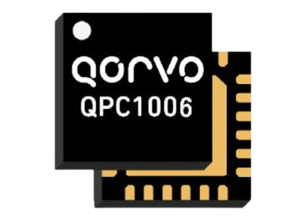
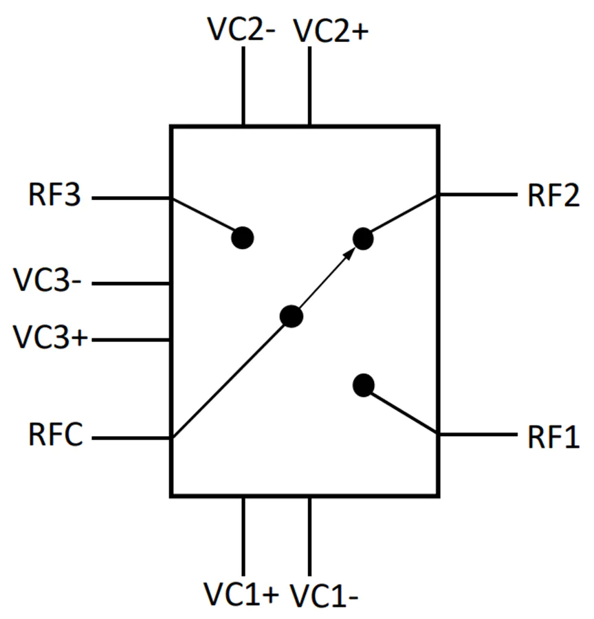
Qorvo QPC1006 Single-Pole, Triple–Throw (SP3T) Switch is fabricated on Qorvo’s QGaN25 0.25um GaN on SiC production process. Operating from 0.15 to 2.8GHz, the QPC1006 typically supports 50W input power handling at control voltages of 0/−40V for CW and pulsed RF operations. This switch maintains a low insertion loss of less than 1.0dB and greater than 30dB isolation, making it ideal for high-power switching applications across defense and commercial platforms. The Qorvo QPC1006 is offered in a 4mm x 4mm plastic overmolded QFN package.
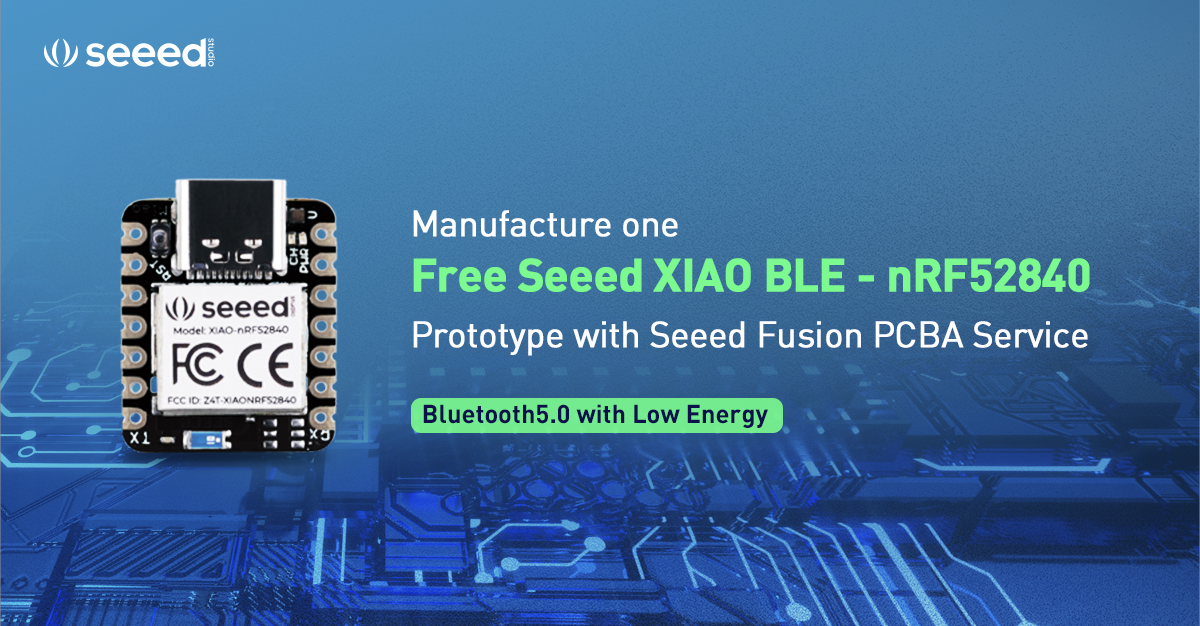
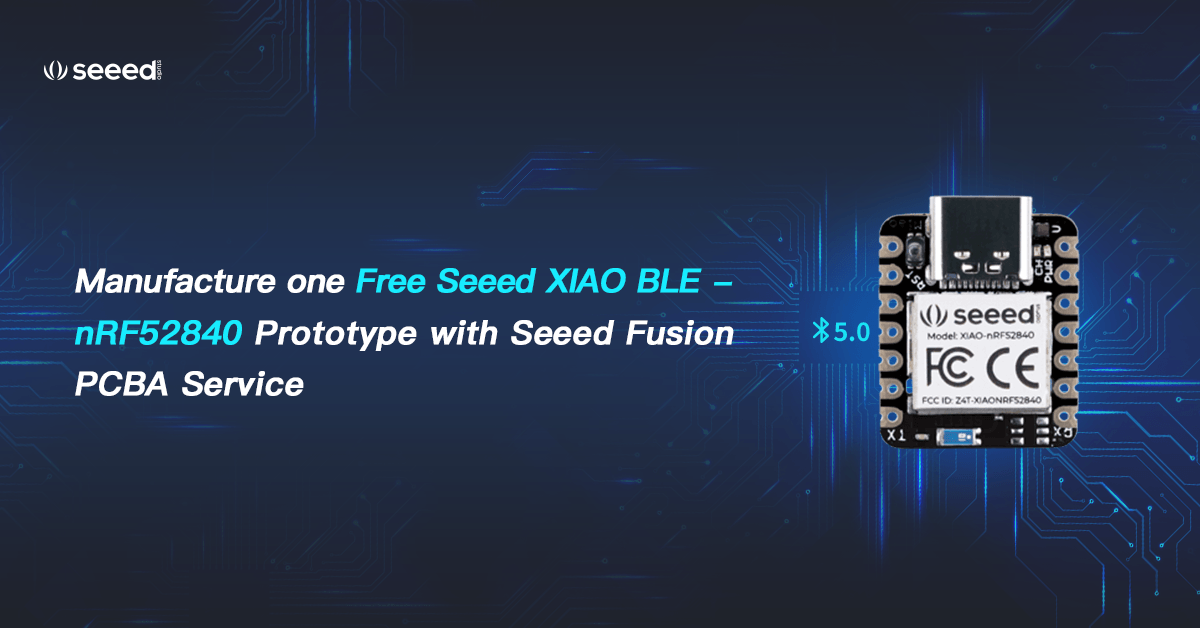
Seeed Studio has just released the highly anticipated addition to the XIAO series, Seeed XIAO BLE – nRF52840, a powerful Bluetooth LE microcontroller supporting multiple protocols including Bluetooth 5.0, NFC and Zigbee.
What’s so special about it? Seeed XIAO BLE and the advanced version, Seeed XIAO BLE Sense are designed for wearable devices and Internet of Things projects, taking advantage of the Nordic nRF52840 MCU’s Bluetooth capabilities of working at long distances, at low power yet with high performance.
The onboard antenna, small size and surface-mountable design make it highly suitable for connected, wearable designs, Internet of Things projects and the possibilities to run AI using TinyML and TensorFlow™ Lite.
Get inspired! To better support Internet of Things developers and enthusiasts to utilize this tiny yet feature-rich board, and accelerate the implementation of IoT industry, smart wear projects and TinyML, Seeed has launched a sponsorship event, manufacture your Seeed XIAO BLE prototype for free with Seeed Fusion PCBA service.
What is Seeed XIAO BLE?
Seeed XIAO BLE – nRF52840 is a low-power, ultra-small size, super cost-effective Bluetooth development board based on the powerful Bluetooth 5.0 MCU — Nordic nRF52840.
What are the key features of Seeed XIAO BLE?
One look at Seeed XIAO BLE and it’s hard to imagine that this cute board is a powerful wireless development board. Sharing the same form-factor with another Seeed favorite, Seeed XIAO BLE uses the thumb-size, surface-mountable design as other boards in the XIAO family. But on this tiny board is the powerful Bluetooth ARM Cortex®-M4 MCU, Nordic nRF52840 with Bluetooth 5.0 BLE, NFC and Zigbee support, an onboard antenna, battery management chip and 2MB high-speed QSPI flash for MicroPython and CircuitPython programming.
In addition to its small size and battery management, the ultra-low power consumption with a deep sleep current of less than 5μA makes it ideal for battery-powered IoT applications, wearables and small projects. And with the onboard QSPI flash, Seeed XIAO BLE is fully compatible with Arduino IDE & MicroPython/CircuitPython programming languages, and the large comprehensive libraries make it easy to get started with IoT projects.
With new wireless capabilities and as the smallest and most versatile nRF52840 development board available, Seeed XIAO BLE is set to be a gamechanger in the IoT and wearables space.
Get one piece of your Prototype Seeed XIAO BLE design manufactured for free with Seeed Fusion PCBA Service
When the original Seeeduino XIAO was launched, many engineers and makers alike were interested in using XIAO, and we received a lot of positive feedback from our customers in forums and on social media platforms.
Therefore, in order to stimulate enthusiasm and help commercial customers land more productive and valuable landing projects. Seeed are sponsoring Seeed XIAO BLE -nRF52840 designs with the Seeed Fusion PCBA service.
How to apply:
All you need to do is fill in the form and complete your Seeed XIAO BLE design.
Then add your order to the cart and we will confirm the application and get back to you with a coupon for one free PCBA piece. If you are looking for a powerful Bluetooth LE microcontroller for your next design, don’t miss this opportunity. Committed to providing one-stop electronic hardware services for over a decade, Seeed Fusion has the expertise and engineering insight to deliver streamlined PCB assembly at low costs and is equipped with a wide range of value-added services and capabilities.
Take advantage of the FreeDesign for Assembly review and Free functional testing with Seeed Fusion PCBA service now. Business users will also be interested in Seeed’s free prototyping sponsorship for business users. When your product reaches the batch production stage, we will deduct all the prototyping costs for that design up to 6% of the batch production value. If you are very interested in our product, but do not want to draw schematic and lay out by yourself for some reason, you are welcome to experience our ODM service. For more information, please contact fusion@seeed.cc for help.
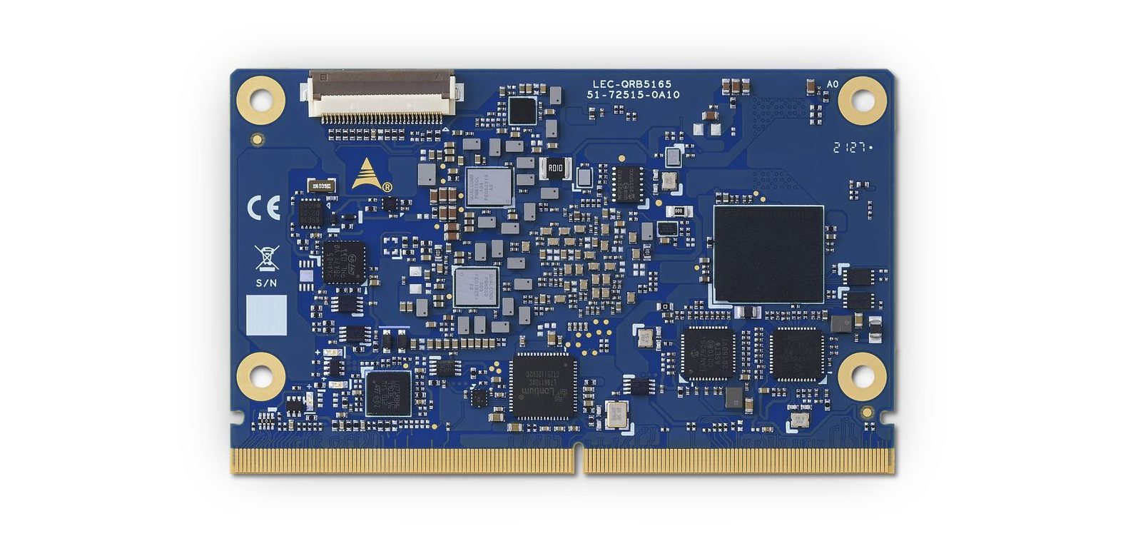
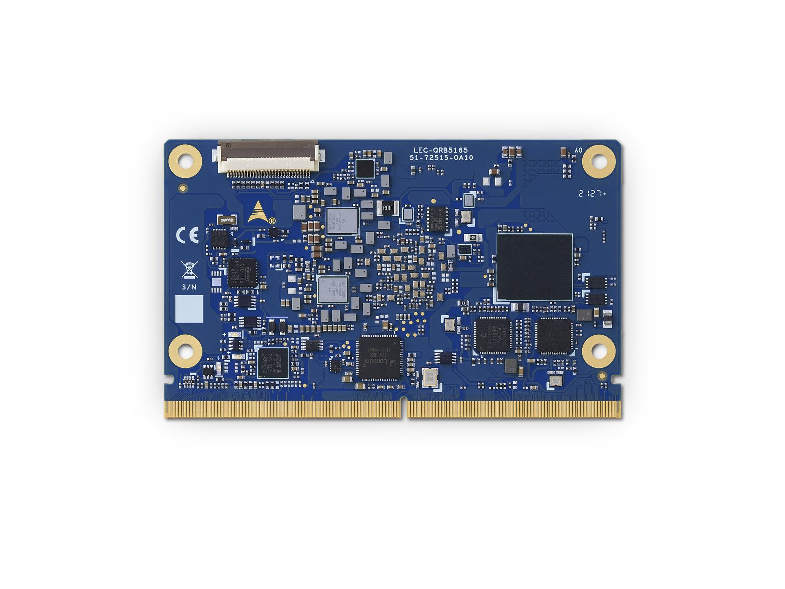
ADLINK releases its first SMARC module based on Qualcomm QRB5165 enabling high-performance robots and drones at low power Integrated IoT technologies provide on-device AI capabilities at the edge.
ADLINK Technology Inc., a global leader in edge computing, released the LEC-RB5 SMARC module –its first SMARC AI-on-Module based on a Qualcomm Technologies, Inc. processor. The Qualcomm QRB5165 processor is designed for robotics and drones applications and integrates several IoT technologies in a single solution. The LEC-RB5 SMARC module provides on-device artificial intelligence (AI) capabilities, support for up to 6 cameras, and low power consumption. It is capable of powering robots and drones in consumer, enterprise, defense, industrial and logistics sectors.
“This high performing SMARC module is a good option for the next generation of high-compute, low power robots and drones,” said Henri Parmentier, Senior Product Manager, ADLINK. “It empowers customers to do everything they need for complex AI and deep learning workloads at the edge without relying on the cloud.”
“Qualcomm Technologies’ portfolio of leading robotics and drones solutions is driving next-generation use cases including autonomous deliveries, mission critical use cases, commercial and enterprise drone applications and more. The Qualcomm QRB5165 solution supports the development of next generation high-compute, AI-enabled, low power robots and drones for the consumer, enterprise, defense, industrial and professional service sectors that can be connected by 5G. The ADLINK LEC-RB5 SMARC module will support the proliferation of 5G in robotics and intelligent systems,”
said Dev Singh, Senior Director, Business Development and General Manager of Robotics, Drones and Intelligent Machines, Qualcomm Technologies, Inc.
For robotics and autonomous robot solution providers, the LEC-RB5 SMARC module provides the capability to build powerful robots for use in harsh industrial conditions and in temperatures that range from -30° to +85°C. The LEC-RB5 SMARC module features:
Qualcomm® Kryo™ 585 CPU (8x Arm Cortex-A77 cores)
Qualcomm® Hexagon™ Tensor Accelerator (HTA) running up to 15 trillion operations per second (TOPS)
Six cameras support: MIPI CSI cameras CSI0 (2 lanes) and CSI1 (4 lanes)
Low power consumption: <12W
82 x 50 mm small size form factor
The LEC-RB5 is part of ADLINK’s portfolio of SMARC form factors that support both ARM and x86 designs. ADLINK has worked closely with Qualcomm to design a smart, powerful solution for next generation IoT applications. The module provides enhancements for computer vision (CV) applications with reduced latencies for real time image processing decisions, freeing up capacity for other critical AI applications while delivering mobile-optimized CV experiences. Hardware acceleration for advanced CV applications with on-device AI capable of running complex AI and deep learning workloads with low power makes the LEC-RB5 SMARC module advantageous for a wide variety of industrial and consumer applications.
Visit ADLINK Technology to learn more about the LEC-RB5 SMARC module and development kit.
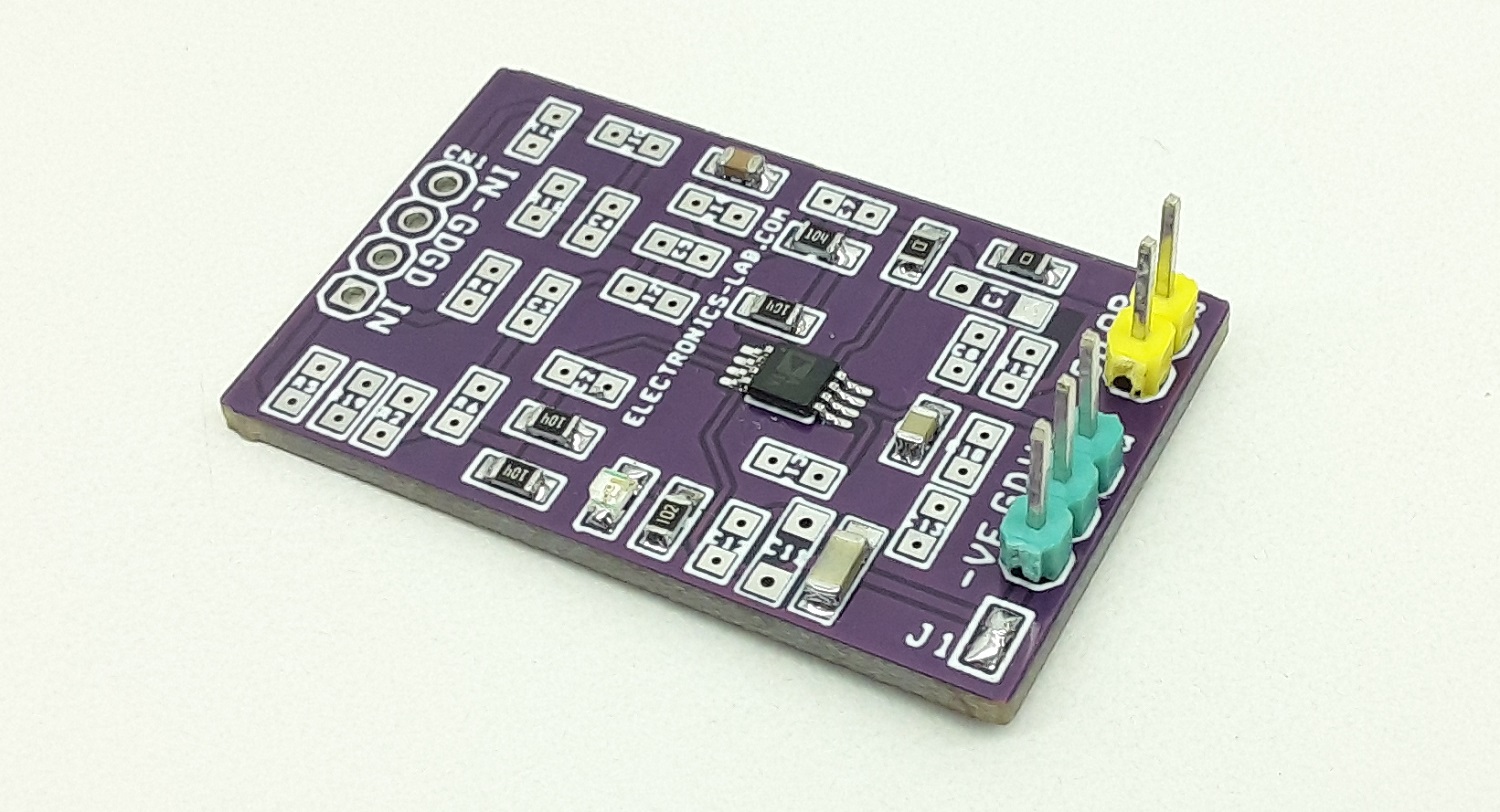
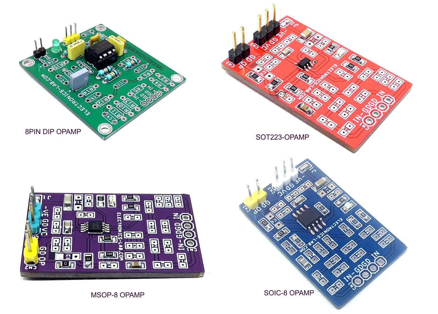
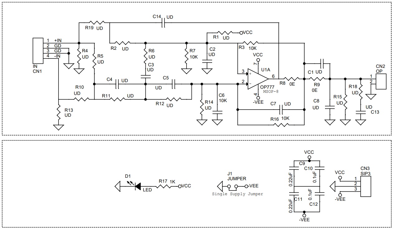
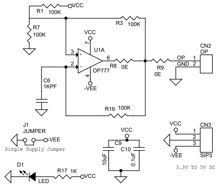
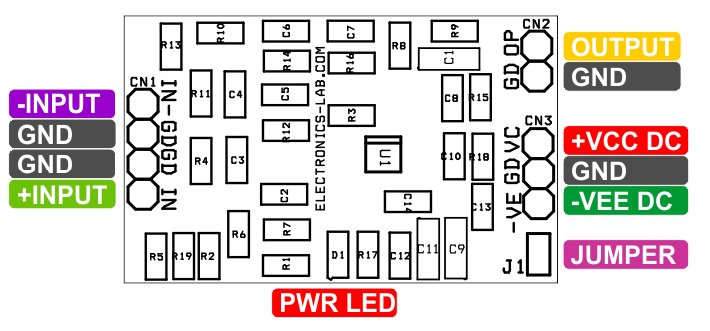
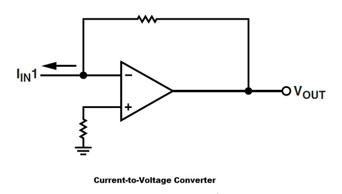
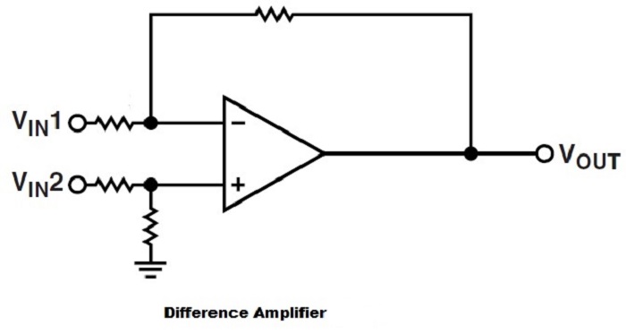
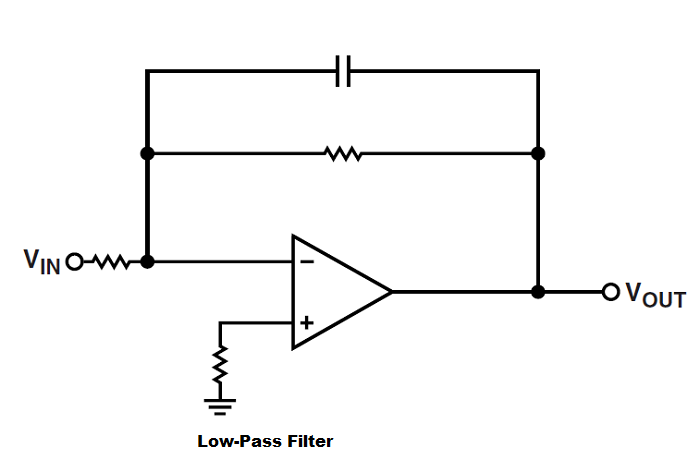
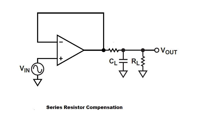
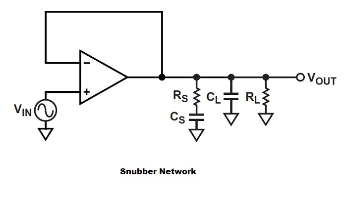
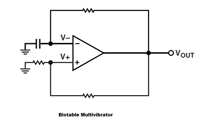
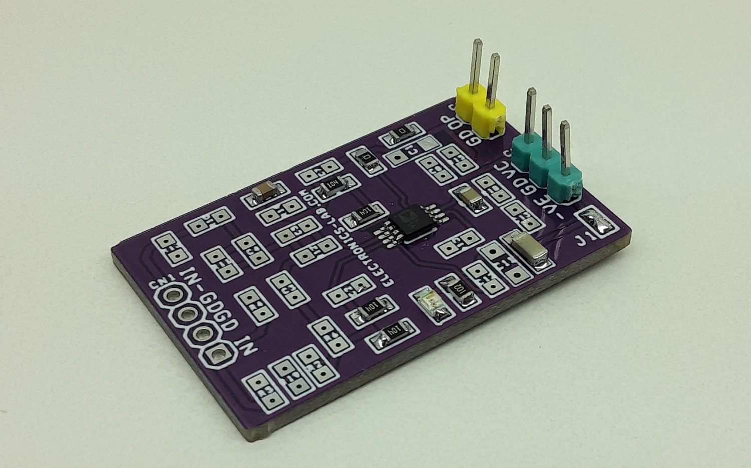
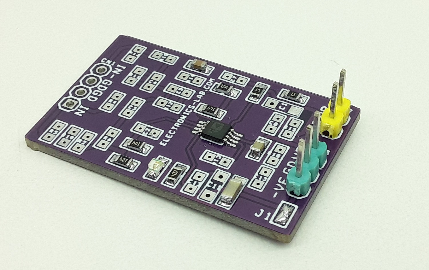
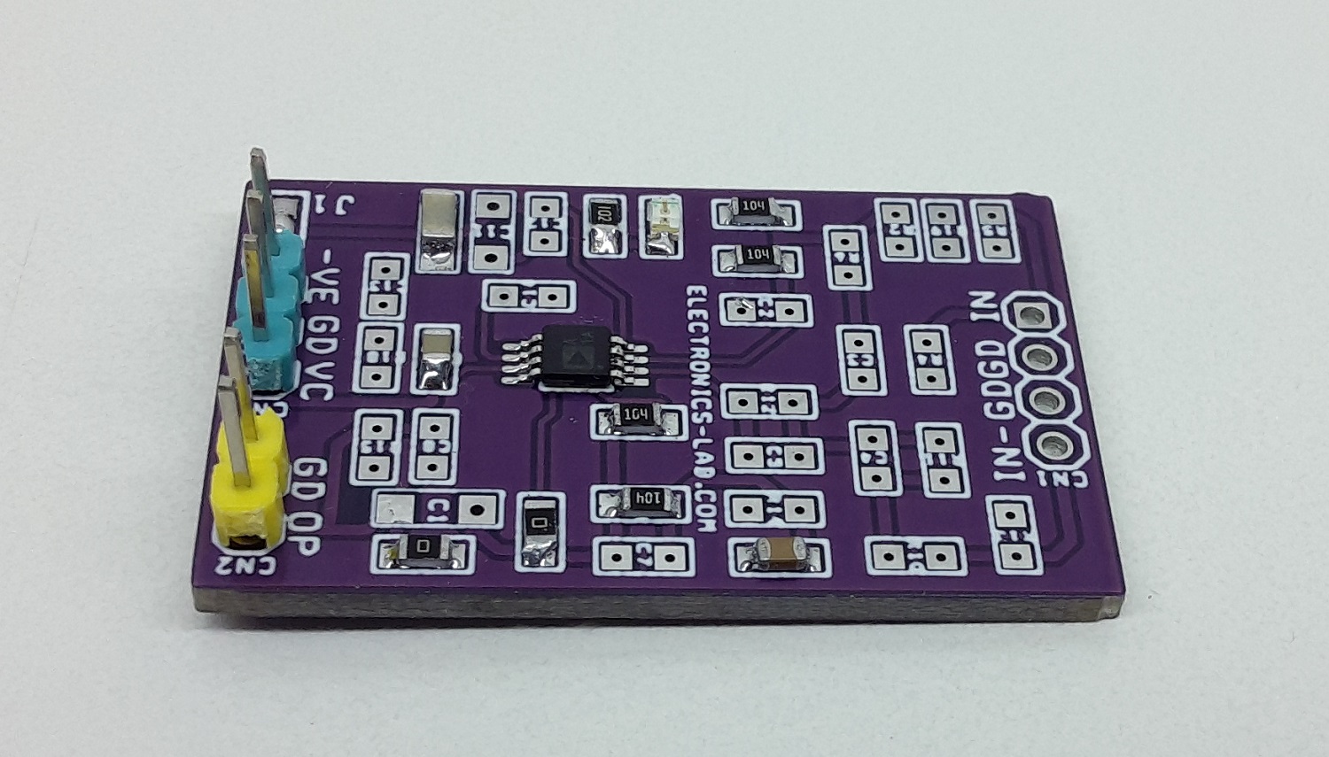
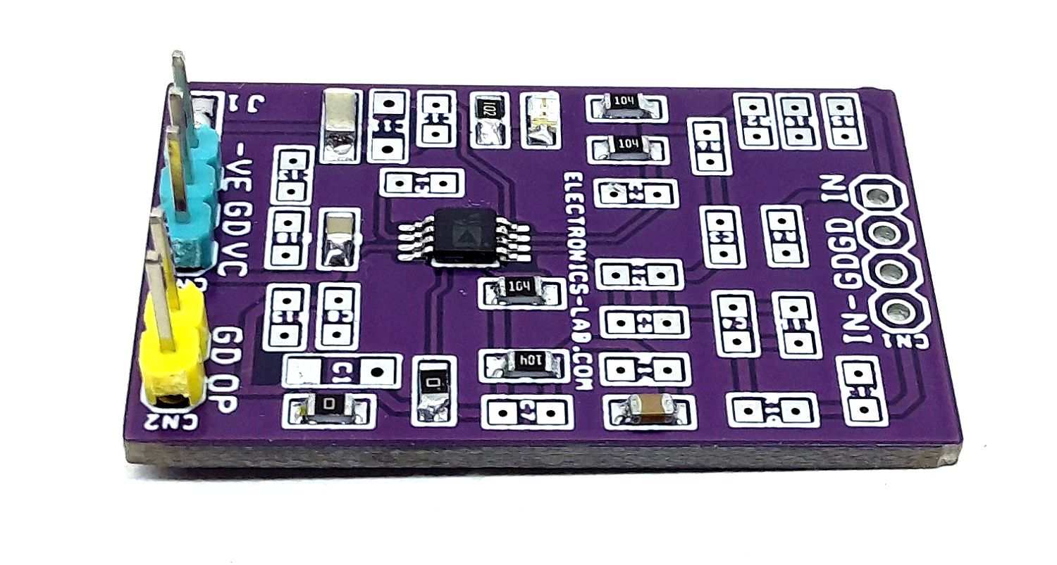
This is easy to build and very useful project for hobbyists and students to learn and create OPAMP-based projects. The project accommodates a single OPAMP in the MSOP8 package. The project provides the user with multiple choices and extensive flexibility for different applications circuits and configurations. It provides the user with many combinations for various circuit types including active filters, differential amplifiers, and external frequency compensation circuits. A few examples of application circuits are given below. OP777 op-amp is the right choice to use or any other MSOP8 op-amp with the same pin configuration as OP777 can be used. It supports dual supply or single supply, Jumper J1 is provided to use this board with a single supply, D1 is the power LED.
Note: Refer to example circuit to test the board, it is a bistable multivibrator, with a single supply and Jumper J1 closed.
Credits: All example schematics are from Analog Devices application notes.
Features
Single or Dual Supply User-defined (Jumper)
4 Pin Male Header Connector for inputs
3 Pin Male Header for Supply input (Single or Dual)
Jumper J1 Close for single Supply, Open for Dual Supply
LED D1 Power LED
Any MSOP8 Op-Amp Can be used (Pin configuration compatible OP777)
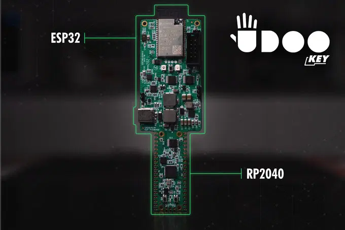
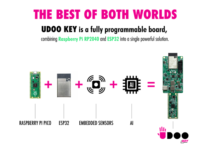
A number of AI boards have reached the hardware market for DIY and makers in the past years but none seem to be as flexible as the UDOO KEY. The UDOO KEY is an UDOO-Italy newest launch created with both Raspberry Pi RP2040 and ESP32 on a single board for flexible AI solutions.
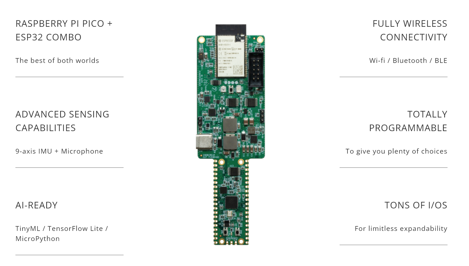
The board is fully programmable to give flexibility of choices, allowing the use of either RP2040, ESP32, or both at the same time for applications. The RP2040 based aspect of the board features dual ARM Cortex-M0 with 64 M-bit external QSPI flash, 246KB SRAM and 133MHz speed while the ESP32 compatible compatible part carries a dual-core Xtensa 32-bit LX6 with 16MB flash, 8MB PSRAM, WiFi, Bluetooth and Bluetooth Low Energy (BLE). The ESP32 module also supports full access to ESP32 firmware for programming on your terms.
The UDOO KEY is built to grant user access to UDOO’s AI platform, Clea, and pre-trained AI models for quick solutions in DIY, IoT analytics, over-the-air updates and AI applications. The UDOO KEY supports an accessory compatible with Raspberry Pi Pico and Olimex UEXT modules – ESP32 support. The board is also equipped with a 9-axis IMU and a microphone for high-end sensing functionalities as well as several inputs and output interfaces for large expandability.
The UDOO KEY also supports serial communication via a serial port and can be programmed through a USB-C port. The UDOO KEY is promoted as an open-source and open-hardware device and UDOO promises to release its BOM and Schematics as soon as shipping begins.
Key Features and Specifications Include:
ESP32-WROVER MCU — 8MB PSRAM, 16MB flash
RP2040 MCU — 246KB SRAM, 64M-bit QSPI flash
Wi-Fi, Bluetooth and BLE
9-AXIS IMU motion sensor and Omnidirectional digital microphone
5V DC via USB-C
ESP32-WROVER-E — UEXT connector (I2C, SPI, UART)
RP2040 — 26 GPIO pins (with 3 analog inputs), 2 x UART, 2 x SPI controllers, 2 x I2C controllers, 16 x PWM channels, 8 programmable I/O
Dimension: 130 mm x 40 mm
As for the software, both the pico and ESP32 MCU support TinyML, TensorFlow Lite, MicroPython,C/C++ programming environment, Arduino IDE, and a fully open-source free RTOS firmware. It also supports some common and ready-to-use SDKs and Clea. Clea is an AI and IoT platform based on Astarte and Edgehog open-source projects. While Astarte allows management and processing of IoT data with ESP32 SDK of ESP-IDF, Edgehog allows fleet management and over-the-air updates.
The UDOO KEY supports applications like predictive maintenance, sound recognition, keyword recognition, object detection, gesture recognition, and face recognition.
As of this writing, the campaign for UDOO KEY just ended on Kickstarter under 12 rewards between $4 and $382 with estimated delivery in January 2022 (worldwide). Its sales are expected to commence soon, but you can keep in touch with UDOO by signing up with your email to know when the UDOO KEY is available.
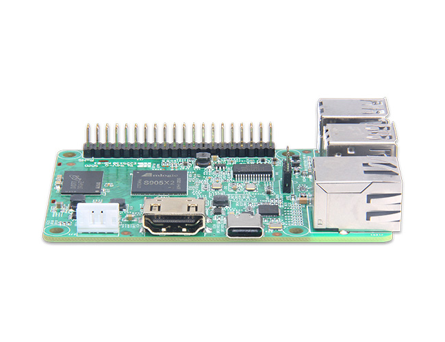
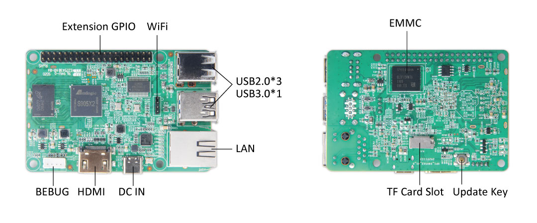
Geniatech, a leading OEM/ODM company specialized in providing open android based hardware and software platforms has returned with an android-supported XPI-S905X2/X3/X4 SBC built with a choice of three quad-core Amlogic SoCs: the Cortex-A53 based S905X2 and the Cortex-A55 based S905X3 and S905X4.
The Amlogic’s quad -A53 S905X2 SoC is an updated version of the S905X that was used in the XPI-S905X board while the 12nm fabricated, quad -A55 Amlogic S905X3 is a modest -A55 based update of the S905X2 with the addition of an optional 1.2-TOPS NPU and Cortex-M MCUs. The S905X4 on the other hand appears to be almost identical to the S905X3, just that there is additional support for the new AV1 codec at up to 4K@120fps. The S905X4 is also primarily aimed at the Android set-top market, which is the company’s specialty.
Geniatech’s XPI-S905X2/X3/X4 SBC can be has described as a Raspberry Pi 3 lookalike with features like 2GB RAM, 8GB eMMC, GbE, HDMI, 4x USB, 40-pin GPIO, an optional WiFi/BT, and a 85 mm x 56mm footprint.
Key Features and Specifications of the XPI-S905X2/X3/X4 SBC include:
CPU: Amlogic S905X2 (4x Cortex-A53), or S905X3/S905X4 (4x Cortex-A55)
GPU: Mali-G31 @ up to 650MHz
2GB RAM (1GB optional)
8GB eMMC (16GB or 32GB optional)
MicroSD slot for up to 64GB
1x Gigabit Ethernet port
Optional dual-band 802.11b/g with Bluetooth 4.0
HDMI 2.0 port
USB 3.0 host port
3x USB 2.0 host ports
Micro-USB port for power input
Serial debug connector
40-pin GPIO header (28x GPIO with support for UART, I2C, SPI, PWM GPIO, etc.)
Update key and optional cooling pad
5V power supply via micro-USB; optional adapter
Dimensions: 85 mm x 56 mm
OS: Android 9.0 but there’s a possibility that it is compatible with Linux
The XPI-S905X2/X3/X4 SBC also referred to as the 4K Single Board ARM PC is designed for a number of applications in fields like education, industrial control, etc.
Compared with other open-spec boards that are almost similarly configured, like the Banana Pi BPI-M2 Pro and the slightly more feature-rich Odroid-C4, the XPI-S905X2/X3/X4 appears to be less expensive but proprietary and without much in public documentation.
The XPI-S905X2 and XPI-S905X3 are currently available and are sold for $35 and $42 respectively, while the XPI-S905X4 seems not to be available yet. The board comes with an optional wireless module that is also available and sold for an additional $5.
Other useful details on the SBCs as well as where to purchase them may be found on the product page.
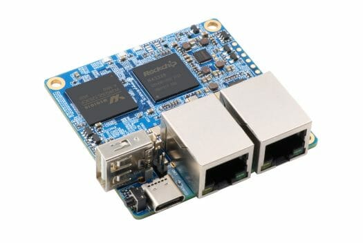
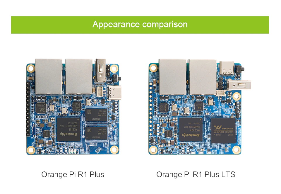
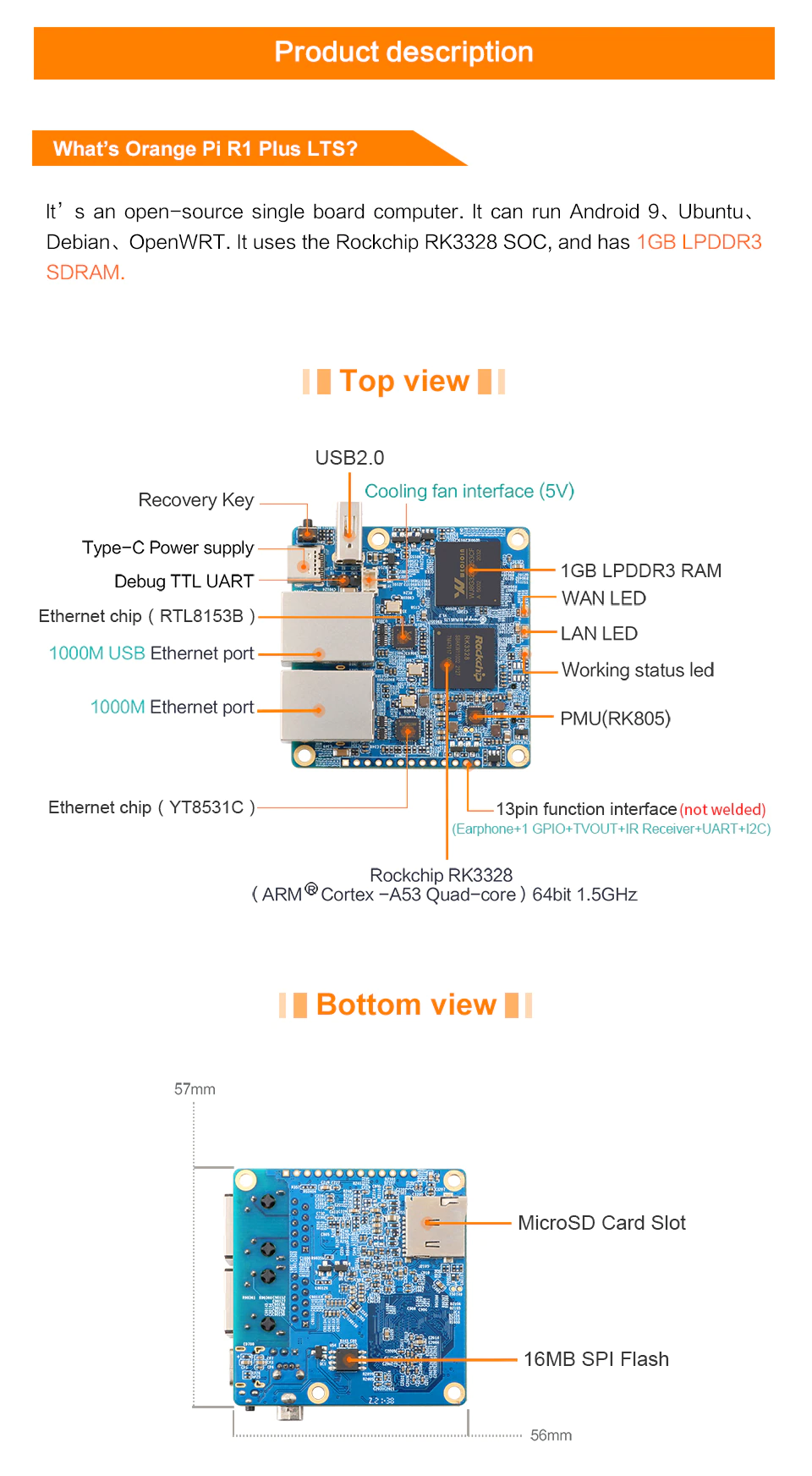
Just about a year ago, Shenzhen Xunlong Software updated its Orange Pi range of boards with an Orange Pi R1 Plus SBC powered by a Rockchip RK3328 quad-core Cortex-A53 processor running @ 1.5 GHz, coupled with 1GB RAM, dual Gigabit Ethernet ports, and one USB port for router applications. Now, the company has added to this line of the board a new Orange Pi R1 Plus LTS, which is exactly like Orange Pi R1 Plus SBC except that it replaced the Realtek RTL8211E PHY with a YT8531C Ethernet PHY and comes at a lower price.
Since the new Orange Pi R1 Plus LTS is quite similar to the older version, it means it can still be used for headless operations. Use cases include building a soft router, a computer, a wireless server, a speaker, and many more because it is open-source.
The new SBC is also powered by a Rockchip RK3328 processor, coupled with 1GB RAM, 2x GbE, and a single USB 2.0 port. The two boards are said to be with the same performance configuration.
Other Features and Specifications of the Orange Pi R1 Plus LTS SBC include:
Rockchip RK3328 quad-core Cortex-A53 @ 1.5 GHz with Arm Mali-450MP2
1GB LPDDR3 RAM
MicroSD card slot
16 MB SPI flash
2x Gigabit Ethernet via YT8531C Ethernet PHY and RTL8153B USB 3.0 to Ethernet chip
1x USB 2.0 port
1x USB-C OTG port
Unpopulated 13-pin header with earphone, 1x GPIO, TV out, UART, I2C, and IR receiver signals
3-pin header for serial console, fan header
Recovery key
WAN & LAN LEDs on board
Status LED.
Power Supply: 5V/2A via USB-C port or 2-pin header; RK805 PMU
Dimensions: 57 mm x 56 mm
Weight: 29.5 g
Supported Operating System: Android 9, Ubuntu, Debian, and OpenWrt
Apart from the difference in Ethernet PHY and the difference in system memory (LPDDR3 RAM instead of DDR4), and of course the fact that the YT8531C Ethernet transceiver would require a different driver, the company also mentioned that the firmware images are different.
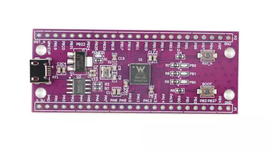
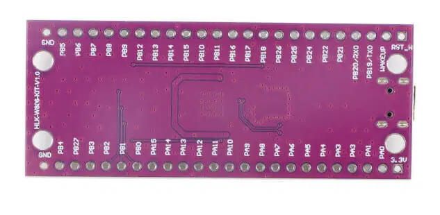
Shenzhen Hilink Electronics has released an inexpensive development board that utilizes the powers of the W806 MCU, a controllable IoT chip that offers high integration, low-power consumption, and low cost. The HLK-W806 development board which just hit the hardware market is based on the WinnerMicro W806 32-bit XT804 processor with 240MHz, inbuilt 1MB flash, and 288KB RAM. The board is equipped with an RST reset button, USB2.0 port, touch, UART, PWM, GPIO, SPI, I2S, ADC, and LCD interfaces. It is targeted to help IoT solution developers to evaluate W806 chips, realize more functions and build prototypes faster. The W806-based board is only debugged via the Ck-Link emulator since its MCU features Pingtou’s CDK development environment. Although not showing features of wired or wireless communication means, Hilink still promotes HLK-W806 as IoT MC.
As for the W806 MCU, Reddit says it is a RISC-V MCU using T-Head’s XuanTie E804 IP, but a user argues that XuanTie E804 is C-SKY ISA and not RISC-V. Another user also confirms that the MCU is not RISC-V and with that, it will likely be a C-SKY ISA. The reason is that C-SKY is mentioned in RISCV as a member of the RISC-V foundation with CPU architecture for low-power SoCs. And that the company does plumb C-SKY support into Linux/open-sources protocols and other toolchains.
Key Features and Specifications of HLK-W806 and W806 MCU:
1x SDIO_ HOST interface, support SDIO2.0, SDHC, MMC4.2
1 x SDIO_ DEVICE, support SDIO2.0 @ 200Mbps
1 x I2C controller
GPIO controller @ 44 GPIO
5-channel PWM interface
1 channel Duplex I2S controller
LCD controller @ 4×32 interface
Documents on W806 MCU chip specification (although not in English), application manual (.zip), hardware information (.zip), SDK (.rar), and W800 serial burning tool (.rar) can be found on HLK-W806 details.
For ordering and shipping, the HLK-W806 is available for purchase for under $2.00 on AliExpress.
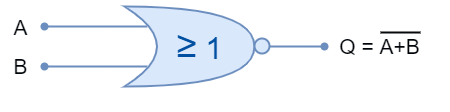
The logic NOR function gives the inverted output of the logic OR function. It complements the output of the logic OR function to give the NOT OR (NOR) function. The logic NOR function is the combination of two logic functions that are OR & NOT logics. These OR & NOT logics form a series combination to produce the logic NOR function.
Figure 1: The NOR gate equivalent
The combination of these two logics is symbolized by placing an “Inversion Bubble” at the output of an OR gate. The logic NOR symbol is shown in the following figure along with its Boolean expression. The Boolean expression of the NOR gate is represented by a sum of inputs with an overline (¯). The sum of inputs expresses OR logic and, whereas, the overline (¯) represents the NOT logic.
Figure 2: The NOR gate symbol with expression
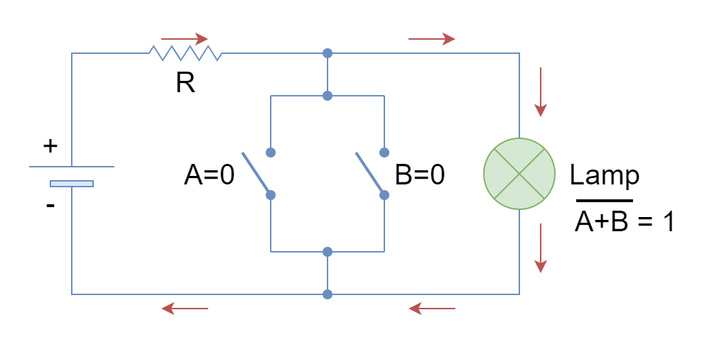
Similar to the logic OR function, the logic NOR function can be represented and explained by switches. From the previous article on Logic OR Function, it is known that OR function can be represented by parallel switches that are placed in series with the output. However, in the logic NOR function, these parallel switches (inputs) are placed parallel to the output. The representation of a logic NOR function in the form of switches is shown in the following figure.
The logical states of “0” & “1” represent a switch with “Open” & “Closed” positions, respectively.
Figure 3: The lamp ON when both switches are open
In the above figure, the current flows through the lamp to turn it ON when both switches (A & B) (inputs) are open (both at logic 0).
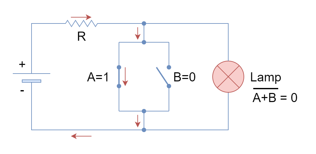
Figure 4: Lamp ON when any switch is closed
The closing of any of the switches changes the state of the lamp and turns OFF the lamp by providing an alternate low resistive path to a power source.
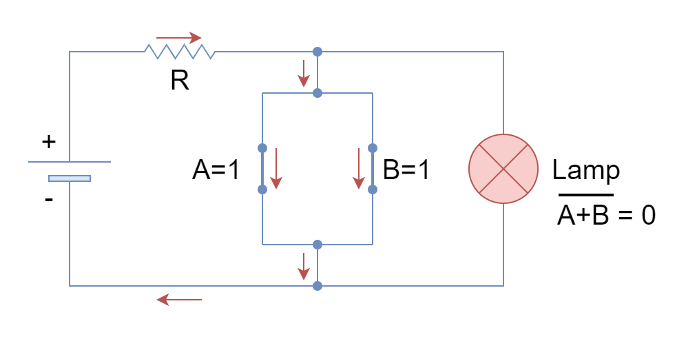
Figure 5: Lamp OFF when both switches are closed
The closing of both switches (both at logic 1) does not change the state of output and the lamp remains OFF until both of the switches are opened.
The only condition for the lamp to remain ON is when all of the switches are open or at a LOW state. This is in reverse with the logic OR function which, contrarily, turns ON the lamp when any of the inputs is at a HIGH state.
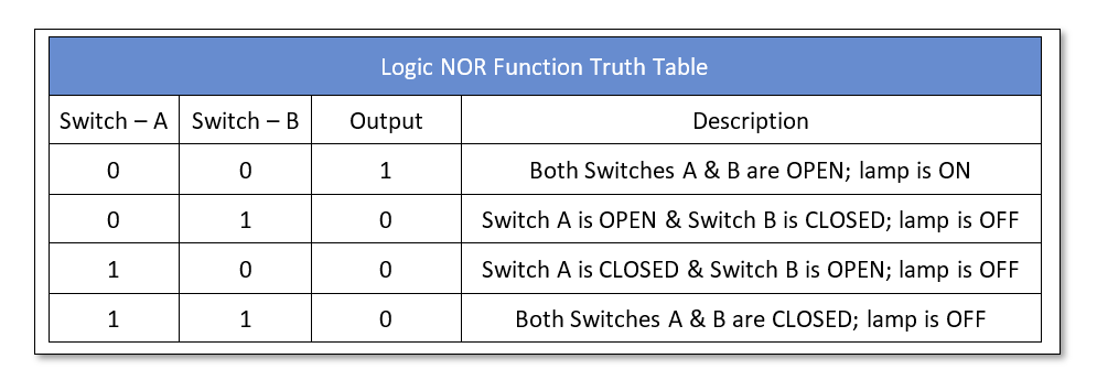
The switches representation of a logic NOR function is expressed in the form of a truth table which is given below:
Construction of NOR logic
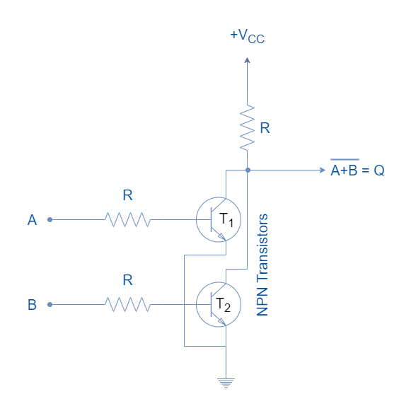
The logic NOR gate can be constructed using Resistor-Transistor Logic (RTL), Transistor-Transistor Logic (TTL), or Complementary Metal-Oxide Semiconductor (CMOS). These, basically, constitute the formation of logical families. The logic NOR gate with two inputs constructed using Resistor-Transistor Logic (RTL) is shown in the following figure.
Figure 6: The Resistor-Transistor Logic (RTL) NOR gate
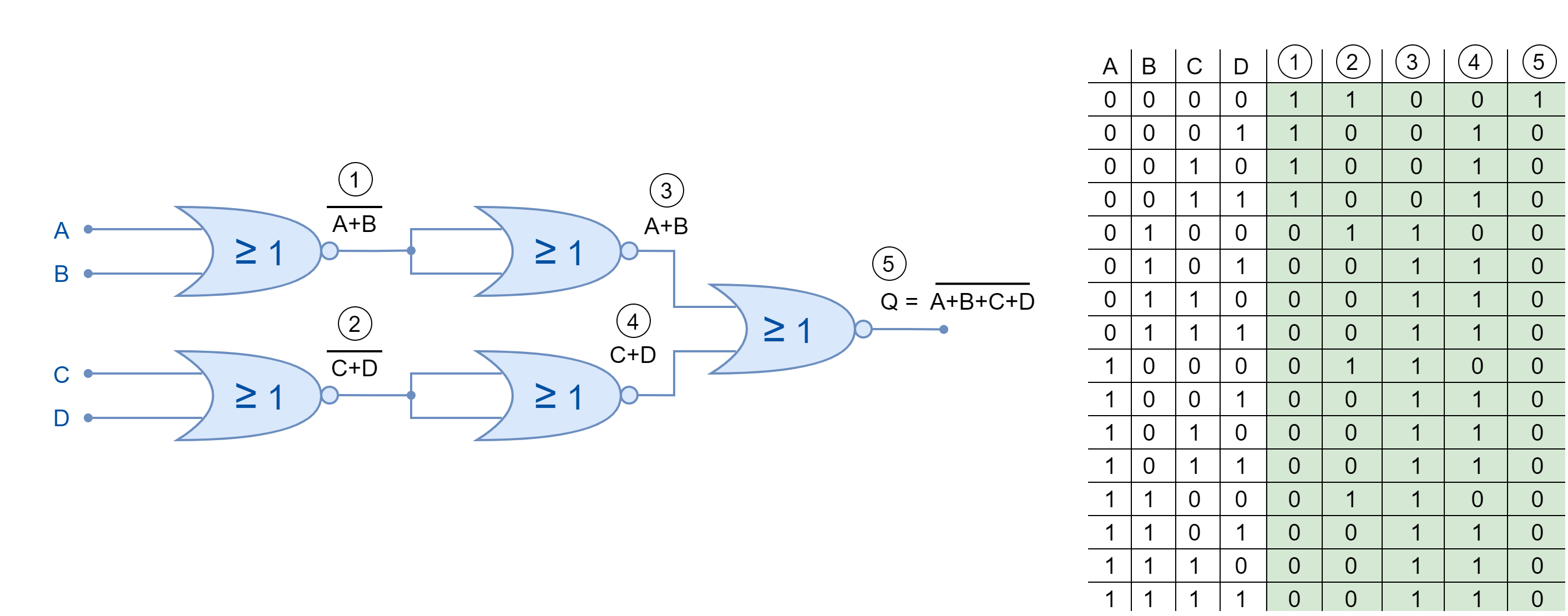
The logic NOR function can be extended to include more than two inputs. In Boolean expression form, the additional input or variable is added to the sum with an overline. In logic gates, the NOR gates are cascaded to add in more inputs as shown below.
Figure 7: The logic NOR gate with more than two inputs
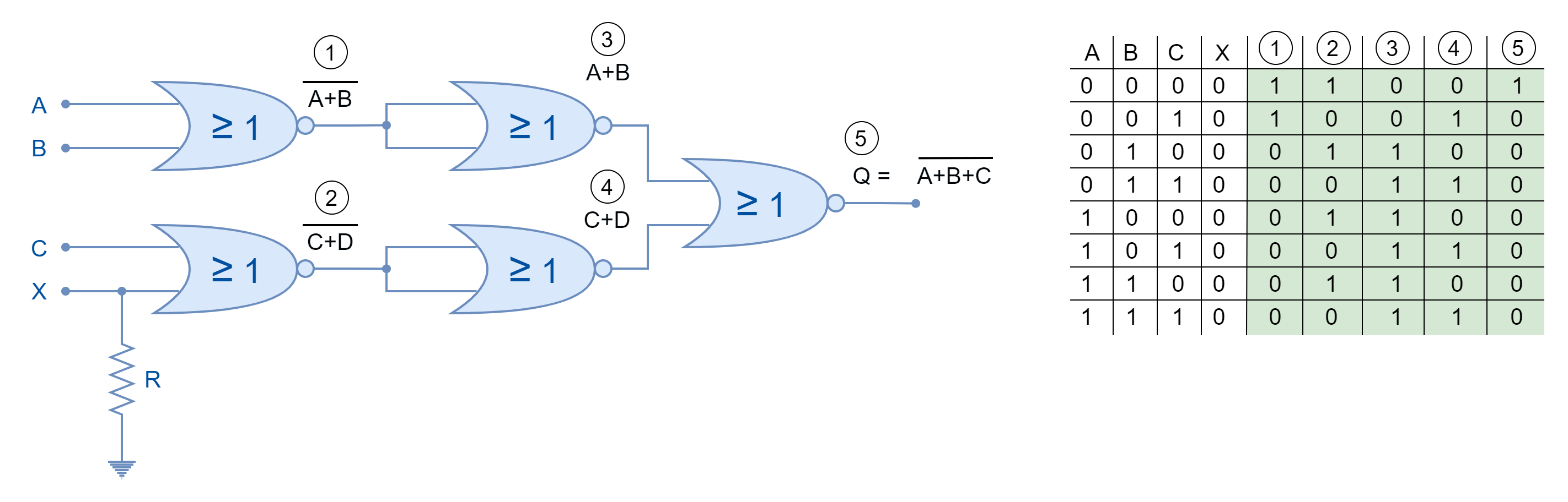
Moreover, the logic NOR function with an odd number of inputs can also be achieved by using logic “LOW” or “0” in Boolean expression form. Whereas, in the case of NOR gates, the other input (unused/ discarded) must be pulled down through a suitable resistor as shown in the following figure.
Figure 8: The logic NOR gate with an odd number of inputs
Universal Gate
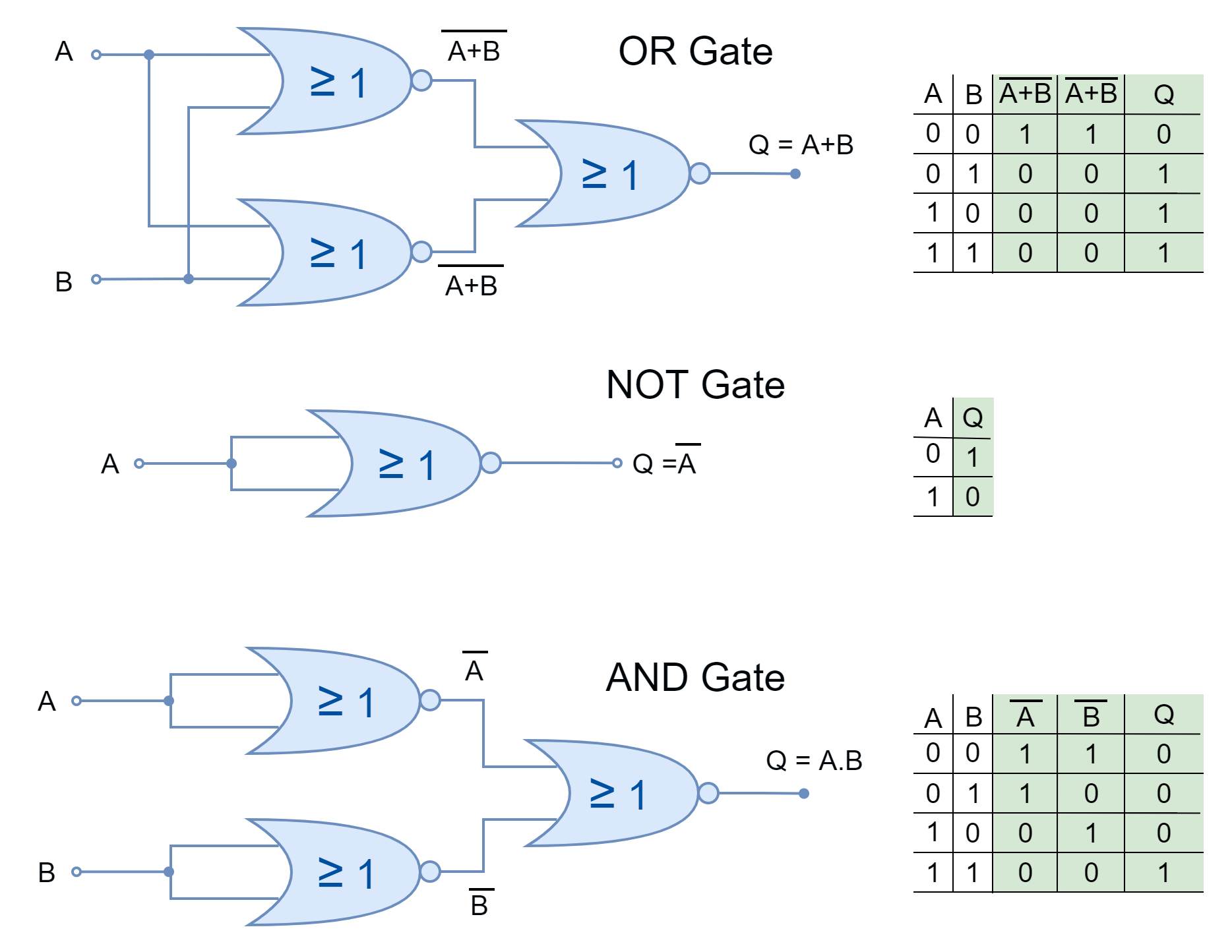
Just like the NAND gate, the logic NOR gate is also referred to as a Universal Gate as every other logic function can be constructed using it. They can construct all the functions which can be constructed using basic logic gates i.e. AND, OR, and NOT. The construction of basic logic functions using logic NOR gates is shown below.
Figure 9: Basic logic function using NOR gates
Boolean Algebra Laws
Similar to the logic OR function, the logic NOR function follows all the Boolean algebra laws and theorems such as Annulment, Identity, Idempotent, Complement, Commutative and Associative Laws which are explained briefly in the Logic OR function.
Commercially Available Logic NOR Gates
The logic NOR gates are available in form of I.C. packages which contain multiple NOR gates with multiple inputs to each gate. The selection depends merely on the application and the number of logic gates is required. They come in both Transistor-Transistor Logic (TTL) and Complementary Metal Oxide Semiconductor (CMOS) family packages. A few commercially available logic NOR gates are given below:
74LS32 Quad 2-input
CD4071 Quad 2-input
CD4075 Triple 3-input
CD4072 Dual 4-inputs
Conclusion
The logic NOR function gives output TRUE only when all of its inputs are in a FALSE state.
Any of the inputs in the TRUE state will lead the NOR function to the FALSE output.
The logic NOR function can be represented by an electrical circuit having two parallel switches with the load. When any of the switches are closed (input at TRUE state) then supply bypasses the load/ lamp and turns it OFF.
The logic NOR gate is also known as Universal Gate because it can construct every other logic.
The logic NOR gates can be cascaded together to obtain logic NOR having more than two inputs.
The commercially available packages come in different I.C. packages. Each IC package contains multiple NOR gates.
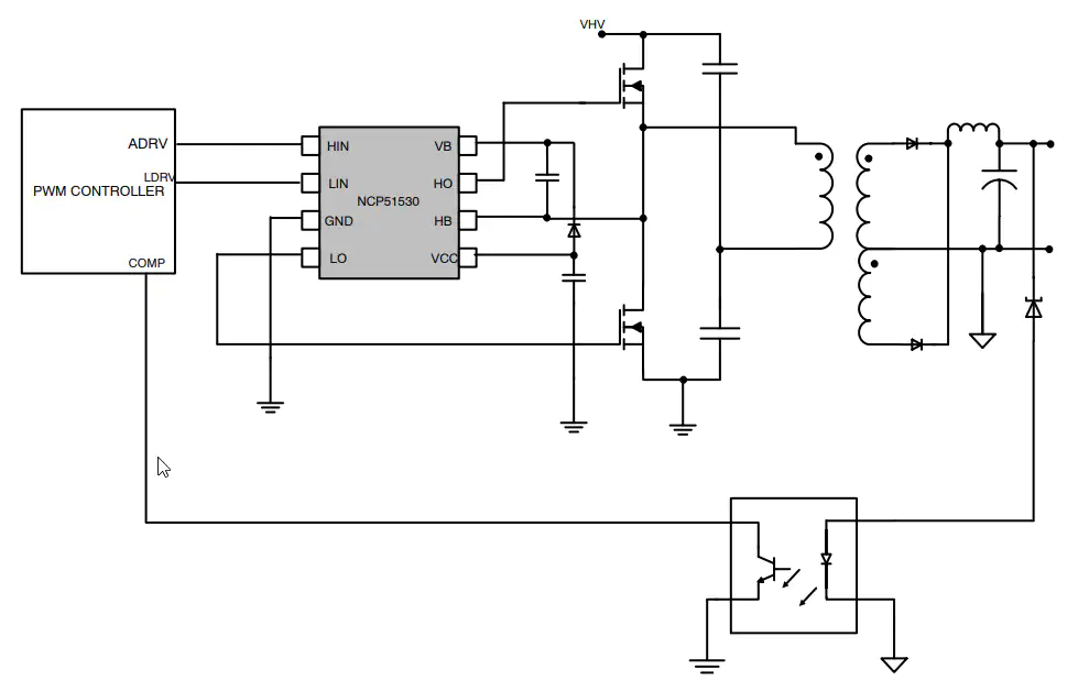
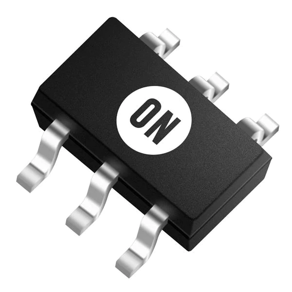
onsemi NCP51100A Low-Side Gate Driver is a 700V high side and low side driver with a 3.5A source and 3A sink current drive capability. The NCP51530 offers propagation delay, low quiescent current, and low switching current at high frequencies of operation. This device is tailored for highly efficient power supplies operating at high frequencies. The device is offered in two versions, NCP51530A or NCP51530B. NCP51530A has a typical 60ns propagation delay, while NCP51530B has a typical propagation delay of 25ns. NCP51530 comes in SOIC8 and DFN10 packages.
Features
High voltage range up to 700V
NCP51530A typical 60ns propagation delay
NCP51530B typical 25ns propagation delay
Low quiescent and operating currents
15ns max rise and fall time
3.5A source/3A sink currents
Under-voltage lockout for both channels
3.3V and 5V input logic compatible
High dv/dt immunity up to 50V/ns
Pin-to-Pin is compatible with industry-standard half-bridge ICs
Matched propagation delay (7ns max)
High negative transient immunity on bridge pin
DFN10 package offers both improved creepage and exposed pad