Xassette-Asterisk RISC-V 64 SBC Features Allwinner’s latest D1s SoC and Sells for Less Than $10

Open-source embedded system framework has made processor and SBC innovation more fun and easy, offering many configurable architecture implementations. The RISC-V ISA based hardware, though not very economical, is still very much celebrated even after more than a decade of its existence. So far, we have seen it in a number of devices including the Allwinner D1 based Nezha RISC-V Linux SBC currently sold for a little over $100, and the SdtElectronics’s Xassette-Asterisk, an evaluation board based on Allwinner’s latest D1s SoC coming out for under $10.

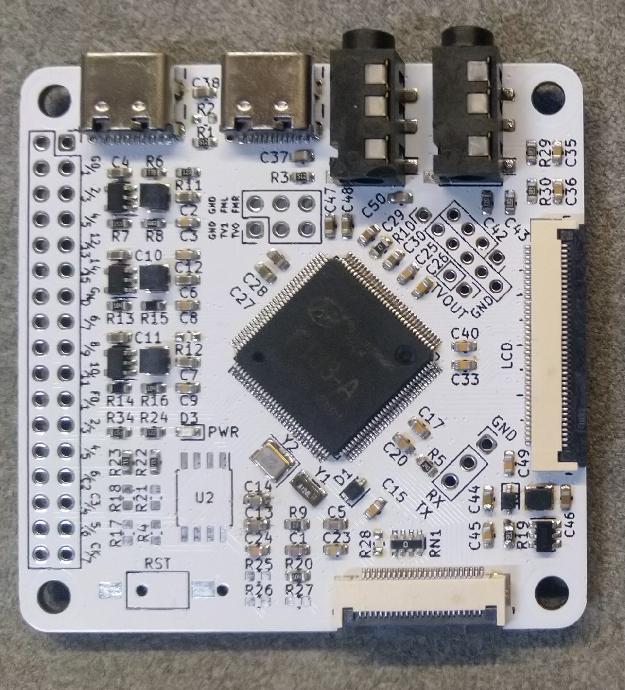
Xassette-Asterisk SBC features Allwinner’s single-core RISC-V 64 SoC, F133/D1s, which runs at 1.008GHz with an inbuilt 64MB DDR2, and an operating input voltage of 5V supplied via a USB-C port or 3.3V via pin header. The SBC also features digital and analog interfaces including USB ports, micro-SD slot, LCD connector, and headphone interface in a compact 56×56 mm – 2 layer board. According to SdtElectronics, the SBC has been tested with an 800×480 parallel LCD even though the F133 manual reveals support for up to 1920×1080 parallel LCD. The board, however, does not feature GMAC and WiFi modules, which the designer claims are to reduce complexity and cost, but it still supports easy internet access. SdtElectronics also claims that networks can be shared with a computer via RNDIS Gadget, a USB Ethernet support protocol of Linux-Sunix.

Key Features and Specifications of the board:

  • 1.008 GHz, 64MB DDR2, Allwinner D1s single-core 64-bit RISC-V chip
  • MicroSD card slot, 32 MBit SPI flash
  • 40-pin LCD interface, 6-pin touch panel interface, backlight power
  • 24-pin MIPI CSI interface
  • Headphone with mic jack (3.5mm), Line-in jack (3.5mm)
  • 1x USB Type-C OTG port
  • 1x USB Type-C host port (1)
  • 34-pin GPIO header with SPI, I2C, UART, PWM, DAC, ADC, IR Tx, R, power (5V, 3.3V, and GND)
  • 3-pin UART header (serial console usable)
  • Reset button
  • Power Supply:
    • 5V via USB-C port
    • 3.3V via pin header (Not supported by USB due to absence of 5V)
  • Dimension: 56mm x 56mm

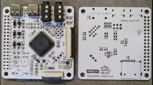
The Xassette-Asterisk is an open-source hardware product based on the Linux OpenWrt framework. The project’s log added a few days ago claims that D1s only boots the Tina Linux with limited functionality. So, the root directory of the Linux system had been modified to run the Ubuntu filesystem. SdtElectronics also claims that the package manager alongside Internet access supports high software packages. Documentary on PCB and schematics is available on the Github repository.

The Xassette-Asterisk is not for commercial purposes, but its progress is logged at Hackaday In case you want to join the project and build your board. You might have to purchase the Allwinner processor from Taobao for about $5.5 too.

Seeed’s $799 Jetson SUB Mini PC Kit Combines Leetop’s A206 carrier board with a Xavier NX Module

Seeed Studio has launched a Jetson SUB Mini PC Kit designed for AI applications. The 130 mm x 120 mm x 50mm combines Xavier NX module with an A206 carrier board from Leetop.

The Jetson Xavier NX module delivers up to 21 TOPS and with 384 NVIDIA CUDA cores, 48 Tensor cores, Hexa-core Carmel 64-bit ARM CPUs, and two NVIDIA deep learning accelerators engines. The module is also said also offer 8GB LPDDR4x and 8-32GB eMMC 5.1, and preloaded with Nvidia’s Ubuntu-powered Jetpack SDK for tapping it’s AI capabilities.

The Leetop A206 carrier board on the other hand has a number of features including dual MIPI-CSI camera interfaces, a CANBus header, and 40-pin GPIO. The module also has a real-time clock with coin cell socket, a 15V/3A DC input, and a -25 to 80° operating temperature range.

The Jetson SUB mini PC also comes with a case, a heat sink, and a fan. There’s also a 512GB SSD, WiFi and BT, GbE, HDMI, DP, and 4x USB. The kit is ideal for high-performance compute and AI in embedded and edge systems. It is a choice platform for running modern neural networks in parallel and process high-resolution data from multiple sensors simultaneously.

Features and Specifications of the Jetson SUB mini PC include:

  • NVIDIA Jetson Xavier NX module with:
    • 6-core NVIDIA Carmel ARMv8.2 64-bit processor with 6 MB L2 + 4 MB L3 cache
    • NVIDIA Volta architecture with 384 NVIDIA CUDA cores and 48 Tensor cores
    • 2x NVDLA Engines, 7-Way VLIW Vision Processor
    • Multiple 4Kp60 encode, multiple 8Kp30/4Kp30 decode
    • 8 GB 128-bit LPDDR4x 51.2GB/s
    • 10 W | 15 W | 20 W
    • Up to 14 TOPS @ 10 W, Up to 21 TOPS @ 20W
  • 1x MicroSD slot
  • M.2 Key M socket fitted with a 128GB NVMe SSD
  • HDMI and DisplayPort
  • 2x MIPI CSI-2 D-PHY lanes compatible with Raspberry Pi HQ camera and RPi V2 camera
  • Gigabit Ethernet
  • WiFi & Bluetooth via M.2 Key-E card (included)
  • 4x USB 3.1 ports
  • USB 2.0 Micro-B
  • Header with GPIOs, I2C, I2S, SPI, UART
  • Power supply: 9 to 19V DC via power barrel jack
  • Dimensions: 130 mm x 120 mm x 50 mm

The mini PC kit comes with everything needed in terms of hardware and software already installed and set up. It is available for order at $799. Shipping already started on the 5th November this year. You will get it with an acrylic cover, an aluminum frame and two external antennas.

Other useful details on the Jetson SUB Mini PC Kit may be found on Seeed’s Jetson SUB and the A206 carrier board product pages.

STEVAL-L6986IV1 Synchronous Iso-Buck Converter Evaluation Board

STMicroelectronics’ evaluation board with dual isolated output is based on the L6986I

STMicroelectronics’ 38 V, 5 W synchronous iso-buck converter evaluation board generates two isolated voltages (approx. +18 V and between -4 V and -5 V), suitable for supplying IGBT/SiC MOSFET gate drivers or a single isolated voltage using a simple bypass. The board features the L6986I switching converter allowing a fine and adjustable primary output voltage and an isolated secondary output generated using a transformer.

The primary sink capability (typ. 1.9 A) allows appropriate energy transfer to the secondary side and enables a tracked soft-start of the secondary output. The control loop is based on a peak current mode architecture with the device operating in forced PWM. The 300 ns blanking time filters oscillations generated by the transformer leakage inductance and renders the solution more robust.

Pulse-by-pulse current sensing on both power elements implements effective constant current protection on the primary side. At the same time, the secondary output is protected against short-circuit events because of the primary reverse current limit. The secondary voltage is stabilized over current with a power transistor and a shunt voltage reference (TL431).

Features

  • Designed for iso-buck topology
  • 4 V to 38 V operating input voltage
  • Primary output voltage regulation/no optocoupler required
  • 1.9 A typical sink peak primary current capability
  • Peak current mode architecture in forced PWM operation
  • 300 ns blanking time
  • 8 µA IQ-SHTDWN
  • Adjustable fSW and synchronization
  • Embedded primary output voltage supervisor
  • Adjustable soft-start time
  • Internal primary current limiting
  • Overvoltage protection
  • RDS(ON) HS = 180 mΩ, RDS(ON) LS = 150 mΩ
  • Thermal shutdown

more information: https://www.st.com/en/evaluation-tools/steval-l6986iv1.html

LTC3337 Primary Battery State of Health Monitor

Analog Devices Inc. LTC3337 Primary Battery State of Health (SOH) Monitor provides accurate, real-time readings of battery cell discharge, voltage, impedance, and temperature. The LTC3337 is designed to be placed in series with a primary battery with minimal associated series voltage drop. This device integrates an infinite dynamic range coulomb counter that tallies all accumulated battery discharge and stores it in an internal register accessible via an I2C interface. A discharge alarm threshold based on this state of charge (SOC) is programmable. When it is reached, an interrupt is generated at the IRQ pin. Coulomb counter accuracy is constant down to no load.

To accommodate a wide range of primary battery inputs, the peak input current limit of the LTC3337 is pin selectable from 5mA to 100mA.

Coulombs can be calculated for either the BAT_IN or BAT_OUT pin, determined by the AVCC pin connection. A BAL pin is provided for applications utilizing a stack of two supercapacitors (optional) at the output.

The Analog Devices Inc. LTC3337 Primary Battery State of Health Monitor is available in a 12-lead Lead Frame Chip Scale Package (LFCSP) with an exposed pad for improved thermal performance.

Features

  • 8.0V to 5.5V battery input voltage range
  • 100nA quiescent current
  • 8 primary battery peak input current limits
    • 5mA, 10mA, 15mA, 20mA, 25mA, 50mA, 75mA, 100mA
  • SOH monitor for primary battery
    • Integrated coulomb counter (Q)
    • Additional monitors for battery voltage (V), battery impedance (Z), and temperature (T)
  • Integrated ±10mA supercapacitor balancer
  • Primary battery current (BAT_IN) or load current (BAT_OUT) is counted
  • Programmable coulomb counter prescaler for a wide range of battery sizes
  • Programmable discharge alarm threshold with interrupt output
  • I2C interface
  • -40°C to +125°C operating junction temperature range
  • 2mm x 2mm LFCSP-12 package

Block Diagram

Application Circuit

more information: https://www.analog.com/en/products/ltc3337.html

Diodes Incorporated AP22816/17/18 Power Distribution Load Switches

Diodes Incorporated AP22816/17/18 1A/1.5A/2A Power Distribution Load Switches are single-channel, current-limited, integrated high-side power switches optimized for Universal Serial Bus (USB) and other hot-swap applications. The AP22816/17/18 are available with both polarities of enable input and comply with USB standards.

The Diodes Inc AP22816/17/18 Power Distribution Load Switches feature a 1A, 1.5A, or 2A output current, fast short-circuit response time, and an integrated output discharge function to ensure completely controlled discharging of the output voltage capacitor. The switches offer a complete protection solution with reverse current blocking, overcurrent, overtemperature, and short-circuit protection, as well as controlled rise time and undervoltage lockout functionality. The 6ms deglitch capability on the open-drain flag output prevents false overcurrent reporting and requires no external components.

The AP22816/17/18 Switches are available in the standard Green and RoHS compliant TSOT25 and MSOP-8 packages.

Features

  • Input voltage range of 2.7V to 5.5V
  • Logic level Enable pin available with active-high or active-low versions
  • Protections:
    • 2kV HBM, 500V CDM ESD Protection
    • Overcurrent protection with auto-recovery
    • Short-circuit protection with auto-recovery
    • Overtemperature protection with auto-recovery
    • Output reverse current / voltage protection
  • 75mΩ On-resistance
  • Built-in soft-start with 0.6ms typical rise time
  • Fault report (FLG) with blanking time (6ms Typ.)
  • Thermally efficient low profile package
  • Level 1 per J-STD-020 moisture sensitivity
  • Finish–matte tin-plated leads, solderable per MILSTD-202, Method 208 terminals
  • Totally lead-free and fully RoHS compliant
  • Halogen and antimony free

Application Circuit

Block Diagram

more information: https://www.diodes.com/part/view/AP22816B

OSRAM Opto Semiconductors OSLON Square GH CSBRM4.24 Hyper Red LEDs

OSRAM Opto Semiconductors OSLON® Square GH CSBRM4.24 Hyper Red LEDs are optimized for horticulture. These LEDs feature a unique and innovative radiation pattern designed to illuminate plants evenly for uniform growth while reducing the number of luminaires required. The high-power GH CSBRM4.24 LEDs provide excellent reliability, a long lifetime, and low thermal resistance in a compact footprint.

The OSRAM Opto Semiconductors OSLON® Square GH CSBRM4.24 Hyper Red LEDs feature an ultra-compact 3.0mm x 3.0mm footprint ideal for high-density arrays.

Features

  • 3.0mm x 3.0mm SMD ceramic package with silicon lens
  • 150° radiation
  • Very low thermal resistance
  • Superior robustness for a long lifetime
  • 100mA to 1400mA forward current (IF)
  • 1500mA maximum surge current (IFS)
  • 660nm peak wavelength (λpeak)
  • 646nm to 666nm centroid wavelength; 657nm typical (λcentroid)
  • 640nm dominant wavelength (λdom)
  • 20nm spectral bandwidth at 50% Irel,max (∆λ)
  • 140° viewing angle at 50% IV (2φ)
  • 1.80V to 2.20V forward voltage; 2.00V typical (VF)
  • Corrosion robustness class: 3B
  • ESD: 8kV according to ANSI/ESDA/JEDEC JS-001 (HBM, Class 3B)
  • Radiant flux: 1050mW typical @ 700mA; 526mW typical @ 350mA
  • Radiant efficiency: 74% typical @ 700mA; 80% typical @ 350mA
  • Photosynthetic photon flux: 5.69μmol/s typical @ 700mA; 2.88μmol/s typical @ 350mA
  • Photon flux efficacy: 5.72μmol/J typical @ 700mA; 2.89μmol/J typical @ 350mA
  • -40°C to +125°C operating temperature range

more information: https://www.osram.com/ecat/OSLON%C2%AE%20Square%20GH%20CSSRM3.24/com/en/class_pim_web_catalog_103489/prd_pim_device_5516891/

Bourns SRF7035A Common Mode Chokes

Bourns SRF7035A Common Mode Chokes are AEC-Q200 compliant and offer an 80VDC rated voltage and -40°C to +125°C temperature range. These chokes feature a compact size and high impedance over a broad frequency range to suppress electromagnetic interference (EMI) coming into or leaving the system. SRF7035A chokes have shielded construction, separated winding, and a sector-wound configuration. Bourns SRF7035A Common Mode Chokes are ideal for use in DC/DC converters, switch-mode power supplies, and power system noise suppression in industrial, consumer, and other electronics.

Features

  • Shielded construction – low radiation
  • Separated winding
  • High current capability
  • Compact design
  • AEC-Q200 compliant
  • RoHS compliant
  • Halogen free

Specifications

  • 4µH to 22.6µH inductance range
  • 300Ω to 3000Ω impedance range at 1MHz
  • 1.2A to 5A current range
  • 80VDC rated voltage
  • -40°C to +125°C temperature range
  • 7mm x 6mm x 3.5mm dimensions

more information: https://www.bourns.com/docs/technical-documents/featured-product-bulletins/Bourns_IC2194_SRF7035A_NPR.pdf

TinyLoad – Simple Electronic Load based on ATtiny45/85

TinyLoad is a simple electronic constant current dummy load. The ATtiny measures voltage, current and temperature of the heat sink, calculates power, energy and battery capacity, controls the fan and displays all relevant data on the OLED. The button is used to switch between power/resistance and energy/capacity display.

The electronic load control circuit, which essentially consists of a potentiometer, an operational amplifier, a MOSFET and a shunt resistor, ensures that the same current flows regardless of the voltage applied.

For this purpose, a 100 milliohms shunt consisting of three 300 milliohms resistors in parallel for proper heat dissipation is located in the load circuit, via which the current is measured. The LMV358 rail-to-rail OpAmp compares this with the target value, which is specified via a 10-turn 10k potentiometer and a 100k resistor and accordingly controls the gate of an IRL540N logic level power MOSFET, which in turn adjusts the current through its internal resistance set in this way. The current measured at the shunt is also amplified by a second OpAmp and measured by the ADC of the ATtiny. The voltage is measured using a voltage divider. The temperature of the MOSFET is measured by a 10k 3950B NTC thermistor. If necessary, the fan is switched on via a MOSFET.

Measurements

For the most accurate measurement possible with maximum measurement resolution, both the 5V supply voltage and the two internal reference voltages in connection with the ADC of the ATtiny are used. First, the supply voltage and the 2.56V reference are measured using the 1.1V reference and corresponding calibration factors are calculated. For each pending measurement, it is first checked which of the three voltage references (5V, 2.56V or 1.1V) is most suitable. This is then used for the measurement via the ADC. For all ADC measurements, the ATtiny is set to sleep mode in order to avoid noise that is generated by the MCU (ADC noise canceler). To further increase the measurement resolution, 64 measurements are carried out in succession (oversampling) and the measured values are added up. The averaging is only carried out at the end of the further calculations in order not to lose any measurement resolution. The measurement accuracy depends essentially on the accuracy of the internal 1.1V reference. This can be calibrated manually if necessary.

Schematic

References

source: https://github.com/wagiminator/ATtiny85-TinyLoad

Murata’s 32.768 kHz MEMS SMD Resonator

Murata’s MEMS SMD Resonator features an innovative, space-saving design with built-in load capacitors.

Murata’s MEMS resonators achieve excellent frequency, accuracy, and stable temperature characteristics without the use of active elements to correct the initial frequency and frequency shift by temperature. MEMS technology was implemented into this ultra-small resonator with very low ESR characteristics that are currently unachievable by quartz crystal resonators. This helps users reduce both power consumption and mounting space.

The device supports high-reliability, especially in high-temperature conditions, because it does not utilize organic adhesives inside of the package. For this reason, this device can be used in applications where good high-temperature performance is required, such as in industrial equipment and lighting.

The ultra-compact chip-scale package (CSP) incorporates the necessary load capacitance for the oscillation circuit. This enables a reduction in the total space used for the oscillation circuit, which reduces overall board size and costs.

Features

  • High reliability under high temperatures
  • Space-saving design (0.9 mm x 0.6 mm)
  • Ideal for embedding into ICs
  • Low power consumption

more information:  https://www.murata.com/en-global/products/productdetail?partno=WMRAG32K76CS2C00R0

TOP PCB Companies