Since the introduction of the ESP32, the ESP32 audio development boards have endeared to the hearts of both hobbyists and electronics design experts. Recently, Ohmic Electronics is crowdfunding a new Arduino-compatible ESP32-based development board. The PICO DSP is an open-source development board that provides a comprehensive set of audio-processing features in a compact, breadboard-friendly package. It is designed for audio and digital signal processing (DSP) applications.
Features of PICO DSP
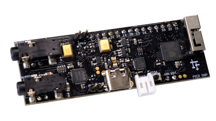
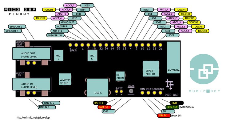
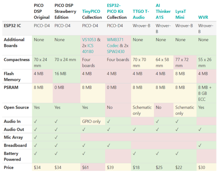
Pico DSP is built around an Espressif ESP32 PICO D4 processor, with a 32-bit dual-core microcontroller operating at 80/160/240 MHz. It provides a choice of either 4 MB SPI Flash with 8 MB additional pseudo-static RAM (PSRAM) or 16 MB of External SPI Flash.
Onboard there is a Wolfson WM9878 stereo audio codec with 3.5mm audio input and output connectors optimized for mobile computing and communications. Additionally, there are two on-board Knowles MEMS microphones that can be used as broadside or end-fire beam-forming arrays, as well as a stereo line-in and mono audio out on the GPIO header. The GPIO header also houses a 1W onboard speaker driver.
The development board is lightweight and portable. When combined with an external 3.7 V rechargeable Lithium-Polymer battery, it can be deployed practically anywhere or integrated into almost any device, instrument, or installation.
With a 70 x 24 mm form factor, the breadboard-friendly design includes 11 GPIO pins with access to both ESP32 ADC channels, JTAG for debugging, and capacitive-touch pins. For data and power, there is also a USB Type-C port. The manufacturer rates the board at 100mA while Wi-Fi is turned off and the microphones are active and under DSP control. Furthermore, it rates 52.4mA when the audio codec is on standby, and 5.7mA when the ESP32 is in deep sleep mode.
Talking about software support, PICO DSP supports several programming environments. Therefore, the board can be programmed in C/C++ with the Arduino IDE, Espressif IDF, or the open-source PlatformIO IDE extension for VS Code. Also, by using Esptool.py, you can flash it.
Original Edition vs Strawberry Edition
The firm recommends the Original Edition for beginner users who want to get started with audio programming on the ESP32 and are programming with the Arduino IDE. On the other hand, the “Strawberry Edition,” is a more experimental option for all those who require greater storage capacity.
Application Aspects of PICO DSP
In addition to DSP applications, the board can be used in different areas such as music, art, creative technology, and adaptive technology. Digital music synthesis, mobile recording, Bluetooth speakers, wireless line-level directional microphones, and the design of smart musical instruments are few examples of music-related technology. Art-related applications include acoustic sensor networks, sound-art installations, and Internet-radio applications. Examples of creative and adaptive technology are voice user interface (VUI) design and Web audio for the Internet of Sounds.
For more information on the PICO DSP open-source development board visit the Crowd Supply website.
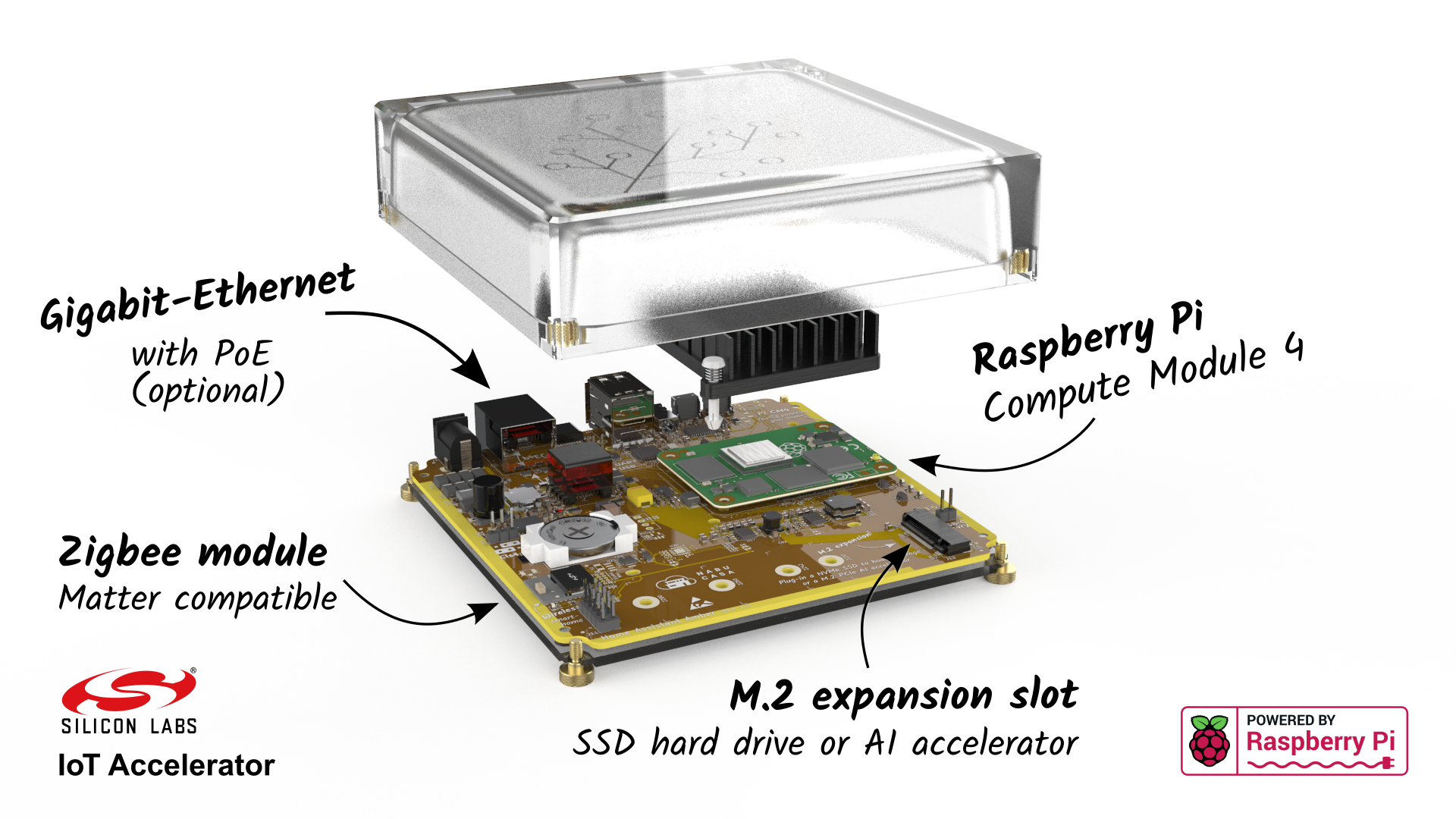
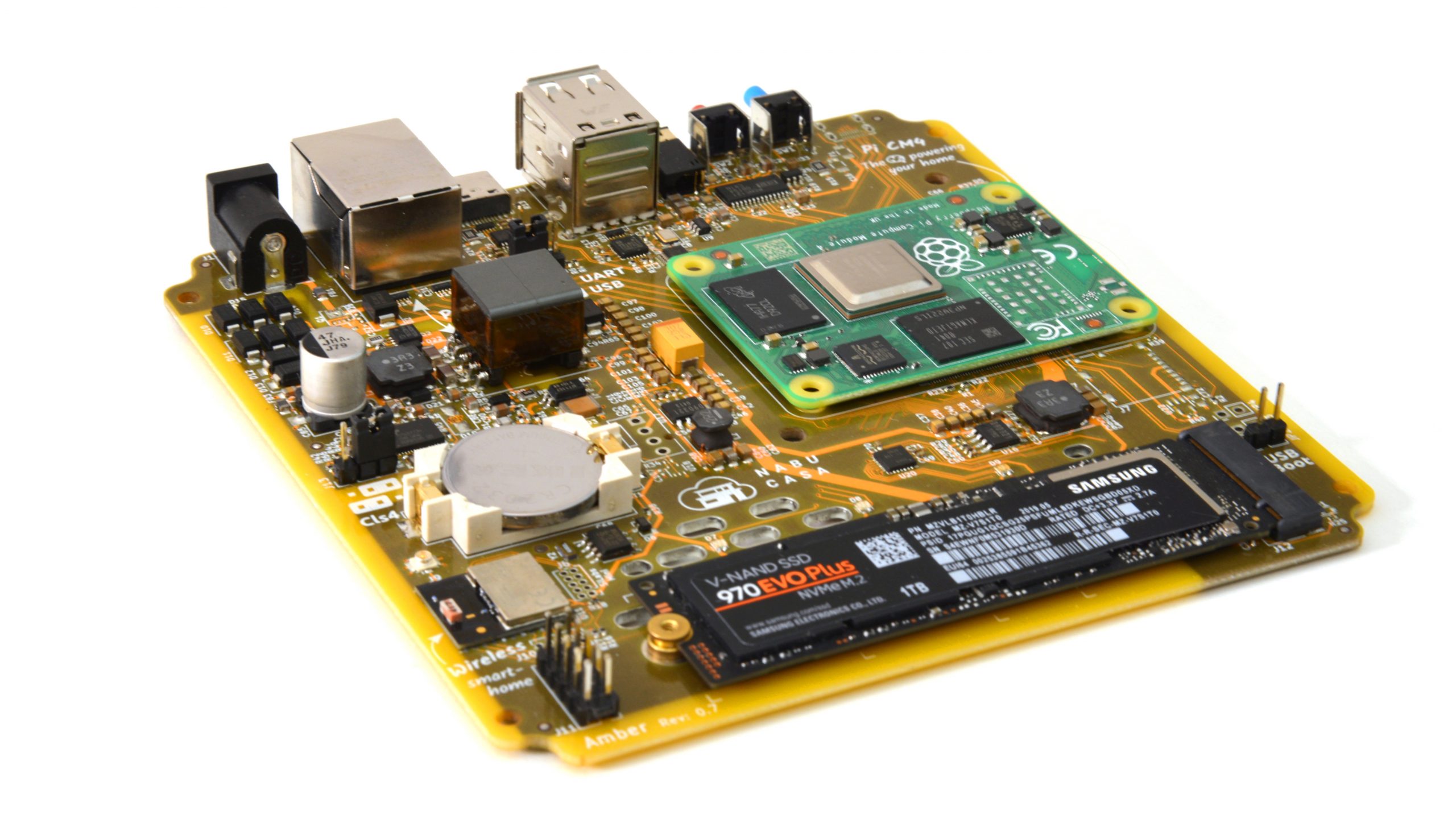
Crowd Supply, the leading product development platform connecting hardware creators with early adopters and enthusiastic backers, announces the launch of Home Assistant Amber, a purpose-built hardware solution for the operation of home automation software. Built by the developers of the popular Home Assistant software ecosystem, Amber offers a privacy-focused, open-source alternative to proprietary platforms like Google Home and Philips Hue. Home Assistant Amber is ready to work out of the box and boasts more than 1,000 integrations for unifying networks of smart home products including Nest, Sonos, and Amazon Alexa.
Features & Specifications
Carrier board for Raspberry Pi Compute Module 4 (CM4)
CM4 board-to-board connector
Supports direct boot from NVMe devices (e.g., for CM4 Lite)
12 cm x 12 cm
Compatible with all 32 variants of CM4
Quad-core Cortex-A72 (ARMv8) 64-bit / 1.5 GHz
Up to 8 GB RAM
Up to 32 GB eMMC
Regulatory approval does not cover wireless variants
Amber, developed by the makers of Home Assistant and launched with support from Crowd Supply as part of the Silicon Labs IoT Accelerator, is designed around the Raspberry Pi Compute Module 4, which can be easily upgraded to scale alongside your home automation needs. The new Home Assistant hardware device communicates with other devices using an integrated Zigbee radio by Silicon Labs, offering a forward-compatible solution with the Matter home automation protocol. Home Assistant Amber also features an onboard M.2 slot to facilitate expanded SSD storage or other peripherals.
Home Assistant Amber is available in three configurations. The flagship version operates immediately after plugging in the Ethernet cable and power supply, and the package includes a pre-installed Raspberry Pi Compute Module 4 (CM4). Another kit is a suitable option for those who already own a CM4, as it features all other necessary components for operation, including a CM4 carrier board, heat sink, transparent polycarbonate enclosure, power supply, and Ethernet cable. Finally, a PoE kit features a Power-over-Ethernet-enabled CM4 carrier board for single-wire operation.
Fibocom, a global leading provider of IoT (Internet of Things) wireless solutions and wireless communication modules, introduces the LTE Advanced wireless module FM101-CG. Featuring 3GPP Release 12 capabilities, the FM101-CG module is exclusively designed to boost the commercial deployment of products operating in the US Citizen Broadband Radio Service (CBRS) spectrum.
To relieve the difficulty and uncertainty people faced in the ongoing COVID-19 pandemic, the US Federal Communications Commission (FCC) has announced a $7.17 billion Emergency Connectivity Fund Program, which aims to help students, school staff and library patrons improve internet connectivity using the CBRS band for remote learning. CBRS, shared spectrum from 3.55 to 3.7 GHz, is able to offer fast connectivity in the US with the reliability that sophisticated educational applications demand.
Fibocom is accelerating CBRS-based wireless network deployment with our new LTE-A Category 6 wireless communication module FM101-CG. It is able to address the requirements of CBRS-based network applications for multiple scenarios, including but not limited to remote education, industry IoT, smart cities, etc. Powered by the Snapdragon® X12+ LTE Modem from Qualcomm Technologies, Inc., Fibocom’s FM101-CG module supports LTE TDD Band 42/43/48 and delivers maximum data rates of up 260 Mbps downlink and 30 Mbps uplink. The module adopts M.2 form factor measuring 30.042.02.3mm.
Along with abundant functionalities such as DFOTA, VoLTE and Audio, the Fibocom FM101-CG module supports multi-constellation GNSS receiver, including GPS, GLONASS, BeiDou and Galileo, for high-performance positioning and navigation. Fibocom’s FM101-CG module supports multiple operating systems (Linux/ Android/ Windows), various Internet protocols as well as a rich set of digital interfaces (USIM, USB 3.0/2.0, PCIe 2.0 and PCM/I2S), allowing much flexibility and ease of integration for customer’s application.
“Qualcomm Technologies is pleased to collaborate with Fibocom on the introduction of the FM101-CG module, featuring the Snapdragon X12+ LTE Modem. Qualcomm Technologies has been at the forefront of commercialization of CBRS with support since 2017 and this announcement further emphasizes our commitment to the wide scale deployment of CBRS and enabling reliable, cost-effective and scalable wireless connectivity that addresses the sophisticated needs of remote education, small businesses, hospitals, industry IoT, homes and more,”
said Gautam Sheoran, Senior Director, Product Management, Qualcomm Technologies, Inc.
Ron Friedman, VP of Americas Sales Dept., Fibocom, commented,
“Powered by the Snapdragon X12+ LTE Modem, the Fibocom FM101-CG module is tailored for CBRS network, providing seamless and reliable connectivity for various industries. With shared spectrum technology CBRS, organizations can make use of their own private networks, particularly for off-campus connectivity, ensuring fast, reliable and secure connectivity that’s available in limited, hard-to-reach areas.”
At present, the engineering samples of FM101-CG are available for product testing and development, which provides solutions that helps device OEMs and systems designers with their innovative new products, optimizing business operations and processes.
The digital buffers are used in digital circuits for the amplification of digital signals in order to drive high current loads. Besides current amplification, the digital buffers provide isolation between input and output circuits where output is connected to some high-power load such as a relay, lamp or solenoid, etc. The digital device used for such purposes is called Digital Buffer.
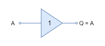
The digital buffer is similar to the logic “NOT” gate in a way that it is a two-terminal device having input and output terminals only. However, the logic “NOT” gate complements the input signal at its output. As discussed in the logic “NOT” gate article, when the input of a “NOT” gate is “HIGH” then its output will NOT be “HIGH”. Likewise, when the input of a “NOT” gate is “LOW” then its output will NOT be “LOW”. On the other hand, the digital buffer does not complement the input signal at its output. The input signal is reflected at the output of a digital buffer without any change in its logic. The digital buffer is a non-inversion logic and follows Idempotent Law. Its Boolean expression is given below:
Q = A
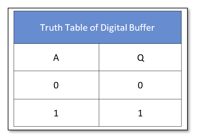
From the expression, it is eminent that the output (Q) state of a digital buffer is only true when the input (A) is true otherwise the output (Q) is false. The symbol and truth table of a digital buffer is shown below:
Figure 1: Digital Buffer symbol
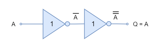
Construction using NOT Gates
The digital buffer can be constructed using a basic logic “NOT” gate. The connection of two logic “NOT” gates back-to-back in series form a Digital Buffer. First, the “NOT” gate inverts the input signal, and second, “NOT” inverts the inverted signal back to the original input signal. The process of “double inversion” leads to the formation of a Digital Buffer.
Figure 2: Digital Buffer constructed using logic “NOT” gates
Digital Buffer Fan-out
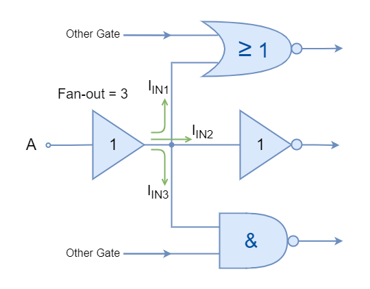
The Digital Buffer is used in digital circuits even though it does not perform any logic or decision. The Digital Buffer is useful in the isolation or separation of two circuits whereas the impedance of the input circuit does not affect the impedance of the output circuit. Moreover, it can be used to drive high current loads such as switches or relays, etc. This means that Digital Buffers have the “fan-out” capability to deliver high power to the output loads.
The “fan-out” is the ability of a Digital Buffer or Digital I.C. to deliver high output current to a load. It is simply, the capability to amplify the input signal at its output after performing any due logic. The output of a logic gate may need to be connected to a high current LED, switch or relay and in such a case a logic gate with a high “fan-out” is required. Usually, the output of a logic gate is connected to the input of another logic gate and it requires a nominal current to drive another gate’s input. When a number of inputs (logic gates) are connected to the output of a logic gate then additional current is required which depends upon a number of factors such as the number of inputs and their circuit types etc. In simple words, it can be said that the “fan-out” is the number of parallel connections that can be efficiently driven by a logic gate or Digital Buffer.
Figure 3: “Fan-out” example using a Digital Buffer
Generally, a Digital Buffer can have a high “fan-out” rating of 20 to drive parallel connections of the same logic family. A Digital Buffer with a high fan-out (current source) rating also carries a high fan-in (current sink) rating. However, there is a limitation to the number of devices that can be connected to the input or output of a logic gate due to propagation delay. The propagation delay is a function of the number of connections taken out of a terminal and it deteriorates with the increase in the number of signals.
Tri-state Buffer
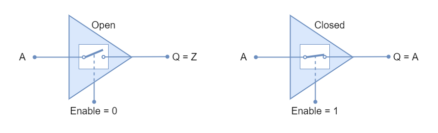
The Tri-state Buffer, as the name says, has three states that can be achieved by an electronic controller connected to an input terminal of Digital Buffer. The Tri-state Buffer is used in circuits where decoupling of input and output circuits is essentially required. It is a device similar to the Digital Buffer but has three terminals and the additional (third) terminal is used to control the output of Digital Buffer. Additionally, it has three states compared to the two states of a Digital Buffer.
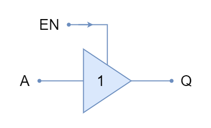
The Tri-state Buffer’s output (Q) can be put into any of the three states by electronically driving its “Control” or “Enable” terminal to logic “LOW” or “HIGH”. It can be thought of as an input controller switch which is demonstrated in the following figure.
Figure 4: Tri-state Buffer states
The Tri-state buffer can be activated or deactivated using the “Enable” terminal. When enabled, the Tri-state Buffer reflects the input signal towards the output without any change just like a Digital Buffer. Whereas, when Tri-state Buffer is disabled then path between input and output becomes open-circuited and leads to a high impedance state “Hi-Z”. This high impedance state “Hi-Z” is the third-state besides logic “HIGH” and “LOW” states. Because of these three states, it is called a Tri-state Buffer.
In the high impedance “Hi-Z” state, a high impedance appears between input and output leading to electrical isolation. In this state, no current flows in the input and from the output.
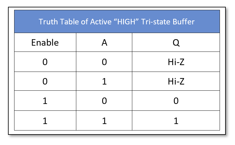
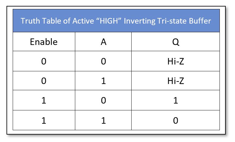
The Tri-state Buffer discussed above is an Active “HIGH” Tri-state Buffer as it becomes active when “Enable” is at a “HIGH” state. Another variant is an Active “LOW” Tri-state buffer which gets activated when “Enable” is at a “LOW” state. These Tri-state Buffers are non-inverting when enabled and reflect the input signal at the output without inversion. However, Tri-state inverting Buffers are also commercially available which inverts the input signal at the output. They are also available in Active “HIGH” inverting and Active “LOW” inverting Tri-state Buffer variants. These four types of Tri-state Buffer variants are explained below along with their truth tables.
Active “HIGH” Tri-state Buffer
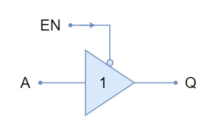
The symbol and truth table of Active “HIGH” Tri-state Buffer is shown below:
Figure 5: Active “HIGH” Tri-state Buffer
The active “HIGH” Tri-state Buffer is commercially available as 74LS241 with octal buffers. It is active when the “Enable” terminal is at a “HIGH” state and passes the input signal towards the output unaltered. When the “Enable” terminal is at the “LOW” state then Tri-state Buffer becomes disabled and a high impedance state “Hi-Z” appears at the output.
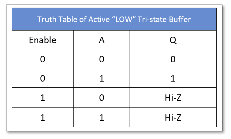
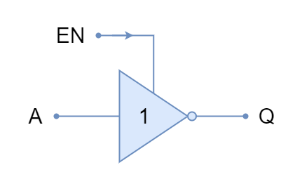
Active “LOW” Tri-state Buffer
The symbol and truth table of Active “LOW” Tri-state Buffer is shown below:
Figure 6: Active “LOW” Tri-state Buffer
The active “LOW” Tri-state Buffer is active when the “Enable” terminal is at a “LOW” state and passes the input signal towards the output unaltered. When the “Enable” terminal is at the “HIGH” state then Tri-state Buffer becomes disabled and a high impedance state “Hi-Z” appears at the output. The “Inversion Bubble” at the terminal of “Enable” indicates an active “LOW” input.
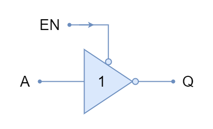
Active “HIGH” Inverting Tri-state Buffer
The symbol and truth table of Active “HIGH” Inverting Tri-state Buffer is shown below:
Figure 7: Active “HIGH” inverting Tri-state Buffer
The active “HIGH” Tri-state Buffer is commercially available as 74LS240 with octal buffers. It is active when the “Enable” terminal is at a “HIGH” state and passes the input signal towards the output after inversion. When the “Enable” terminal is at the “LOW” state then Tri-state Buffer becomes disabled and a high impedance state “Hi-Z” appears at the output. The “Inversion Bubble” at the output terminal indicates an inversion of the input.
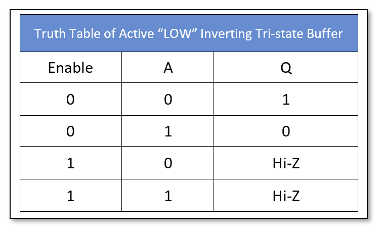
Active “LOW” Inverting Tri-state Buffer
The symbol and truth table of Active “LOW” Inverting Tri-state Buffer is shown below:
Figure 8: Active “LOW” inverting Tri-state Buffer
The active “LOW” Tri-state Buffer is active when the “Enable” terminal is at a “LOW” state and passes the input signal towards the output after inversion. When the “Enable” terminal is at the “HIGH” state then Tri-state Buffer becomes disabled and a high impedance state “Hi-Z” appears at the output. The “Inversion Bubble” at the output terminal indicates an inversion of the input. Whereas, “Inversion Bubble” at the terminal of “Enable” indicates an active “LOW” input.
Tri-state Buffer as Bus Controller
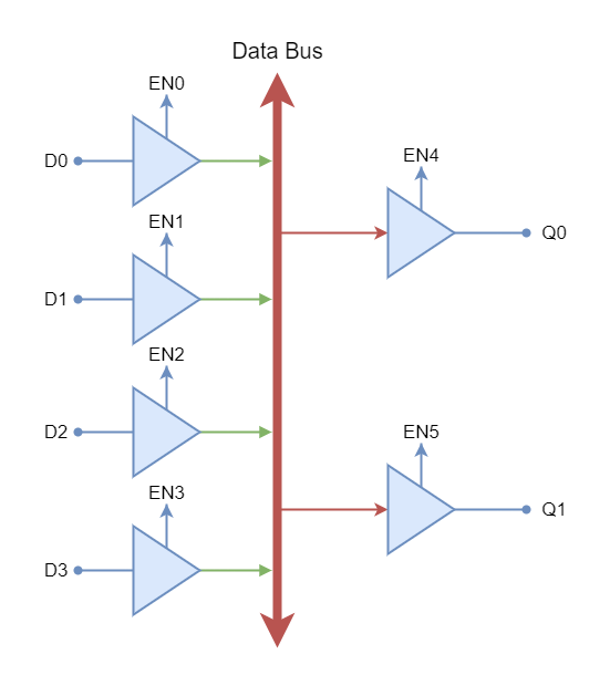
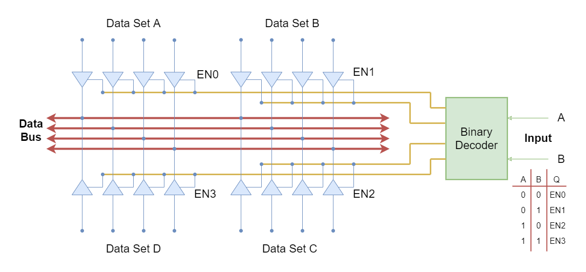
The Tri-state Buffers are used in many electronic and digital circuits to control access to the data buses allowing multiple devices to be connected to the single data bus. The data buses exist between microprocessors, peripherals, I/O or memory chips, etc. and multiple devices interface with them. The multiple devices connected with the same bus tries to fetch the bus to “LOW” or “HIGH” creating a contention. The contention is said to occur when some of the devices try to pull up (HIGH) the bus whilst at the same time some devices try to pull it down (LOW). This would create a condition of short-circuiting and could cause damage to the delicate circuitry. The Tri-state Buffer is used to control the interface/ access between the device and bus. It connects or isolates the interface using the “Enable” line and connects the desired device at a time to the bus. In the following figure, a common data bus is connected to the four data-in lines and two-bit data-out lines.
Figure 8: Data Bus access example using Tri-state Buffers
Using “Enable” lines of four data-in lines, any one of them can be connected to the data bus and its desired output (data-out) can be selected in a similar way. In this scheme, a total of six devices are connected to the common data bus and each of them can utilize this bus to route their data to different devices/ peripherals at the output.
Tri-state Buffer Control
The multiple Tri-state Buffers can be controlled using a digital decoder. The digital decoder, such as a Binary Decoder, has a number of binary inputs and selects the appropriate decoder output depending on the binary input signals. The Tri-state Buffers connected to that specific decoder output becomes active only whilst others remain at the “Hi-Z” state. Another state of binary inputs leads to a change in decoder output and another set of Tri-state Buffers interfaces the data bus. Meanwhile, other Tri-state Buffers become isolated. In the following figure, a 4-bit data bus is shown to be connected with four different data sets using a binary decoder.
Figure 9: A 4-bit data bus interface example using Tri-state Buffers
In the above figure, Data Set A gets connected to the common data bus when inputs are at state “00”. In the same way, Data Sets B, C, and D make an interface with the bus when inputs are at “01”, “10”, and “11” states, respectively.
Commercially Available Buffers
CMOS based Buffers
CD4050 Hex Non-inverting Buffer
CD4503 Hex Tri-state Buffer
TTL based Buffers
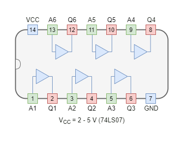
74LS07 Hex Non-inverting Buffer
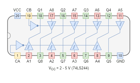
74LS244 Octal Buffer
In the following figures, a Digital Buffer (74LS07) and Octal Tri-state Buffer (74LS244) are shown.
Figure 10: TTL “74LS07” HEX Digital Buffer packageFigure 11: TTL “74LS24” Oct Tri-state Buffer package
Conclusion
The Digital Buffer is a simple two-terminal device that is used for the amplification of digital signals.
The Digital Buffer isolates the input and output circuits so that their impedances do not affect each other.
The Digital Buffer can be non-inverting or inverting and, in the case of inverting, an inverted signal of input appears at the output.
The Digital Buffers have high “fan-out” and “fan-in” capability which means that a number of devices can be connected at the input and output. Because of the high “fan-out” (current source) rating, a high current LED, switch, or relay can be driven through it.
The Tri-state Buffer has an additional input terminal called “Enable” and a high impedance state “Hi-Z” compared to the Digital Buffer.
The Tri-state Buffer output can be controlled through the “Enable” line leading to coupling and decoupling of input and output circuits. In disable or decouple state, a high impedance state (Hi-Z) appears between input and output terminals of the Tri-state Buffer.
The Tri-state Buffers are commercially available in Active “HIGH” Non-inverting, Active “LOW” Non-inverting, Active “HIGH” Inverting, and Active “LOW” Inverting variants.
The Tri-state Buffers are used in microprocessors or digital circuits to control the interfaces of data buses between devices.
The Tri-state Buffers control can be driven using a Decoder which enables or disables a set of Tri-state Buffers depending upon the decoder output.
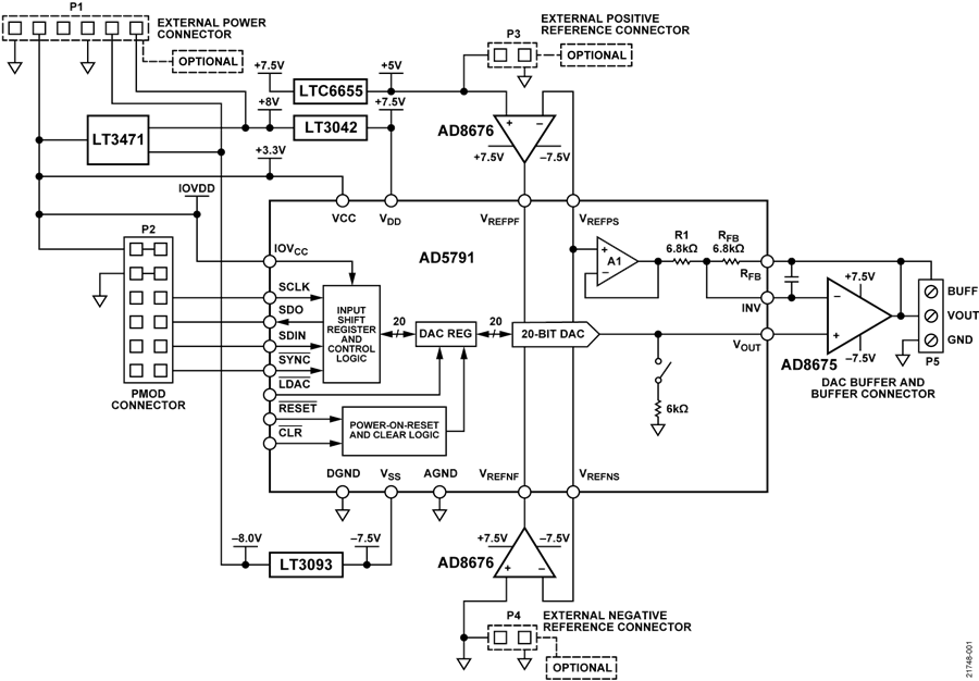
Precision dc voltages are a critical component of scientific instrumentation and measurement equipment, automated test equipment, factory automation and control, chemical analysis, and many other high precision applications. The most demanding applications require single digit, part per million temperature drift, subppm linearity, and low, predictable noise performance.
The circuit shown in Figure 1 is a programmable 20-bit voltage source that enables these demanding applications. The output range is −5 V to +5 V with ±1 LSB integral nonlinearity (INL), ±1 LSB differential nonlinearity (DNL), and exceptionally low noise and low drift across the entire output range.
On-board power converters produce the required supply rails from a single voltage supply provided by the development platform board. Low noise, high power supply rejection ratio (PSRR) voltage regulators ensure that the switching noise is minimized. A high precision, high stability, on-board hermetically sealed voltage reference ensures the high precision and accuracy of the 20-bit system.
Features:
+/-5V Output Range
20-Bit Signal Generation Control
On board precision 5V Reference
All Power Rails Generated Using a Single 3.3V Source
The output of the circuit is a buffered voltage with an option for a remote sense connection to compensate for lead resistance or allow for the insertion of an external power stage, if necessary, providing drive flexibility for the desired end application.
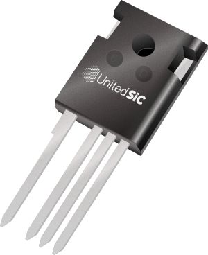
At an RDS(on) value of less than half the nearest SiC MOSFET competitor, a new 6-mΩ device also provides a robust short-circuit withstand time rating of 5 μsec. The new 750-V SiC FET series includes nine new device/package options rated at 6, 9, 11, 23, 33, and 44 mΩ. All devices are available in the TO-247-4L package while the 18, 23, 33, 44, and 60 mΩ devices also come in the TO-247-3L. Complemented by the already available 18 and 60-mΩ devices, this 750-V expanded series provides designers with more device options, enabling more design flexibility to achieve an optimum cost/efficiency trade-off while maintaining generous design margins and circuit robustness.
Gen 4 SiC FETs from UnitedSiC are a ‘cascode’ of a SiC JFET and a co-packaged silicon MOSFET. These together provide the full advantages of wide band-gap technology–high speed and low losses with high-temperature operation, while retaining an easy, stable, and robust gate drive with integral ESD protection. The advantages are quantified by Figures of Merit (FoMs) such as RDS(on)xA, a measure of conduction losses per unit die area. Gen 4 SiC FETs achieve the lowest values in the market at both high and low die temperatures. FoM RDS(on)xEOSS/QOSS is important in hard-switching applications and is half the nearest competitor value. FoM RxCOSS(tr) is critical in soft-switching applications and UnitedSiC device values are around 30% less than competitor parts, rated at 650 V compared with UnitedSiC’s at 750 V.
For hard switching applications, the integral body diode of SiC FETs is superior in recovery speed and forward voltage drop to competing Si MOSFET or SiC MOSFET technologies. Other advantages incorporated into the Gen 4 technology are reduced thermal resistance from die-to-case by advanced wafer thinning techniques and silver-sinter die-attach. These features enable maximum power output for low die temperature rise in demanding applications.
With their latest improvements in switching efficiency and on-resistance, the new UnitedSiC SiC FETs are candidates for challenging, emerging applications. These include traction drives and on- and off-board chargers in electric vehicles and all stages of uni- and bi-directional power conversion in renewable energy inverters, power factor correction, telecoms converters and AC/DC or DC/DC power conversion generally. Established applications also benefit from use of the devices for an easy boost in efficiency with their backwards compatibility with Si MOSFET and IGBT gate drives and established TO-247 packaging.
Pricing (1000-up, FOB USA) for the new 750-V Gen 4 SiC FETs range from $4.15 for the UJ4C075044K3S, to $23.46 for the UJ4SC075006K4S. All devices are available from authorized distributors.
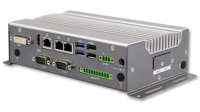
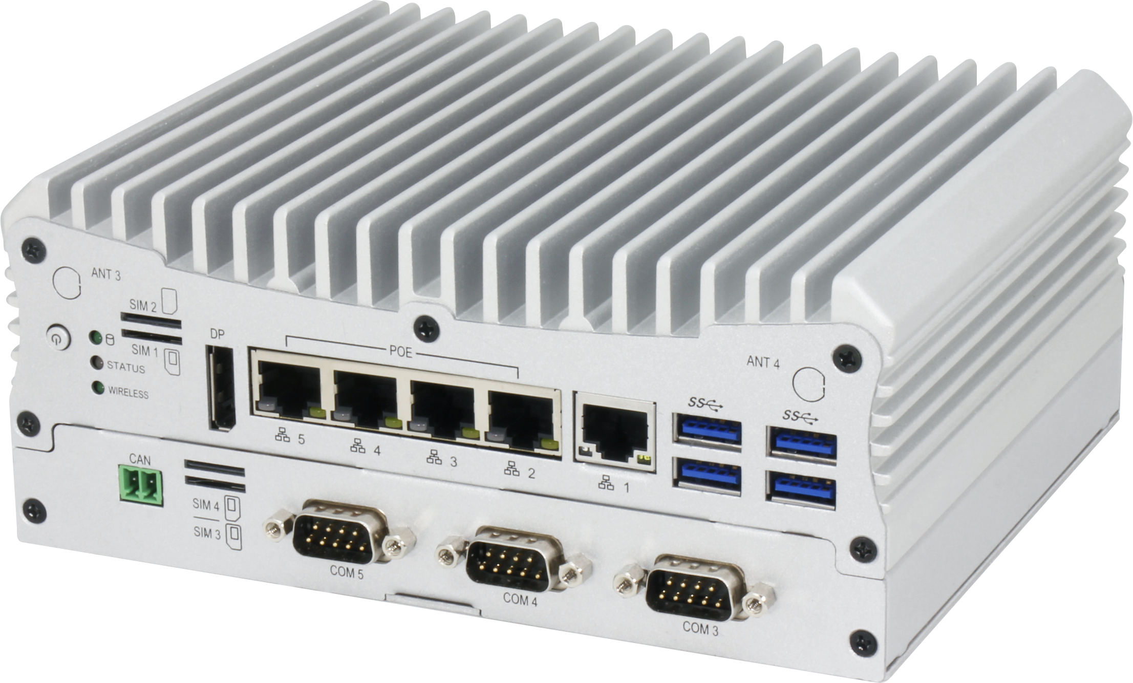
IBASE Technology Inc., a leading provider of industrial motherboards and embedded systems, rolls out AGS103T ultra-compact IoT gateway edge computing system integrating the Intel Atom® x6000E Series processors (code-named Elkhart Lake) that deliver up to 4 cores with 40% increase in CPU performance and improved graphics when compared with previous versions. Based on Intel’s 10nm technology, the energy-efficient platform is suitable for embedded applications in factory automation, IoT gateway, edge computing and automatic control systems.
The ruggedized AGS103T boasts several advanced features such as an extended operating temperature range of -20°C to 70°C, three Gigabit Ethernet ports for fast wired connections and multi-protocol communications, and over/under/reverse voltage protection. Useful I/O interfaces include 3042/2242 M.2 B-Key, Micro SD, four COM (RS232/422/485), two USB 3.1 and two USB 2.0 sockets.
In addition, the low-power AGS103T supports DIN-rail and wall mounting installation, and onboard TPM 2.0 hardware-based security to ensure platform integrity. It is available with Intel® Atom® QC x6413E or Intel® Atom® DC x6211E and with an option for additional storage for 2.5” drives. For more information, please visit www.ibase.com.tw.
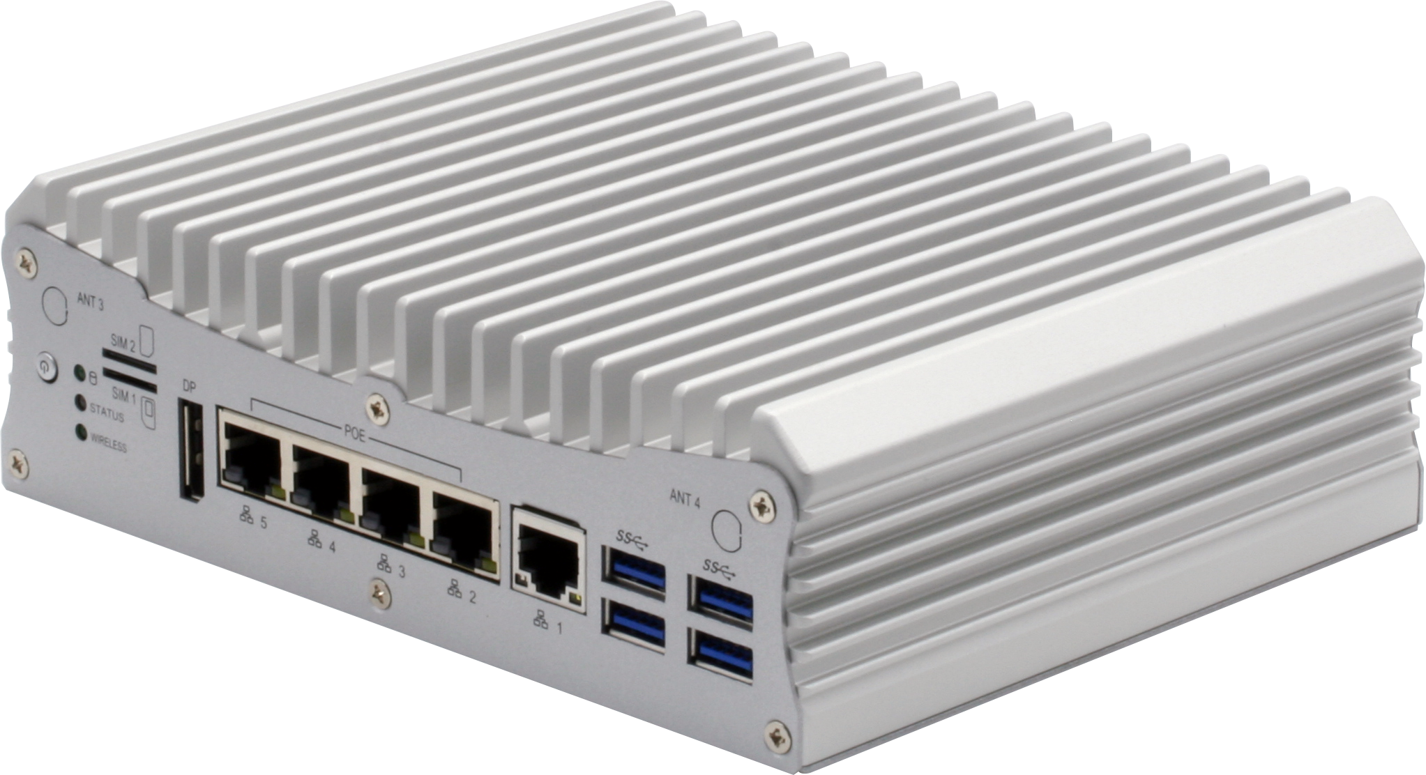
AAEON, a leader in embedded edge platforms, introduces the VPC-5620S industrial embedded system. Available in two builds, the slim VPC-5620S IS and in-vehicle VPC-5620S VS, the system leverages a modular design to combine the power 8th Generation Intel® Core™ processors with greater performance, storage capabilities and expansion support.
The VPC-5620S brings the performance of the 8th Generation Intel Core processors (formerly Whiskey Lake) to a rugged industrial platform designed to power embedded AI Edge applications anywhere they’re needed. With up to 64GB of memory, the VPC-5620S can power intelligent visual analysis applications such as Smart Factory and Security, and with expansion slots, can support AI accelerators to scale up the inference processing capabilities.
Available in two standard configurations, the VPC-5620S IS industrial system and VPC-5620S VS in-vehicle system, this versatile platform offers broad I/O features including four Smart PoE PSE ports designed for PoE cameras. Built to simplify the deployment of visual applications, the Smart PoE ports can be managed with a user-friendly interface, allowing users to control voltage outputs or turn ports on and off remotely. Additional I/O features include four USB3.2 Gen 1 ports, two COM ports, HDMI and 8-bit DIO. Thanks to the modular design of the VPC-5620S platform offers additional configurations available on a per-project basis.
The VPC-5620S offers expandability to help quickly add on functionality and storage flexibility. Wireless connectivity is supporting through two mPCIe slots, designed for Wi-Fi and LTE network deployments, along with an optional M.2 slot for 5G support. The system offers and M.2 slot with NVMe support for fast read/write speeds, as well as two 2.5” SATA drive bays in standard configuration to support local network storage needs, such as for NVR and AI Surveillance applications. Users can also utilize eMMC and mSATA storage options.
One key feature of the VPC-5620S is its rugged design. Built to operate in a wide range of environments, the system boasts an operating temperature range of -20°C to 70°C. The system is tested to MIL-STD-810G shock and vibration standards, and the fan-less design helps keep dust and contaminants out, ensuring long-lasting, consistent and reliable operation. Additionally, the VPC-5620S comes standard with wide voltage input, supporting 12 – 24V inputs.
With its modular design, the VPC-5620S platform delivers a range of flexibility unlike other systems. In addition to the standard VPC-5620S IS and VPC-5620S VS systems, the VPC-5620S offers several optional configurations. AAEON offers additional service and support to help provide customization and configuration support to users and developers, helping meet the exact needs of their applications.
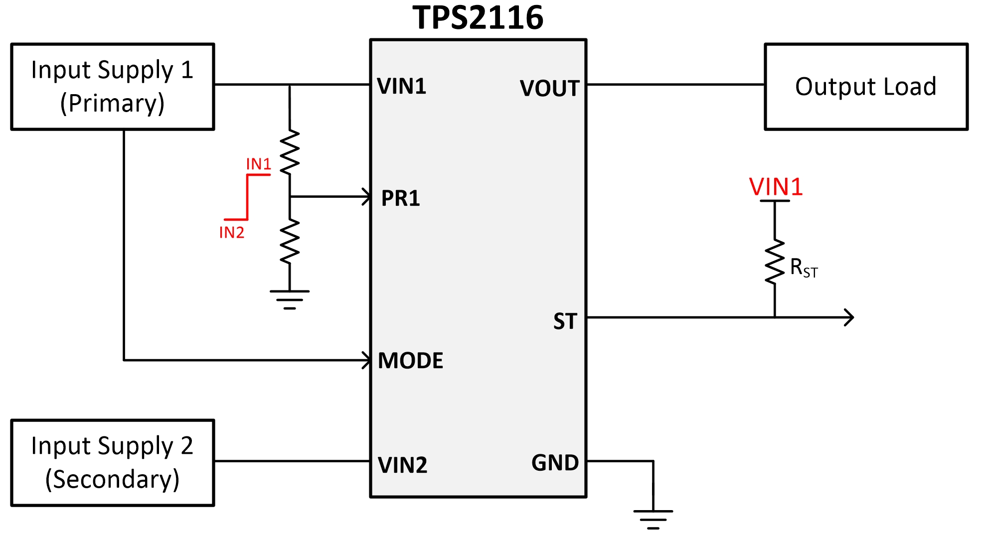
Texas Instruments’ power mux features manual and priority switchover
Texas Instruments TPS2116 is a power mux device with a voltage rating of 1.6 V to 5.5 V and a maximum current rating of 2.5 A. The device uses N-channel MOSFETs to switch between supplies while providing a controlled slew rate when voltage is first applied.
The low quiescent of 1.32 µA (typical) and a low standby current of 50 nA (typical) make the TPS2116 ideal for systems where a battery is connected to one of the inputs. These low currents extend the life and operation of the battery when in use. The TPS2116 can be configured for two different switchover behaviors depending on the application. Automatic priority mode prioritizes the supply connected to VIN1 and switches over to the secondary supply (VIN2) when VIN1 drops. Manual mode allows the user to toggle a GPIO or enable a signal to switch between the channels.
Features
Input voltage range: 1.6 V to 5.5 V
Continuous current: 2.5 A (max.)
On resistance: 40 mΩ (typ.)
VIN2 standby current: 50 nA (typ.)
Quiescent current: 1.32 µA (typ.)
Thermal shutdown
Switchover modes: priority mode and manual mode
Controlled output slew rate: 1.3 ms (typ.) at 3.3 V
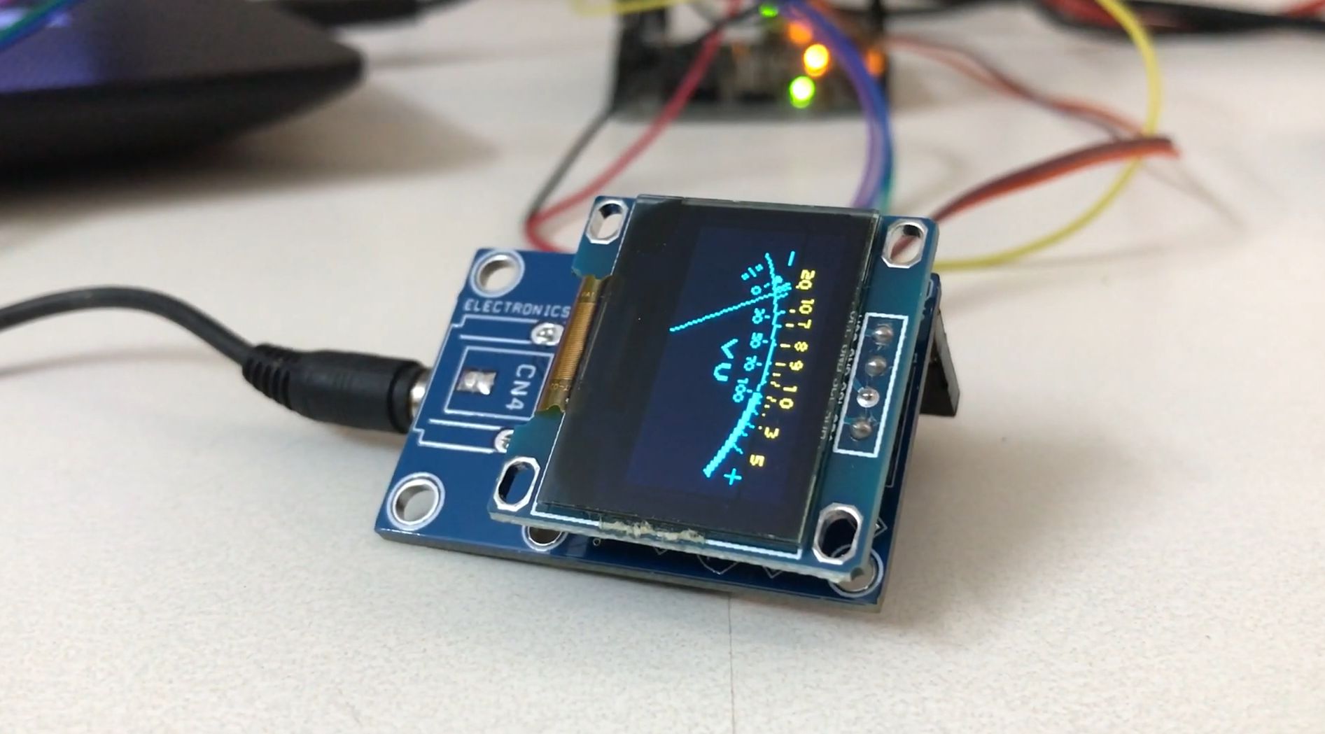
This is an analog-style VU meter on a 0.96″ OLED Display. The project has a 0.96″ OLED display, Atmega328 Microcontroller, 3.5 mm audio EP socket for audio signal input. This Arduino compatible hardware can be program using Arduino IDE. Operating Supply 5V DC.
Analog Style VU Meter on OLED Display – Arduino Compatible – [Link]