Epishine signs distribution agreement with Farnell to enable light energy harvesting within electronic design

Epishine’s new-to-market printed organic solar cells and development kits remove the need for batteries reducing the impact on the environment.

The innovative Swedish manufacturer of printed organic solar cells and development kits Epishine has signed a new franchise agreement with Farnell, an Avnet Company and global distributor of electronic components, products, and solutions. The new-to-market printed organic solar cells are optimized for harvesting energy from indoor, low energy lighting enabling organic solar power to be used everywhere. Design engineers can utilize this new and innovative technology with Epishine’s Light Energy Harvesting Evaluation Kit. Farnell is the first high-service distributor to stock products from Epishine.

Epishine’s organic solar cells are small, thin, flexible, and printed on recyclable plastic. The cells can be easily integrated into any low-power electronic equipment where they convert ambient indoor light into electricity. New product designers can replace batteries in wireless sensors and similar devices with organic solar cells, reducing the environmental impact of battery waste and saving battery replacement costs.

The Light Energy Harvesting Evaluation Kit (EK01LEH3_6) demonstrates how Epishine’s Light Energy Harvesting (LEH) modules can power indoor wireless low-power devices that are usually powered by batteries. It combines a 6-cell 50x50mm LEH module with a supercapacitor which acts as an energy buffer and intelligent charging management system to support various output voltages and energy storage solutions. It can even use an external primary battery as a backup. The evaluation kit can deliver sufficient output current to power most low-power wireless devices such as BLE, Zigbee, and LoRa. The ability to program the evaluation kit provides added flexibility and showcases the unique product integration and design possibilities of Epishine’s LEH modules.

Key features include:

  • Selectable output voltage ranging from 1.8V to 3.3V in 0.1V steps
  • Up to 300mA output current
  • Optimized for indoor use (-20°C to 40°C / 0-85%RH) with illumination intensities of 20 to 1000 lux
  • A supercapacitor for energy storage which can be reconfigured to charge rechargeable battery

Epishine’s organic solar cells will be added to Farnell’s line card later this year. Epishine’s Light Energy Harvesting Evaluation Kit is now available for fast delivery from Farnell and Newark in North America.

230V AC Input – 12V Output DC Converter, Non-Isolated Buck Converter

The project described here outputs 12V DC voltage from the input of 230V AC. The output current is up to 100mA.  The project is based on BM2P129TF chip which is PWM method DC/DC converter with a built-in 650V MOSFET. BM2P129TF contributes to low power consumption by built-in a 650V starting circuit. Built-in current detection resistor realizes compact power supply design. Current mode control imposes current limitation on every cycle, providing superior performance in bandwidth and transient response. The switching frequency is 100Khz in fixed mode. At light load, frequency is reduced and high efficiency is realized. Built-in frequency hopping function contributes to low EMI. Low on-resistance 9.5 Ohms 650V MOSFET built-in contributes to low power consumption. The default over current limit of the chip is 450mA.

This project uses lethal AC voltage and should be handled only by qualified personnel familiar with all safety and operating precedes.
Note: The project can also operate with a lower input voltage of 90V AC. The board provides 10.5V and load current 2mA with 90V AC input. The module also can be used as a high voltage DC-DC to DC converter with input range 100V DC to 380V DC, output 10.5V to 13V.

Features

  • Input Supply 230V AC
  • Output 12V DC
  • Load 100mA Constant (Maximum 150mA)
  • Operating Frequency 100kHz Fixed
  • Cycle By Cycle Current Control
  • Efficiency 75%
  • PCB Dimensions: 46.67 x 19.53 mm

Schematic

Connections


Parts List

NOQNTYREFDESCMANUFACTURERSUPPLIERSUPPLIER PART NO
11CN12 PIN SCREW TERMINAL PITCH 5.08MMPHOENIXDIGIKEY277-1247-ND
21CN24 PIN HEADER CONNECTOR PITCH 2.54MMWURTHDIGIKEY732-5317-ND
31C11uF/25V SMD SIZE 0805YAGEO/MURATADIGIKEY
41C2220uF/25V ELECTROLYTICNICHICONDIGIKEY493-15302-ND
51C30.1uF/50V SMD SIZE 0805YAGEO/MURATADIGIKEY
61C44.7uF/400V ELECTROLYTICWURTHDIGIKEY732-8886-1-ND
71D11N4007MICRO COMMERCIALDIGIKEY1N4007MSCT-ND
81D2MDB10SONSEMIDIGIKEYMDB10SFSCT-ND
91D3BA159VISHAYDIGIKEYBA159GP-E3/73GICT-ND
101L1220uH/1.38ABOURNSDIGIKEY118-SRR1260A-221KCT-ND
111R11E 2W SMD SIZE 2512YAGEO/MURATADIGIKEY118-SRR1260A-221KCT-ND
121R210K 5% SMD SIZE 0805YAGEO/MURATADIGIKEY
131U1BM2P129TF SOIC8ROHMDIGIKEYBM2P129TF-E2CT-ND

Gerber View

Photos


Video

BM2P129TF Datasheet

Prodigy PGY-LA-EMBD Logic Analyzer Hands-on Review

Prodigy Logic Analyser

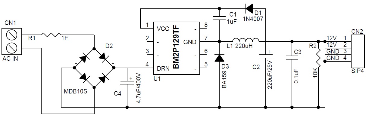
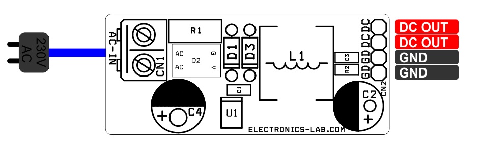
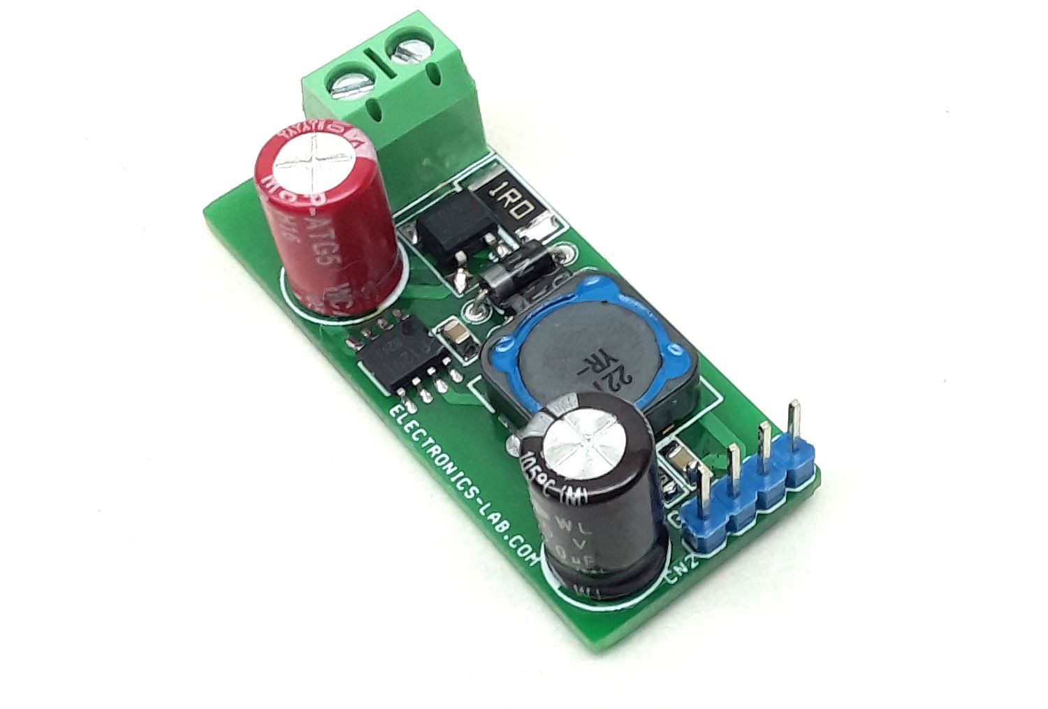
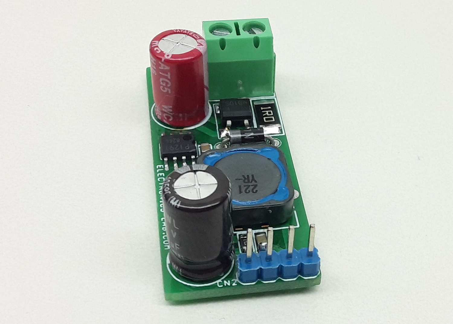
Since its introduction in 1973 by Hewlett Packard, Logic Analyzers have been one of the most important tools in an engineer’s toolkit. Logic Analyzers enable us to easily debug digital logic signals by capturing the data and plotting it in a time-view format. They serve a similar purpose as an oscilloscope, which is a tool to view analog waveforms. With the advancements in technologies, circuits are becoming much faster and more complex and thus require a high sampling rate to be debugged properly. This created a demand for easy-to-use Logic Analyzers with high speed and low cost, giving rise to surprisingly good USB-based analyzers. In this article, we’ll have a hands-on look at one such Logic Analyzer from Prodigy Technovations, which can provide 1GS/s sampling speed that too on all of its 16 channels.

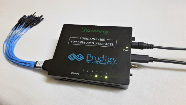
Prodigy Technovations, the leading provider of innovative protocol analysis solutions, designed and manufactured the Logic Analyzer for Embedded Interfaces. Also identified as PGY-LA-EMBD, these Logic Analyzers can even work as a Protocol Analyzer or both simultaneously. So let’s jump into the review now.

Accessories in the box and build quality

The packaging was quite well done, with all the electronics placed inside anti-static plastic bags. There were a total of five components, including the Logic Analyzer. The very first thing we get our eyes on is the custom 16-channel flying lead probe cable. There are 16 pairs of wires, each pair consisting of a digital wire and a ground wire. The cables are labeled with their corresponding channel number, which is very convenient while connecting to the interface to be debugged. The cable is well insulated with heat shrinks at every pair and surely comes under high quality. Next, we get a C-Type USB cable that is noticeably thicker than the normal ones and a 12W 5V DC power adapter to power the device. In addition to the above, there was also a CD with a software setup and user manual in it.

Prodigy Logic Analyser Hands-on Review Components


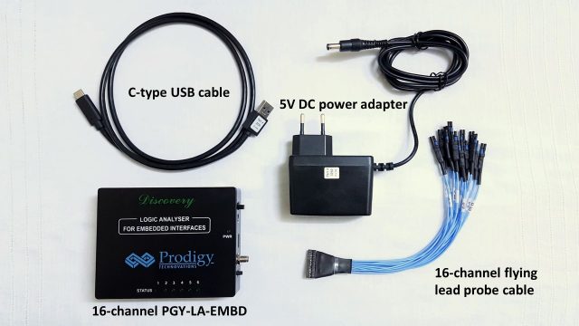
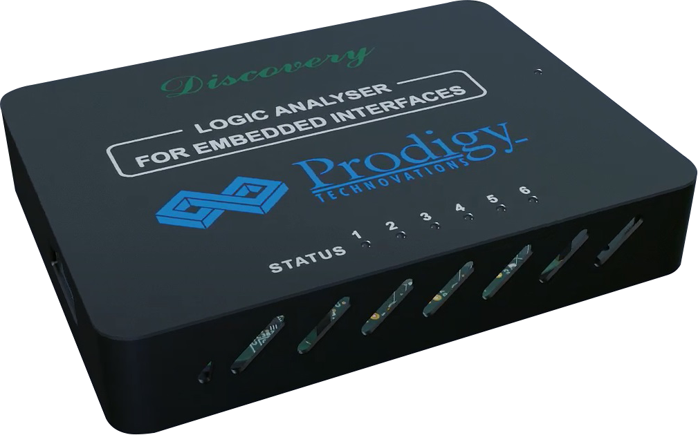
Talking about the build quality, the housing is a complete metal body, giving it an excellent and robust look. The surface has a nice black matte finish along with the company’s branding on the top. The grills at the front and backside help with cooling and adding to the aesthetics of the device. There are four flat rubber legs at the bottom at each corner, which gives it a little elevation and insulation from the working surface. The PGY-LA-EMBD is compact enough to fit in your palm with a dimension of 140 x 100 x 35 mm. Overall, the build quality of all the accessories and the Logic Analyzer feels very durable.

Hardware specifications

PGY-LA-EMBD comes with a 1GS/s (or 1GHz) asynchronous timing speed and 100MS/s synchronous state speed. Discovery series logic analyzers can perform simultaneous protocol analysis of I2C, SPI, UART, I3C, SPMI, and RFFE interfaces on all the 16-channels in embedded system designs. It comes with an input buffer of 4GB DDR3, which is plenty for storing captured data. There are also some advanced trigger capabilities, including auto, pattern, protocol awareness, and timing.

The supported voltage levels are 1.2V, 1.8V, 2.5V, 3.3V, and 5V, selected in the software tool. There are six green LEDs at the top, which indicate the working status, and a PWR LED to indicate the power ON status. An external trigger can be given using the Trigger Out SMA connector on the right side. Additionally, there’s a USB 3.0 port, 5V power port, an ON/OFF switch, and a reset button on the right side. There are two micro-USB ports on the left, a 14-pin connector that is said to be reserved, and a connector for flying lead cable.

Test setup: ESP32 is connected to a BMP280 sensor via I2C

To try out the Logic and Protocol Analyzer modes of PGY-LA-EMBD, I decided to build a setup that would be simple and, at the same time, will operate somewhat at a frequency of 300KHz. My setup consists of an ESP32 DevKit v4 hooked to a BMP280 temperature and pressure sensor via I2C. The ESP32 acts as a master, whereas the sensor acts as a slave. I will try to sniff the Serial Data (SDA) and Serial Clock (SCL) lines while the sensor sends the data.

Prodigy Logic Analyser Hands-on Review Connections

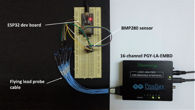
Channel 1 of Logic Analyzer is connected to SDA, and channel two is connected to SCL. The overall setup is quite simple, and everything worked on the first try itself. While this setup doesn’t really do the justice of testing the Logic Analyzer’s high-speed capabilities, it does the job for now.

Software tool

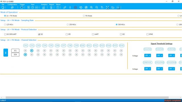
Once the Logic Analyzer is connected to the PC through a USB interface, the software handles the rest of the work of analysis and data representation. The setup is around 14MB which, after installation, takes up to 50MB of disk space. So, it’s lightweight software, which, when opened directly, greets you with the Logic Analyzer setup page. After clicking the “Connect” button, a message displaying “Device connected” pops up, and we’re now ready to capture signals. I selected the Logic and Protocol Analysis mode, a sampling rate of 500MS/s, I2C as the protocol, and finally, channels 1 and 2 as SDA and SCL, respectively.

We need to click the Acquire button with the setup done and the Logic Analyzer will start capturing data. On the Logic Analyzer, LED 1 will now start glowing, indicating that the capture has started. Simultaneously, the software will keep on displaying the acquired data, so you won’t have to wait until the end to get the results. The data will keep on streaming to your PC until you click on the Stop button. LED 1 will be turned off and LED 4 will glow, indicating that capture has stopped.

After capturing the signals, the PGY-LA-EMBD software tool provides a total of three options for viewing – Protocol View, Timing View, and Logic View. Protocol View provides decoded packet information and error information, if any, along with a bus timing view at the bottom. Timing View gives in-depth insights about timing information. Logic View displays the actual state of signals, i.e. High or Low, in a time-correlated format. The interface should be quite familiar if anyone has used a Logic Analyzer before.

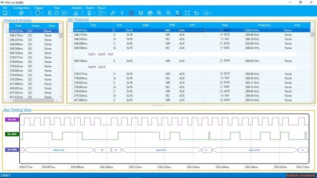
If we look into the table, the 0x76 in the Addr column is the I2C address of the BMP280 sensor. We first wrote a value of 0xF4, requesting the sensor to give out the readings. The sensor acknowledges the ESP32, which can be seen as ACK under the A/N column. After that, the sensor writes out 0x81, 0x68, and 0x0, representing the raw readings coming straight out of the registers in the sensor. Even the waveform at the bottom shows what type and value of data were transmitted at each instance of time.

Final thoughts

To sum up, the whole process of getting started with the PGY-LA-EMBD Logic Analyzer and capturing the data did not take much time; in fact, writing this article took a longer time than this. The labeling on the probe cables helped a lot as normally I would check the connections 3-4 times to make sure nothing is wrong. The software GUI is pretty straightforward and displays all the important stuff on a single page.

While operating, the PGY-LA-EMBD Logic Analyzer does heat up a little bit, and it is more noticeable with the full metal body. However, it is not a major concern as the grills on the front and back dissipates the heat passively. For an end-user, the hefty price tag of $1500 of the PGY-LA-EMBD can be justified with a trove of features. This includes 1GS/s sampling speed, support for I3C, RFFE, and SPMI protocols through a software upgrade in the future (field upgradable), offline decoding capabilities, and also Python API support. So, it can be termed as a future-proof product and seems to be worth investing in.

You can learn more about PGY-LA-EMBD Logic Analyzer on its product page or request a demo before buying one.

Open Source Unsurv Offline Features ESP32, GNSS

A campaign has been launched on Crowd supply for Unsurv, which is an offline privacy-friendly, small, lightweight PCB (43 mm x 32 mm) loaded with an ESP32, GNSS reciever and NFC capabilities. It functions by using a combination of OpenStreetMap data on the SD card, and a custom Android app, enabling you to gather GNSS data throughout the day, and easily analyzing it and using it later on. Speaking about Unsurv, the company says:

“Our goal is to enable a broad discussion about invasive technologies that follow us increasingly closer in our daily lives and to help disrupt familiarization to offline surveillance.”

You can use Unsurv for a variety of other location-tracking functions, and you can access your Unsurv data easily via your smartphone and the dynamic NFC Tag which is fitted into the case. The Unsurv features a tiny BMA400 accelerometer which helps save precious battery capacity by managing power-saving features. It can even be adapted as an input device with tap and double-tap recognition. It is easy to use, just add a single cell LiPo battery, or USB power bank for more demanding tasks, and start gathering data. Unsurv is very efficient because, at the end of the day, most common Global Navigation Satellite System (GNSS) projects appear onto Unsurv offline, inclusive of surveillance cameras you would otherwise not notice.

Unsurv has many uses. It can perform simple location logging, automated commute tracking, and map WiFi signal strength. This enables you to log your daily commute by bike and ensure that no one except you has the data. You can also map WiFi signal strength in your city and create a map of free WiFi access points. Also, if you use vehicles commercially and want to claim tax benefits, you can use Unsurv offline to log each trip. Unsurv offline is open source, so it enables you to come up with your own custom uses.

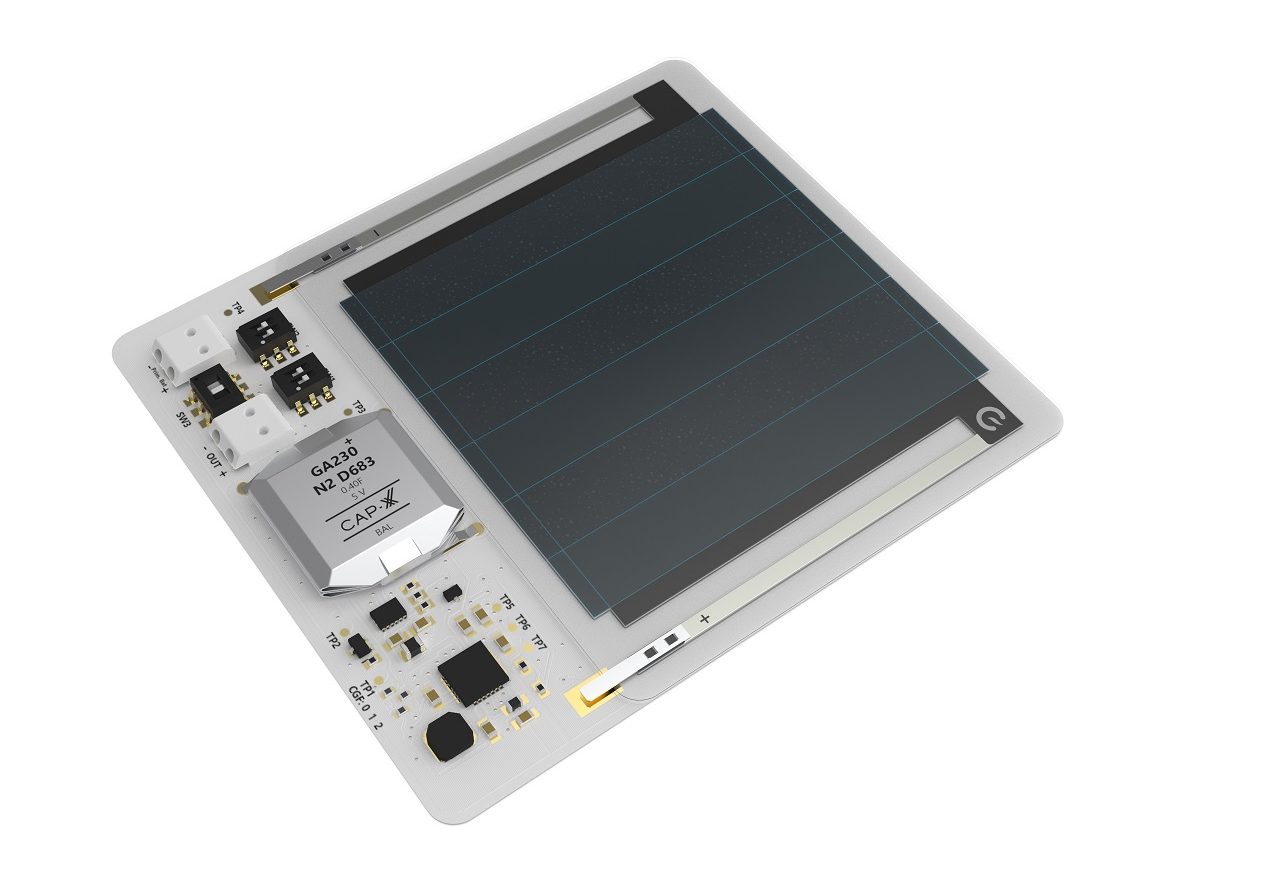
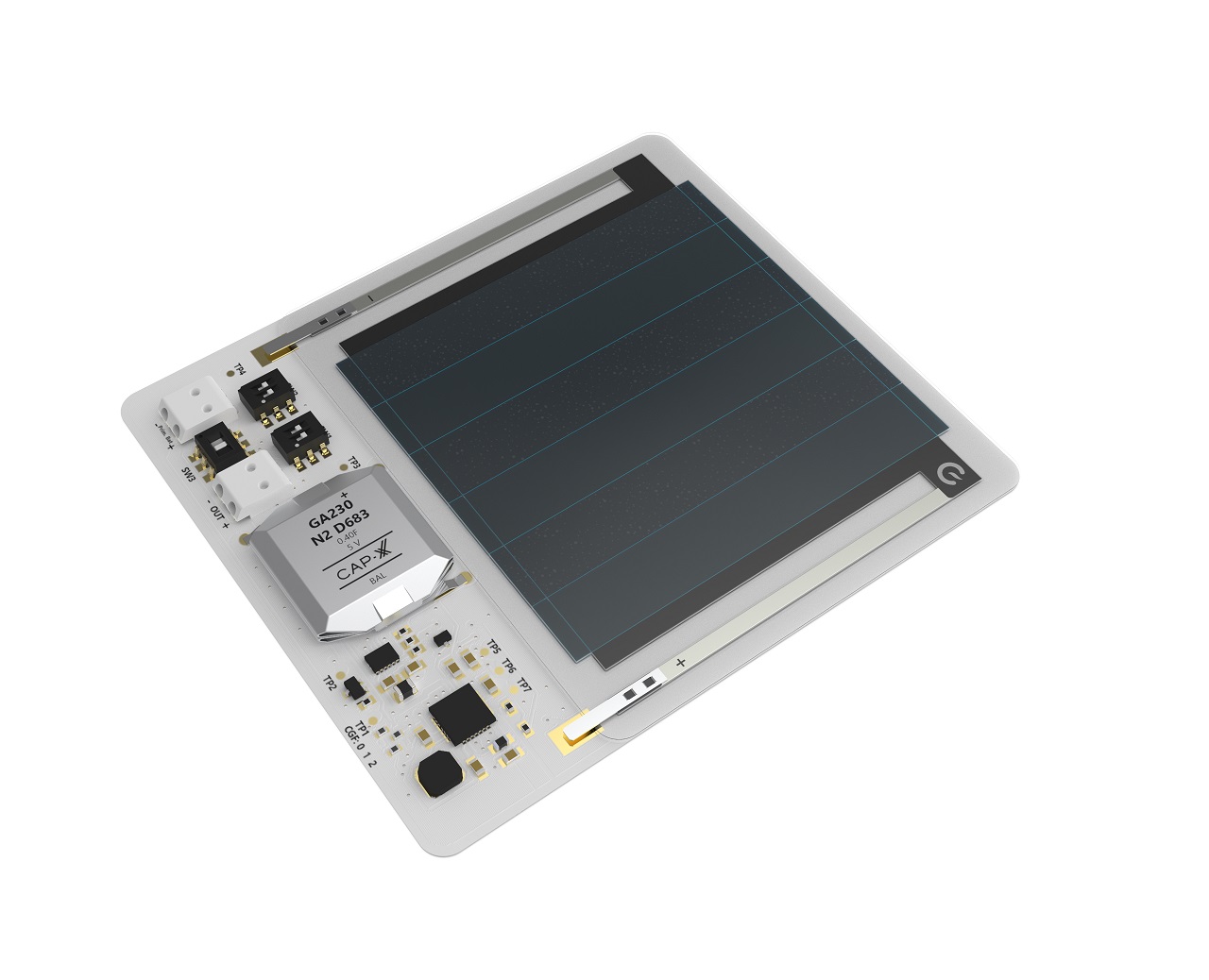
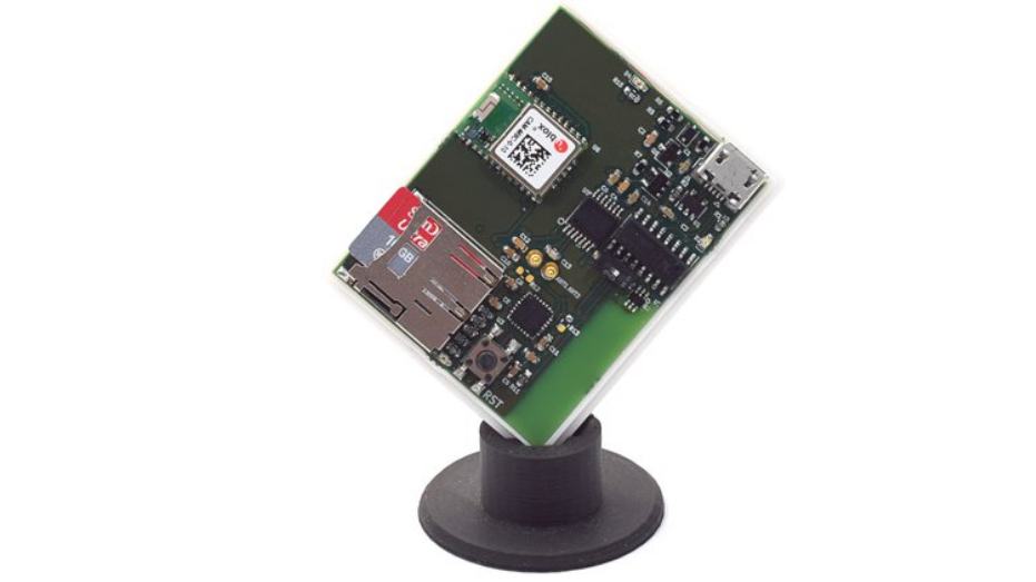
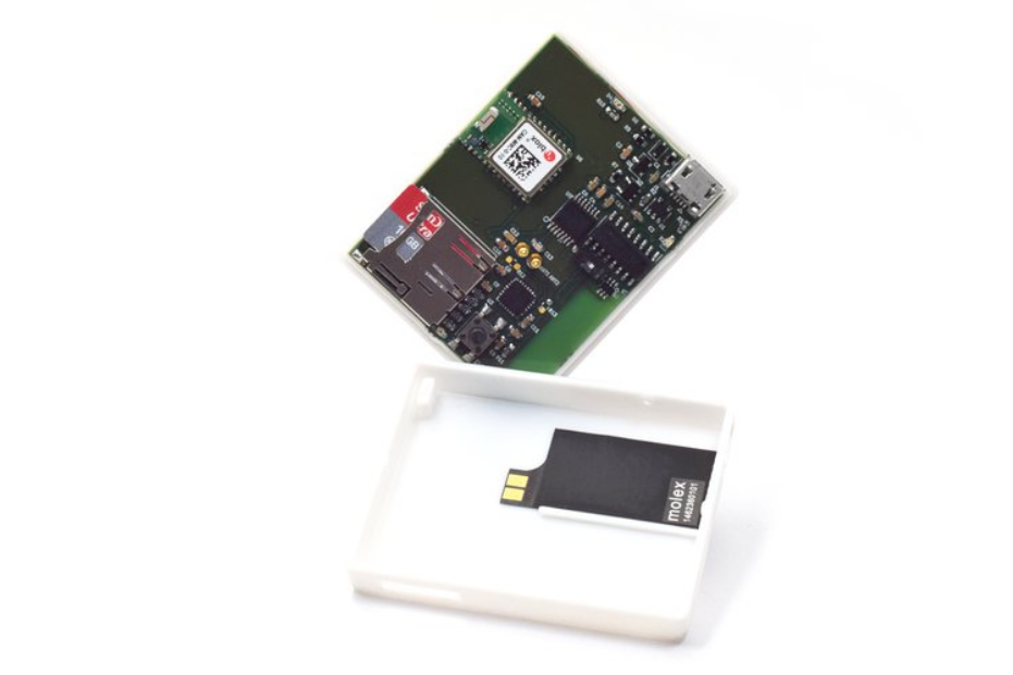
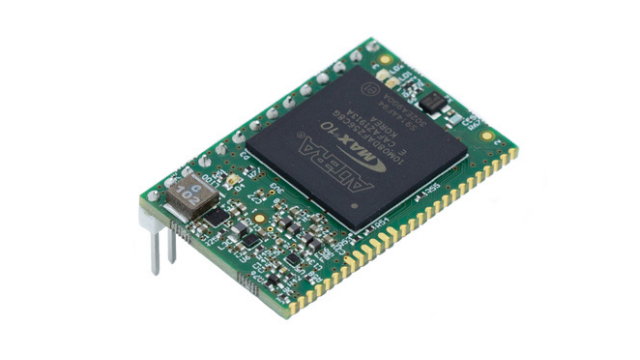
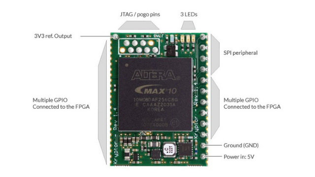
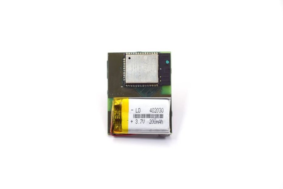
When you use an always-on location service on a smartphone, it increases power consumption and is not sustainable to use throughout the day. It can also expose your location to third parties, thereby taking away from the security focus. However, Unsurv solves all of this problems since it is a custom lightweight, portable, low-power board with every feature you need for powerful location tracking.

Features & Specifications

  • Ublox cam m8c GNSS receiver (GPS, Galileo, GLONASS, BeiDou)
  • ESP32 Pico D4 Microcontroller
  • Texas Instruments RF430CL330 dynamic NFC Interface
  • Bosch BMA400 accelerometer for power-saving features
  • MCP73831 single-cell Li-Ion battery charger
  • Micro SD slot
  • 5 ways to access your data:
    • NFC
    • Bluetooth
    • WiFi
    • SD card
    • micro USB

If you are interested in this device, you can follow the development and have a look at the hardware design on GitHub. The company plans to make the Android app, and firmware for the use case, and also other common use cases publicly available. You can find more information on the campaign page on crowd supply.

Open Source Kryptor FPGA with Dedicated Hardware Security Module

Kryptor FPGA

Kryptor FPGA has been around in the pre-launch phase for over two years. After a significant amount of time and wait, the one-chip hardware security module Kryptor FPGA has launched for crowdfunding on Crowdsupply with the goal of $13,000. This compact FPGA hardware security module brings ease and flexibility for deployment in the IoT space. Kryptor FPGA can become the favorite board for IoT-developer and maker communities looking for multifunctionality of the HSM along with the custom soft-core.

At the heart of the board is the Altera MAX10 FPGA chip that features 55 nm TSMC embedded flash process technology. The FPGA has a four-input look-up table (LUT) and a single register logic element (LE) with a total of 8000 LUT/LE. The flash memory retention is around 20 years at 85°C and speeds up to 830 Mbps.

Parameters to Know About Kryptor FPGA:

  • FPGA: Altera MAX10 FPGA chip
  • Memory: 378 Kb total
  • Storage: 1376 Kb
  • Compatible platforms: Linux, Raspberry Pi (RPi), and Arduino
  • Interface: SPI, UART, I²C
  • GPIOs: 250 available from the FPGA (fewer accessible via the board)
  • Dimensions: 22.8 x 31.2 mm

Kryptor FPGA Specs

One of the most highlighting factors of the hardware is the dedicated hardware security module that is missing in popular hardware like iCEBreaker FPGA, TinyFPGA BX, and NiteFury. With open-source hardware design, it possesses greater reliability and verifiability of encryption techniques. This allows the user to look at the schematics of the design and self-verify the techniques using the open-source encryption primitives and not trust the chip manufacturer for its security.

Kryptor FPGA is compatible with Raspberry Pi API and Arduino library which makes it easy for the users to play with the available APIs for Linux. Once you buy the hardware, the designer SKUDO Kryptor will provide the option to download the HSM soft-core from the official website at no extra cost. With the flexibility in the hardware, the user gets the option of either using it as a MAX10 FPGA development board or can even load their own soft-core.

If you are interested in backing the product and getting perks for it, head to the crowdfunding page and help with this open-source project.

ADA4570 Anisotropic Magnetoresistive (AMR) Sensors

Analog Devices’ integrated AMR angle sensor and signal conditioner with differential outputs

ADI’s ADA4570 is an AMR sensor with integrated signal conditioning amplifiers and ADC drivers. It produces four analog outputs that indicate the angular position of the surrounding magnetic field. The ADA4570 consists of two die within one package, an AMR sensor, and a fixed gain instrumentation amplifier. It delivers clean and amplified differential cosine and sine output signals related to the angle of a rotating magnetic field. The output voltage range is radiometric to the supply voltage.

Features

  • Boost and dual buck synchronous controllers allow all outputs to remain in regulation during automotive restart or cold crank
  • VIN range of 4.5 V to 40 V and operates down to 1 V after startup
  • Low 14 µA operating quiescent current extends the battery run time during a standby condition

more information: https://www.analog.com/en/products/ada4570.html

RT1105 Series Reverse Through-Hole Tact Switch

E-Switch’s RT1105 tact switch features a soft silicon 4.40 mm high actuator and provides multiple gram force options

E-Switch’s RT1105 series reverse through-hole tact switch with multiple gram force options provides up to 100,000 cycle life expectancy in a 6.80 mm x 6.80 mm footprint. This switch series features a soft silicon actuator 4.40 mm high and provides multiple gram force options identified by different color actuators, 160 gf (red), 260 gf (dark gray), and 350 gf (blue). The RT1105 tact series features include SPST-NO, off-(on); 50 mA, 12 VDC contact rating, dielectric strength of 250 VAC for 1 minute; operating temperature ranges from -20°C to +85°C; travel is 0.25 mm, and comes in tray packaging.

This tact series is suitable for audio/visual equipment, computer peripherals, computer electronics, medical equipment, telecommunication devices, and test and instrumentation equipment.

Features

  • Contact rating: 50 mA, 12 VDC
  • Electrical life: 100,000 cycles
  • Dielectric strength: 250 VAC for 1 minute
  • Operating temperature: -20°C to +85°C
  • Operating force: 160 gf (red), 260 gf (dark gray), and 350 gf (blue)
  • Contact arrangement: SPST off-(on)
  • Contact resistance: 100 mΩ max. (initial)
  • Insulation resistance: 100 MΩ at 100 VDC
  • Travel: 0.25 mm
  • Bounce: 10 m sec. max

more information: https://www.digikey.com/catalog/en/partgroup/rt1105-series/81904

Maxim Integrated MAX31827 Low-Power Temperature Switch

Maxim Integrated MAX31827 Low-Power Temperature Switch provides an ±1°C accuracy from -40°C to +125°C (12 bits) local temperature switch and sensor with I2C/SMBus interface. The MAX31827 switch offers high accuracy in a small 6-bump wafer-level package (WLP), making it ideal for a wide range of applications.

The Maxim MAX31827 Low-Power Temperature Switch can be used as a temperature switch with preconfigured thresholds or a temperature sensor with an I2C interface. When the MAX31827 operates as an independent temperature switch, the I2C interface doesn’t have to be used. Without utilizing the I2C interface, the switch can be used in systems that require thermal protection implemented in hardware, without the need for reconfiguration or use of software/firmware during normal operation. Additionally, the one-time programmable (OTP) ALARM functionality enables the use of the MAX31827 as a safety mechanism in systems where power dissipation is challenging.

The I2C/SMBus-compatible serial interface permits standard, write and read commands to read the temperature data and configure the behavior of the sensor. The bus timeout resets the interface if the clock is low for more than 30ms (nominal), and packet error checking (PEC) helps prevent communication errors when used with a master that supports this feature.

The MAX31827 is housed in a 6-bump WLP and operates over a -45°C to +145°C temperature range.

Features

  • Stand-alone temperature switch with preconfigured
  • Alarm thresholds and hysteresis
  • Active high/active low/open drain ALARM output
  • Excellent temperature accuracy
    • Maximum ±1.75°C from -45°C to +145°C
    • Maximum ±1°C from -40°C to +125°C (12 bits)
  • External resistor selects an address for location identification
  • Temperature resolution is selectable from 8 to 12 Bits
  • Selectable timeout prevents bus lockup (default enabled)
  • I2C and SMBus support
  • User-defined alarm settings
  • Selectable PEC for reliable communications
  • Up to 1MHz Bus Speed
  • +1.6V to +3.6V Power supply voltage

Build Your Private Online Parts Warehouse in JLCPCB

Have you ever encountered the situation that when you place an SMT order, the parts you need have not enough stock or no stock at all?

To solve this issue, JLCPCB provides the pre-order parts feature. It provides customers to set their own online parts warehouse, also be called the parts library in JLCPCB. It allows you to order parts that are in shortage in advance and keep them in your private online parts warehouse, therefore you can get enough parts to be assembled anytime when you are in need.

I will give a brief introduction about how to set your private online parts warehouse in JLCPCB.

Step 1. Visit Parts Manager Page

Sign in to your account, enter your personal center by clicking your account name, and visit the Parts Manager page.

The parts you purchased will be listed on the ” My Parts Lib ” page.

Step 2. Parts ordering

By clicking ” Order Parts “, you can order parts from JLCPCB Parts Library.

For parts in the JLCPCB warehouse:

As JLCPCB needs to keep enough basic parts on the feeder, so the Basic Parts only can be pre-ordered, and there has a minimum order quantity. But normally the basic parts have enough stock, you don’t need to pre-order them.

For in-stock extended parts in JLCPCB warehouse, no minimum order quantity is required. You can directly buy those in-stock parts and after you finished the purchase,the parts will show in you online private parts warehouse. You do need to worry about the shortage when you need it.

For non-stock extended parts in JLCPCB warehouse, you need to pre-order them, and there has a minimum order quantity.

For parts in the LCSC warehouse:

All parts have a minimum order quantity and must be ordered in multiples. LCSC parts’ price is estimated. JLCPCB will purchase parts you ordered from LCSC, then LCSC will ship them to JLCPCB warehouse.

Step 3. Parts Selection

Fill in the quantity you need; click the “Add to My Part Lib” button. The part will be added to the cart.

Step 4. Cart Page Checking

Step 5. Email confirmation

On the ” Checkout ” page, fill in your contact email address. JLCPCB will send the order status to your registered email address by default.

Step 6. Submit Order 

This ordering process is quite simple and it provides many conveniences for customers in the circumstance that parts shortages globally but please note that those parts are only used for your SMT orders you placed on JLCPCB, and they can not be shipped separately.

Step 7. Make payment.

Please complete the payment within one hour, or the order will be canceled automatically because the parts’ inventory may change each second.

Step 8. Order Status Checking

For in-stock items, the parts will usually be shown in your own library immediately after you make the payment.

For the pre-order items, the exact price will be confirmed within 48 hours after the initial payment is done. Money will be refunded or will need to be refilled, depending on the final quotation.

If you don’t want to place SMT orders at JLCPCB, build your private parts warehouse may not be a good idea, because inventory cost and pickup service fee are charged when you need to pick up the components, and it is quite high.

Now JLCPCB has a special offer for SMT orders, no setup fee, and will have a $24 SMT coupon monthly, register now to get a special offer  jlcpcb.com/CPA

Geniatech DB10 AI Development Board For Smart Applications

DB10 AI Development Board

We recently saw a Banana Pi BMP-M2S single-board computer that was powered by the powerful Amlogic A311D processor. Prior to the release of Banana Pi BMP-M2S, the Geniatech DB10 AI development board came to light with the same AI processor onboard. The DB10 AI development board is huge hardware when compared to the Banana Pi BMP-M2S SBC. But of course, looking at the number of interfaces it is justifiable.

Regarding the onboard powerful AI processor featuring quad-core ARM Cortex-A73 and a dual-core Cortex-A53 core with L2 cache to improve system performance. The integrated ARM Mali-G52 MP4 (6EE) supports OpenGL ES 3.2, Vulkan 1.0, and OpenCL 2.0. The hardcore NPU is capable of providing high performance for AI tasks with a speed of 5 TOPS and supports INT8 inference for all deep learning frameworks including TensorFlow and Caffe.

What’s inside Geniatech DB10 AI development board

  • CPU: Quad-core ARM Cortex-A73 and Dual-core ARM Cortex-A53 CPU
  • GPU: ARM Mali-G52 MP4 (6EE)
  • NPU: Performance at 5 TOPS
  • Wireless connectivity: 3G/4G (optional), IEEE 802.11 a/b/g/n/ac, Bluetooth 4.2/5.0(Optional)
  • Memory: 2GB LPDDR4(4GB optional)
  • Storage: 16GB eMM(8~64GB optional)
  • Video interfaces: 1x HDMI IN, 1x HDMI Out,
  • USB: 1x USB3.0, 3x USB2.0,
  • Serial ports: 1x 2-wire UART, 1x 2-wire UART/Debug,
  • Camera interface: 2x MIPI CSI (1 x 4-lane MIPI CSI, 1x 2-lane MIPI CSI),
  • Storage expansion: 1x PCIe,
  • Miscellaneous: 1x speaker, 1x mic
  • OS: Android 11.0 or Linux
  • Power: DC 12V/2A
  • Dimensions: 142mm x 117mm

DB10 AI Development Board Interfaces

The video interface through HDMI IN gives the maximum resolution of up to 1920 x 1080 pixels at 60 frames per second, while the HDMI OUT has the support for maximum resolution of 4096 x 2160 pixels at 60 fps. With the 4GB LPDDR4 variant, the hardware is expected to be smooth for high-end multimedia applications that involve video interfacing.

Geniatech DB10 AI development board comes with optional 3G/4G support while inbuilt Wi-Fi 802.11 a/b/g/n/ac and Bluetooth. It is fascinating to see Wi-Fi 802.11ac support that can give a high data rate for video transfer. The board can be powered using a DC jack at 12V/2A. If you are interested in purchasing the board that runs Android and Linux, please visit the product page where the pricing is not yet disclosed.

TOP PCB Companies