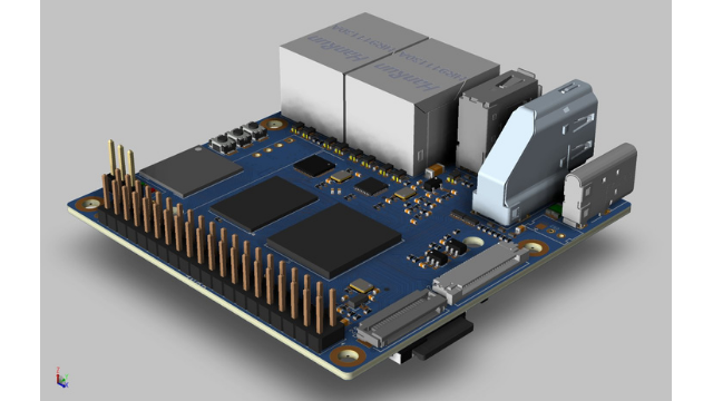
There have been a few single board computers hitting the market that are built around the powerful Amlogic A311D processor. Recently Geniatech released the DB10 AI development board that also came with the same hardcore processor. You can read the article on the DB10 AI development board on the attached link. However, coming back to Banana PiBMP-M2S single board computer featuring the Quad-core ARM Cortex-A73 and Dual-core ARM Cortex-A53 CPU.
When we look at the heart of the single-board computer, the Amlogic A311D processor is an advanced AI application processor designed for hybrid OTT or IP Set-Top Box (STB) and high-end media box applications. The SoC has an integrated CPU, GPU, and neural network accelerator, along with a 4K video CODEC engine. For multimedia applications, the SoC gets HDR image processing with all peripherals, making it a high-performance AI multimedia access point.
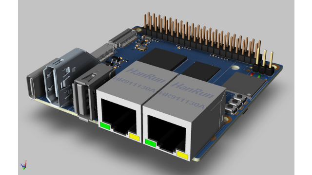
A closer look at Banana Pi BMP-M2S SBC
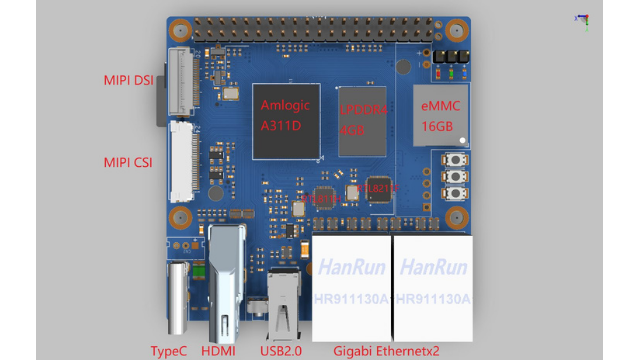
CPU: Quad-core ARM Cortex-A73 and Dual-core ARM Cortex-A53
GPU: ARM G52 MP4(6EE)
Neural Network Accelerator: INT8 inference up to 1536 MAC, supports all major deep learning frameworks including TensorFlow and Caffe
Memory: 4GB LPDDR4
Storage: 16GB eMMC flash and MicroSD card
Interfaces: MIPI CSI, MIPI DSI and HDMI 2.1
GPIOs: 40 Pins
OS: Android and Linux system
Power: USB Type-C port, or via Pin header
Dimensions: 65 x 65mm
The neural processing unit is capable of performing at 5.0 TOPS for deep-neural-network applications. It also comes with the support of all the major deep learning frameworks that help the user deploy several models for their high-end multimedia applications. Integrated with HDMI 2.1, you can stream videos with the processing memory of 4GB LPDDR4. There is also a MIPI CSI and MIPI DSI interface to connect the camera and display to the single-board computer.
When you start playing the hardware, you need to note that the SBC supports Android and Linux OS. For most of the multimedia-designed boards, it is not surprising to see Android support as this board. The board can be powered either using a USB Type-C port or via the pin headers. The board is currently being sent to developers and there is no information on pricing or availability in the public domain yet. According to the CNX-Software, the board is expected to be available in sometime 2022.
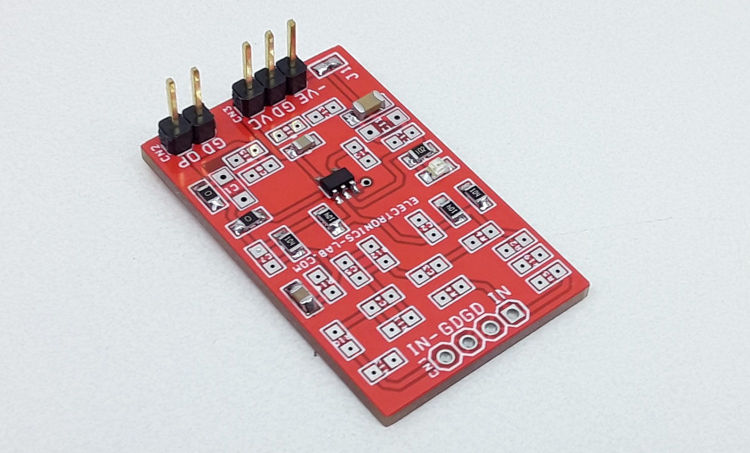
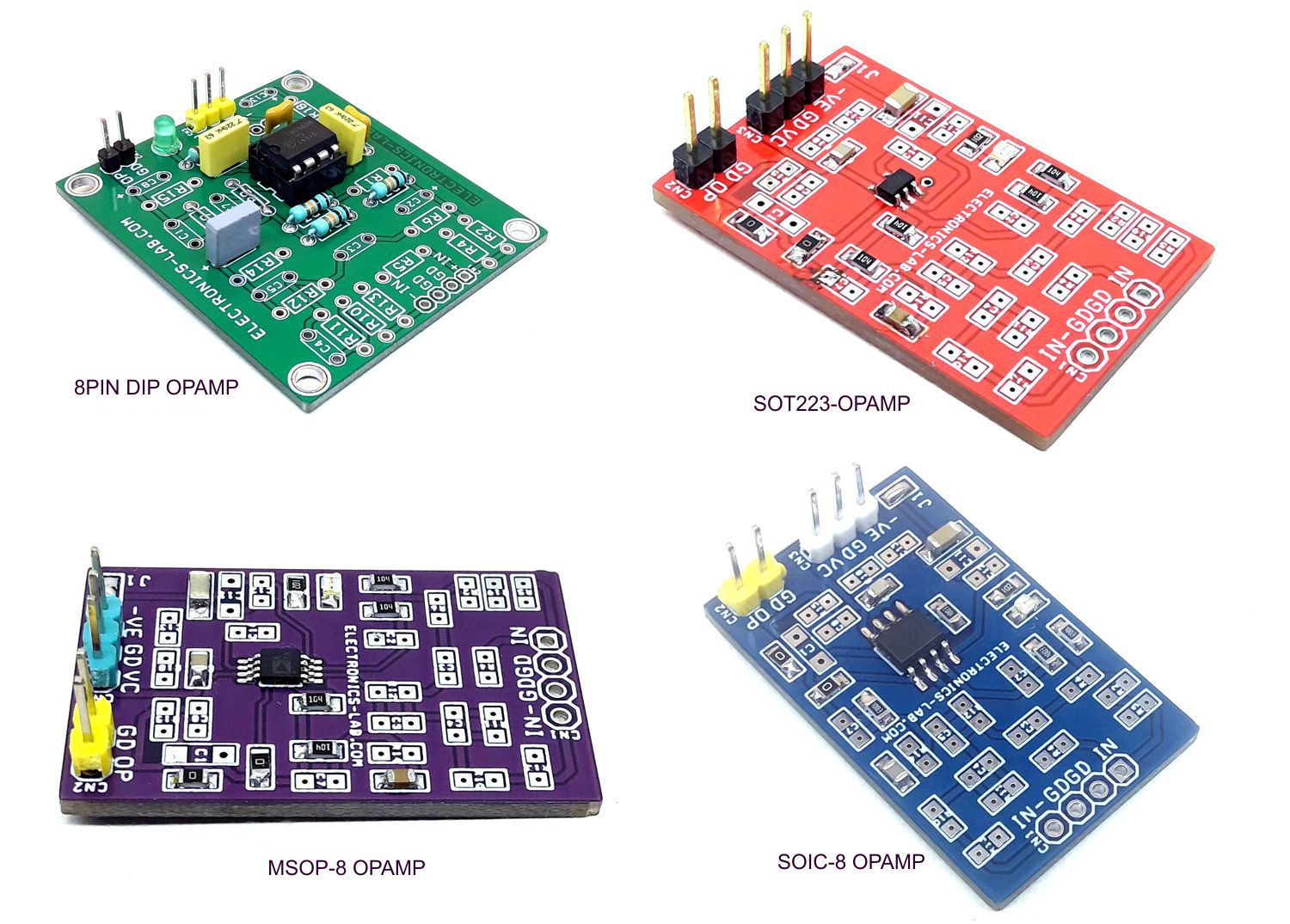
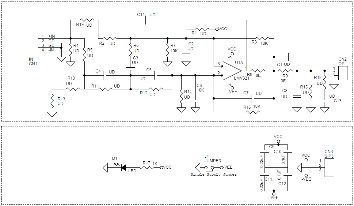
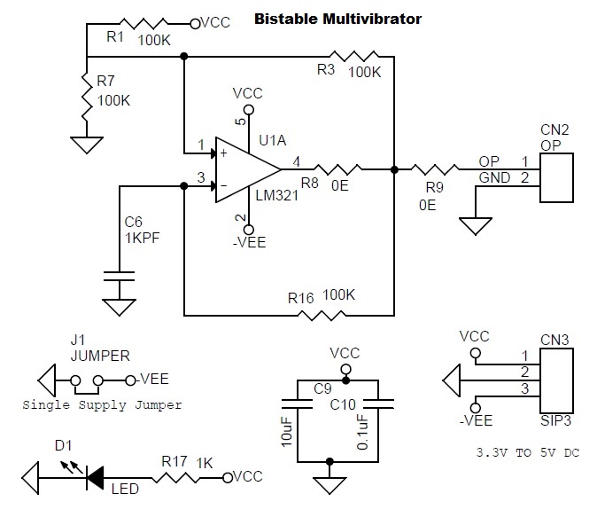
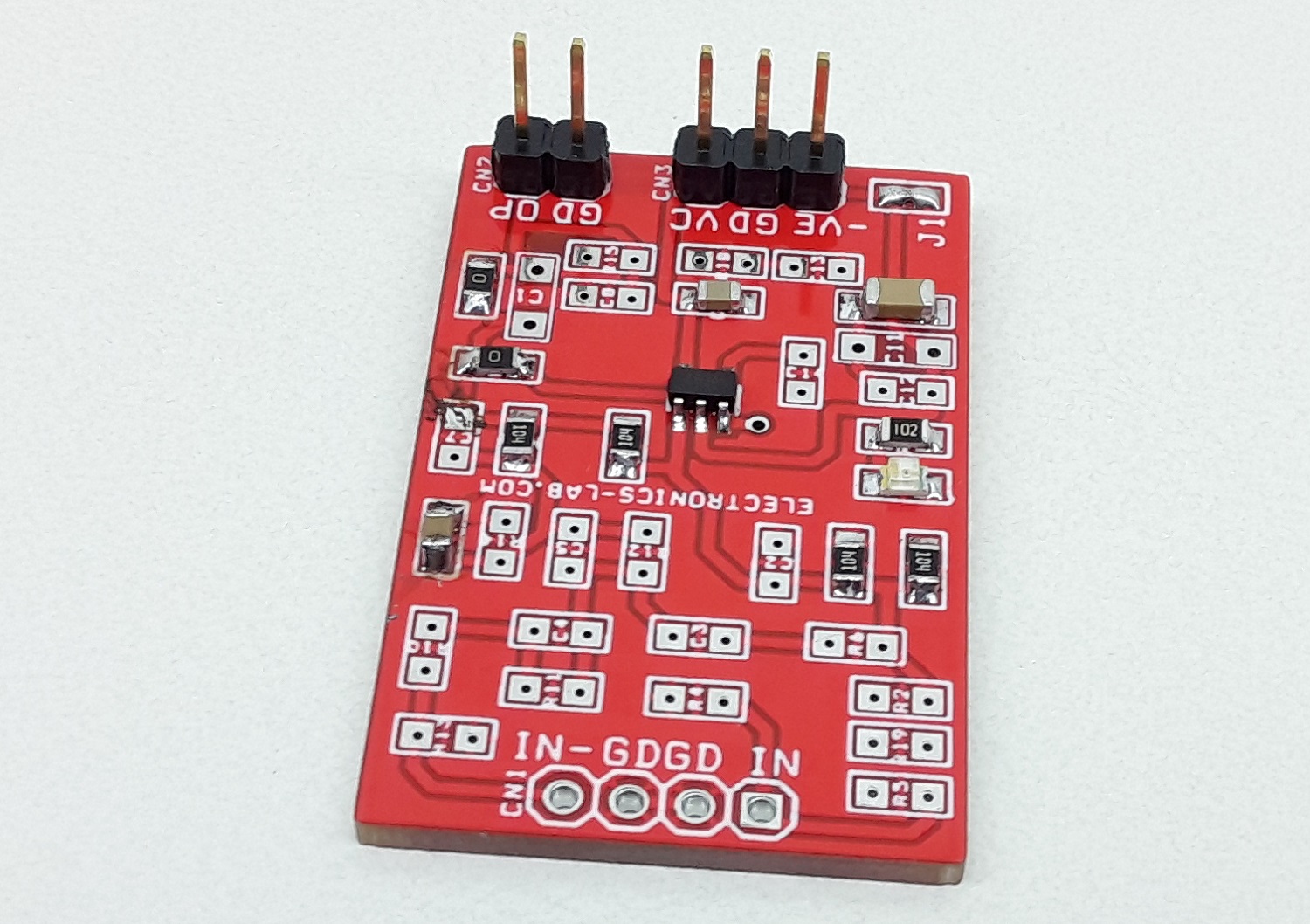
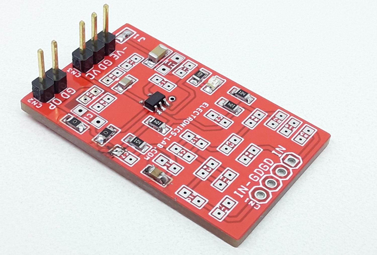
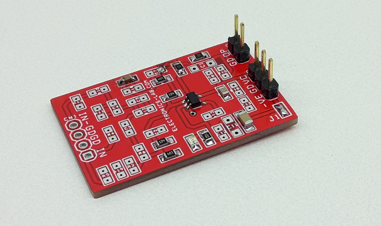
This is easy to build and very useful project for hobbyists and students to learn and create OPAMP-based projects. The project accommodates a single OPAMP in the SOT23-5 package. The project provides the user with multiple choices and extensive flexibility for different applications circuits and configurations. It provides the user with many combinations for various circuit types including active filters, differential amplifiers, and external frequency compensation circuits etc. A few examples of application circuits are given below. LM321 op-amp is the right choice to use for this board or any SOT23-5 OPAMP with the same pin configuration as LM321 can be used. It supports dual supply or single supply, Jumper J1 is provided to use this board with a single supply, D1 power LED.
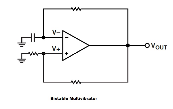
Note: Refer to example circuit to test the board, it is a bistable multivibrator, with single supply Jumper J1 closed.
Credits: All example schematics are from Analog Devices application notes.
Features
Single or Dual Supply User-defined (Jumper)
4 Pin Male Header Connector for inputs
3 Pin Male Header for Supply input (Single or Dual)
Jumper J1 Close for single Supply, Open for Dual Supply
LED D1 Power LED
Any SOT23-5 Op-Amp Can be used Pin configuration – LM321
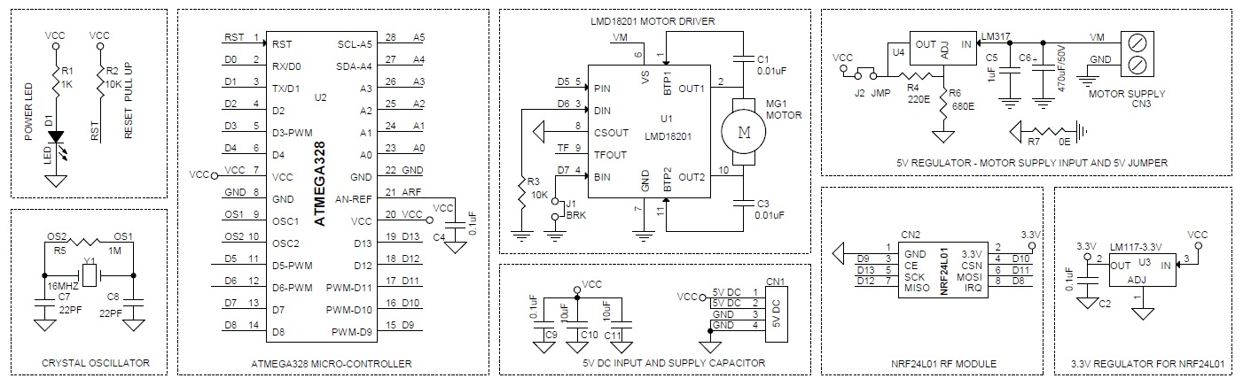
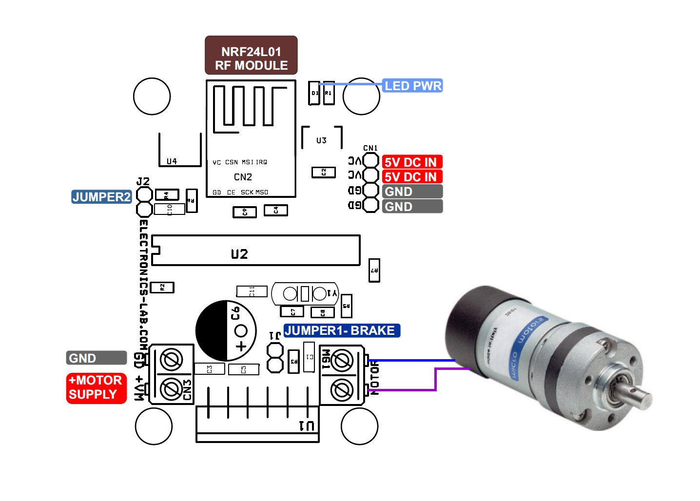
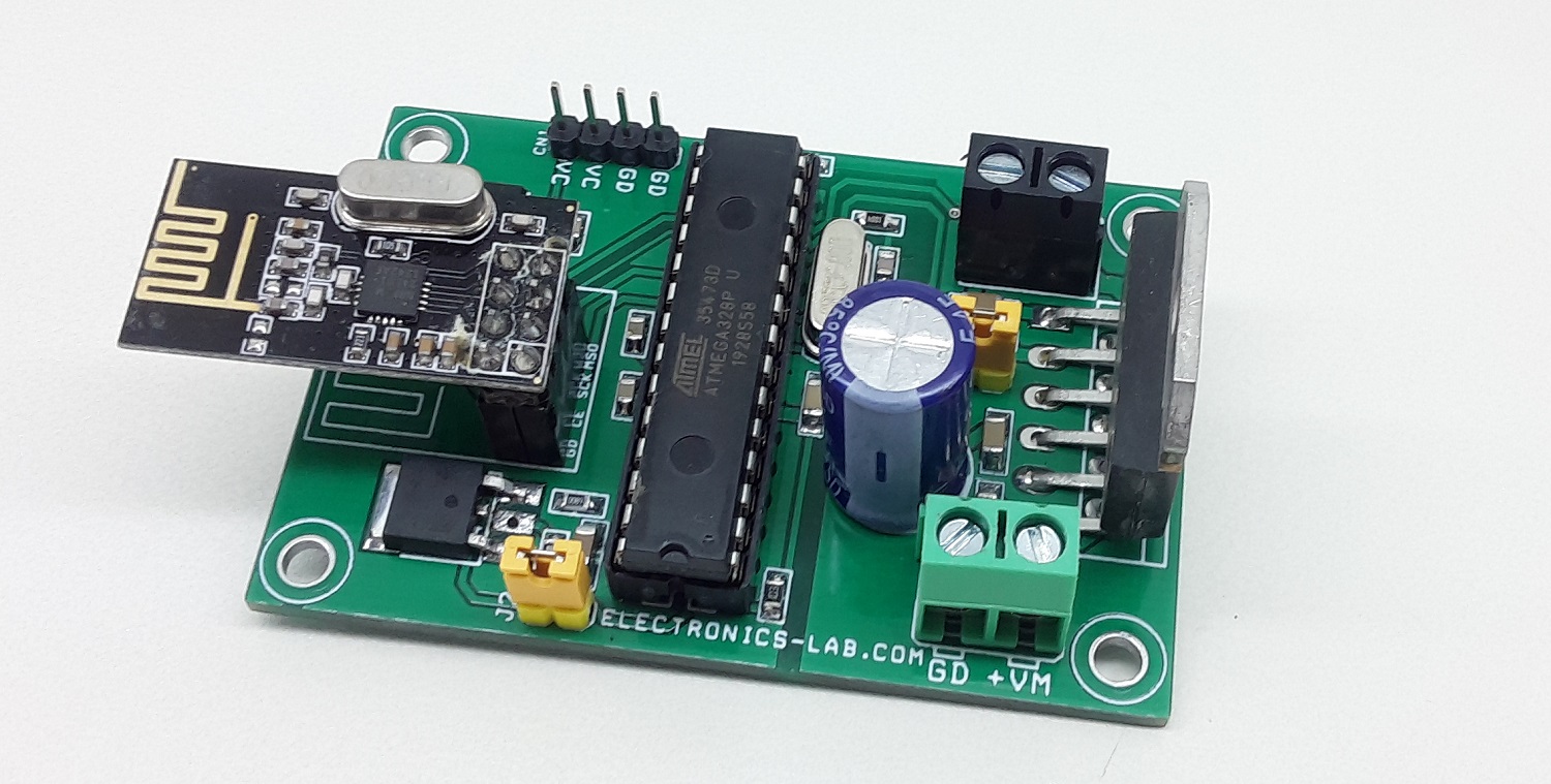
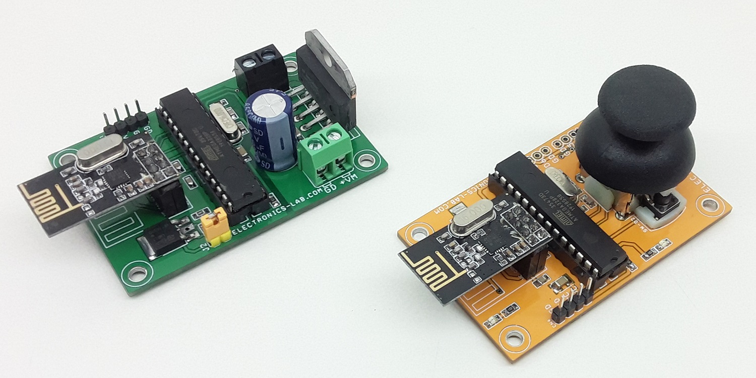
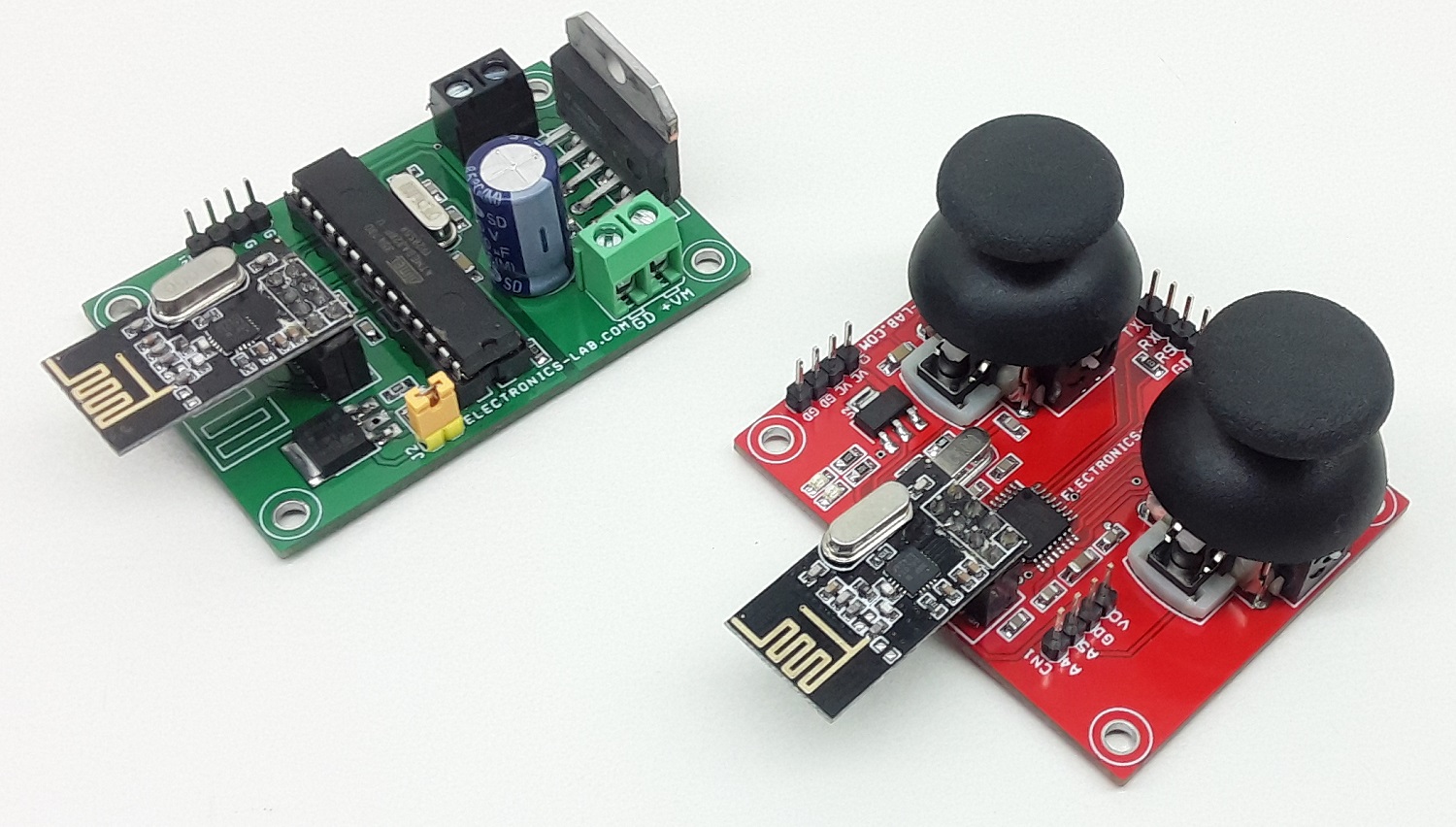
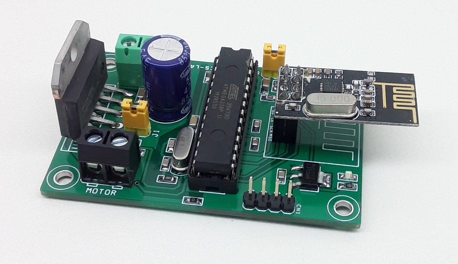
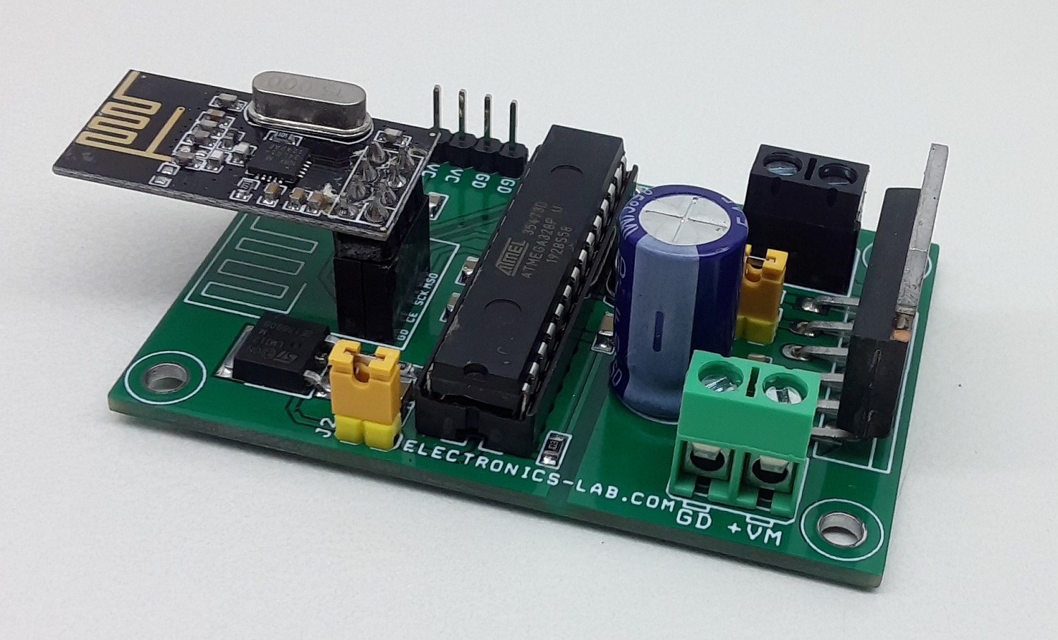
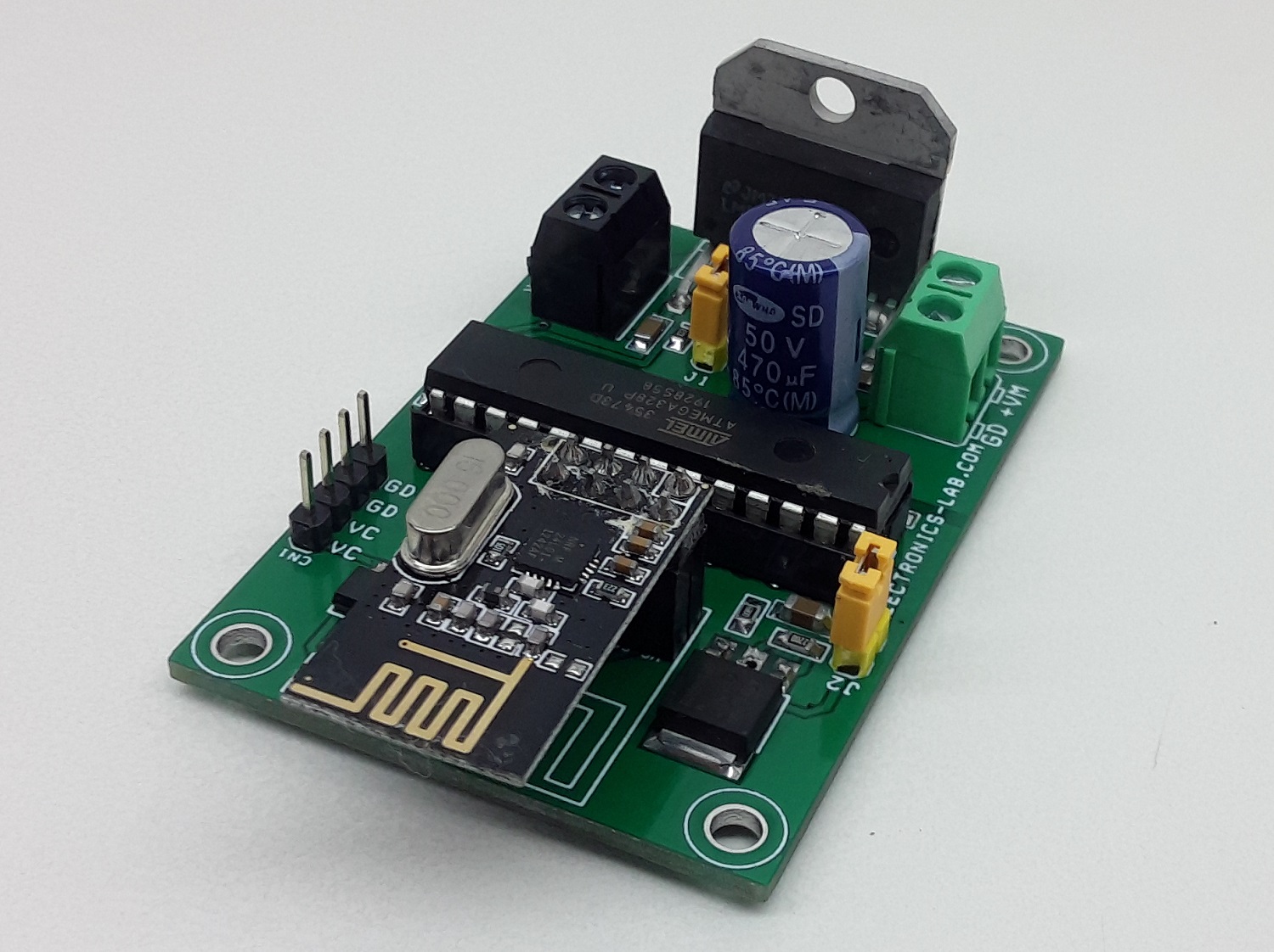
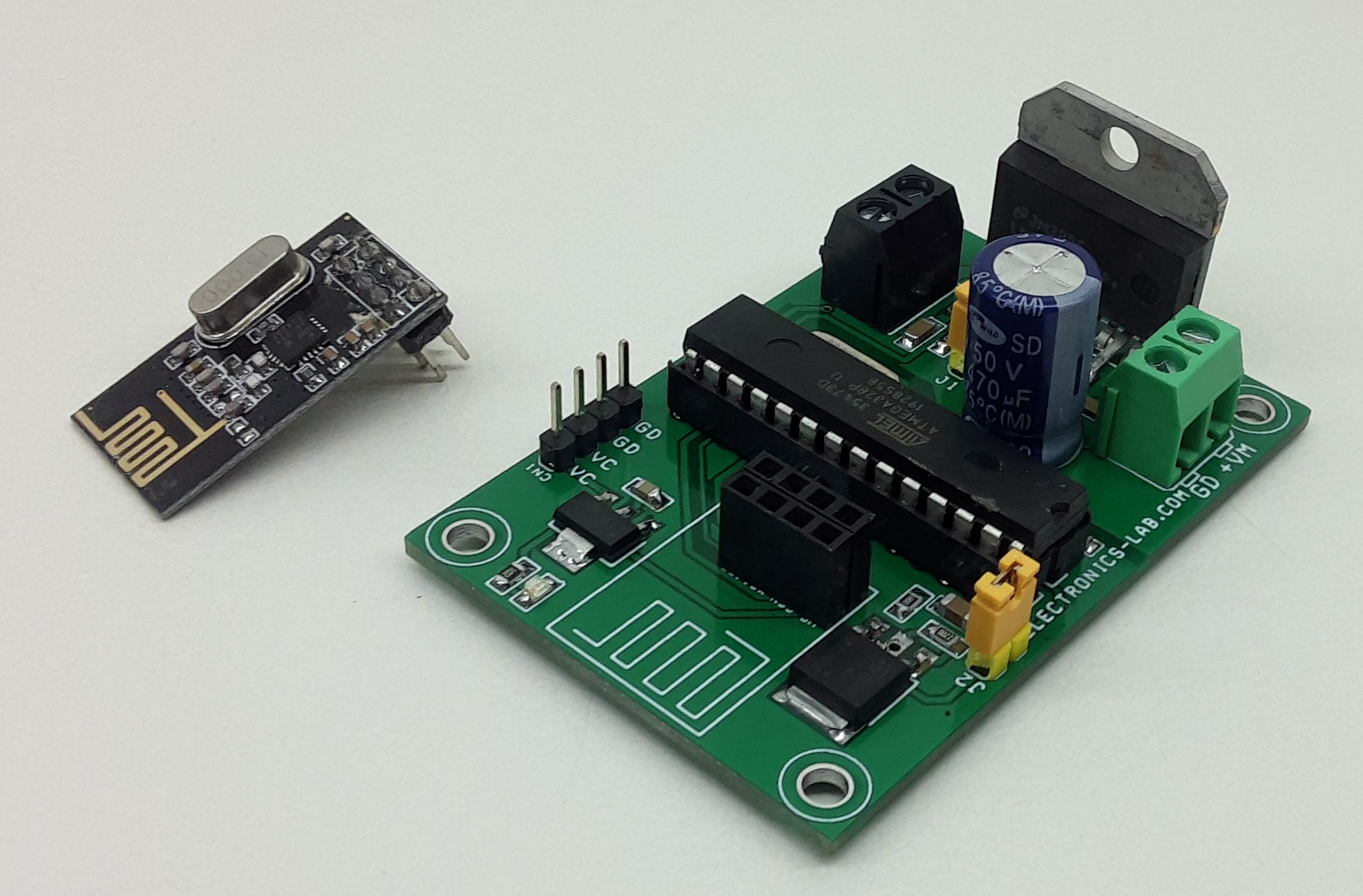
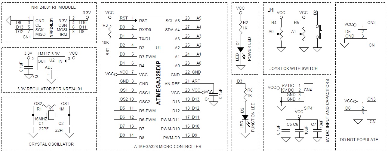
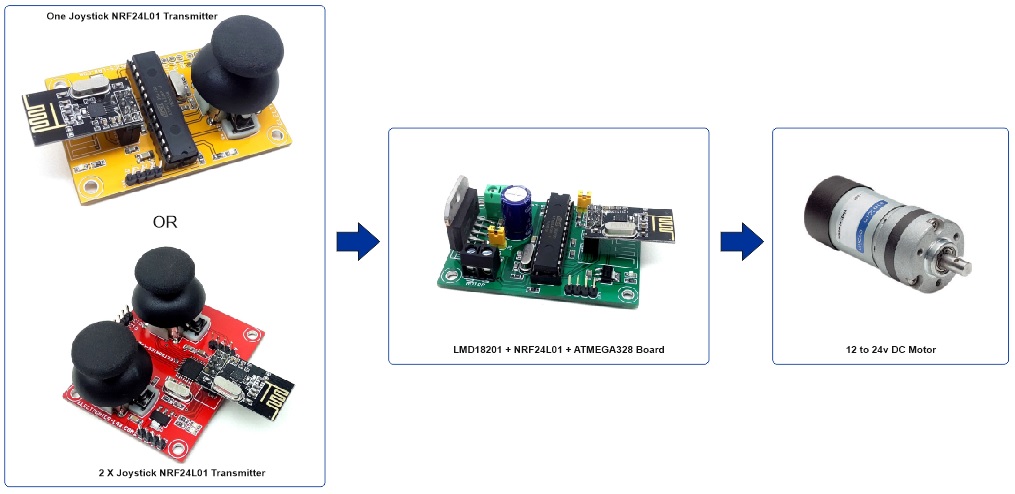
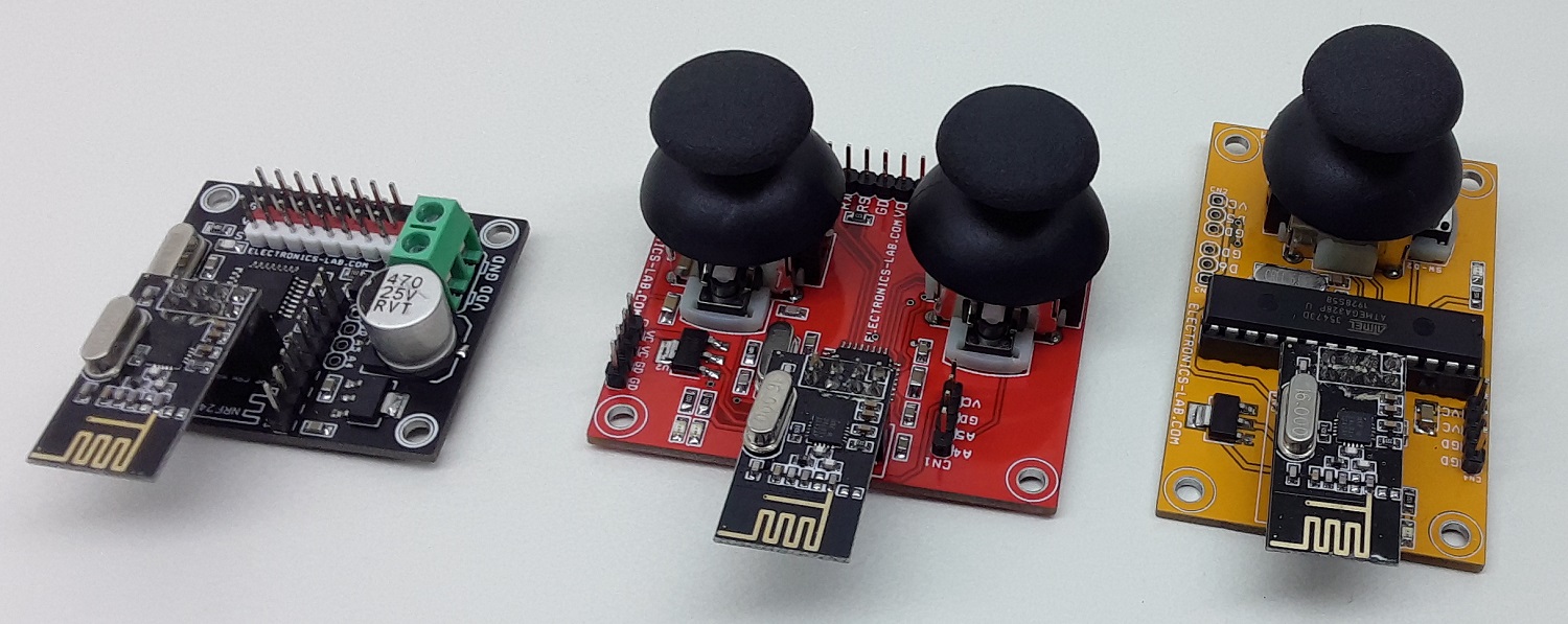
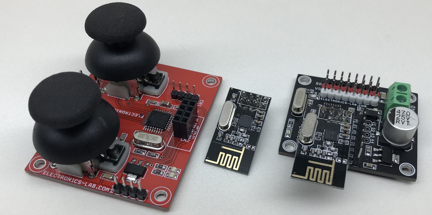
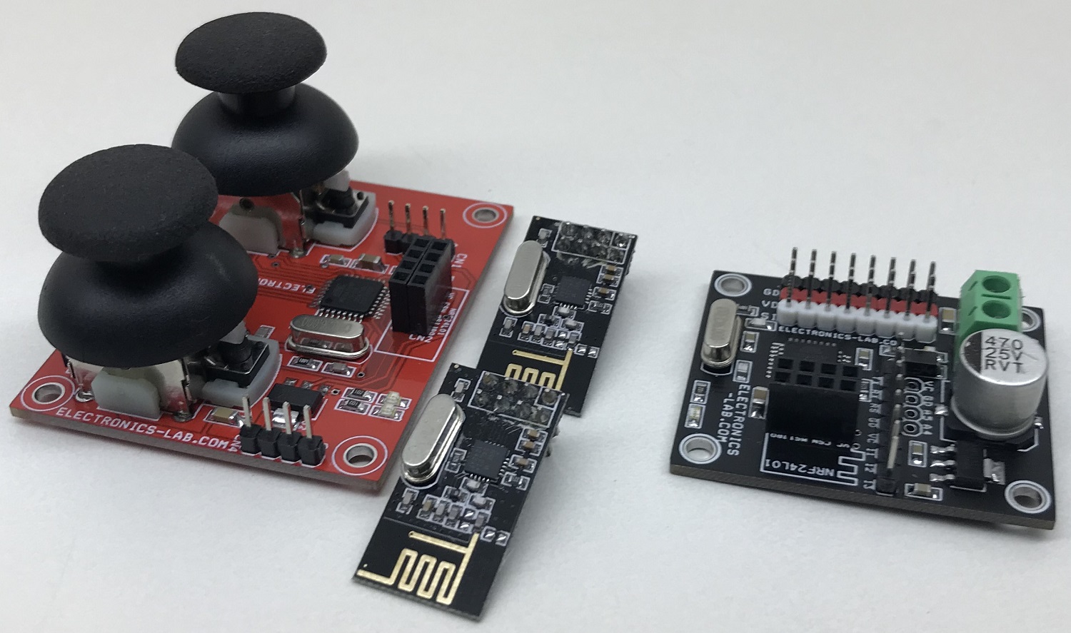
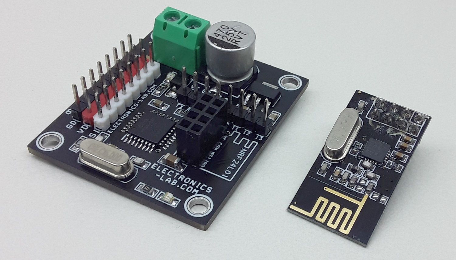
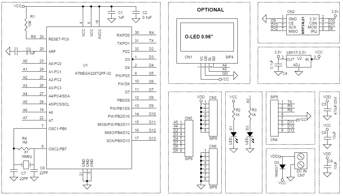
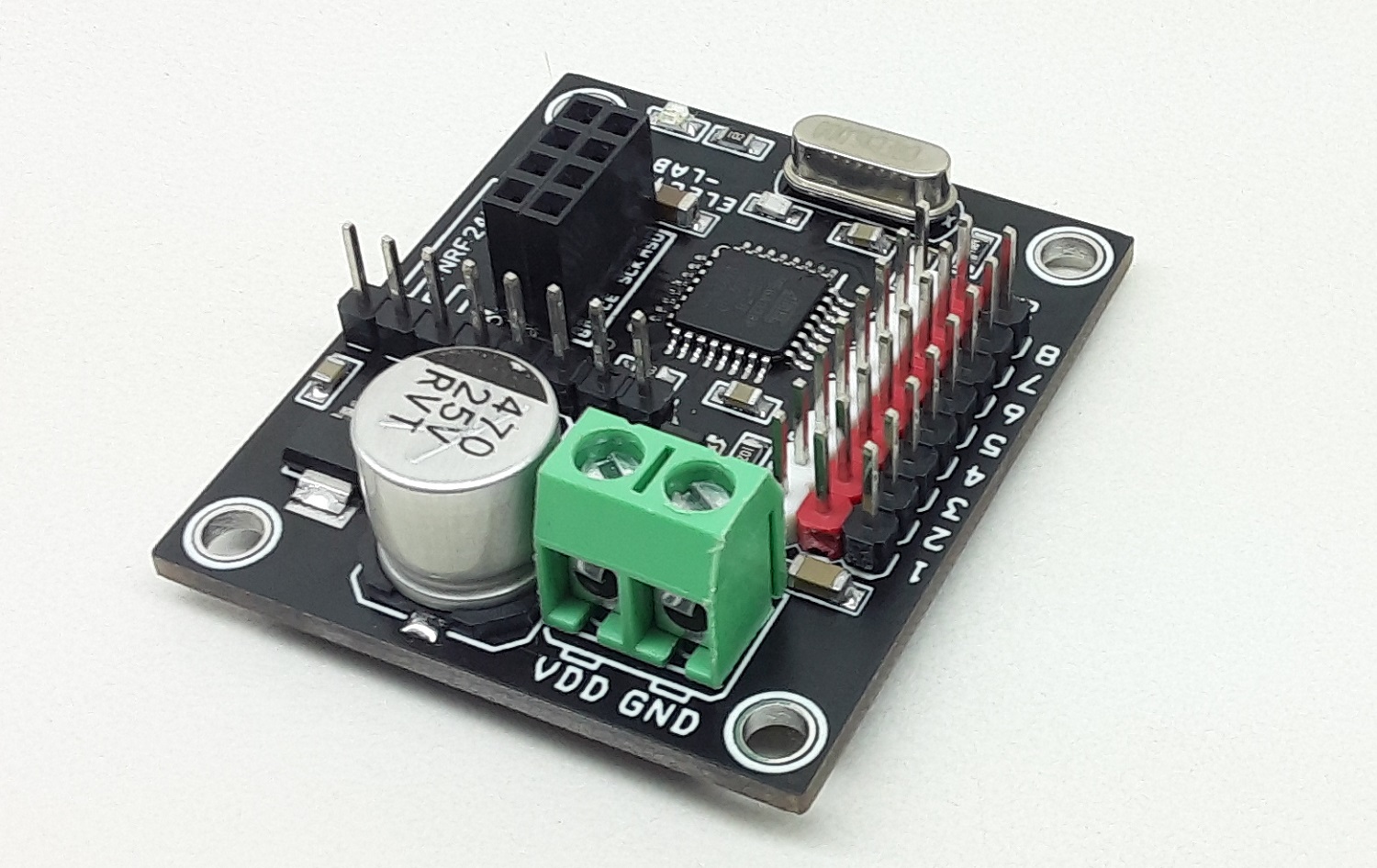
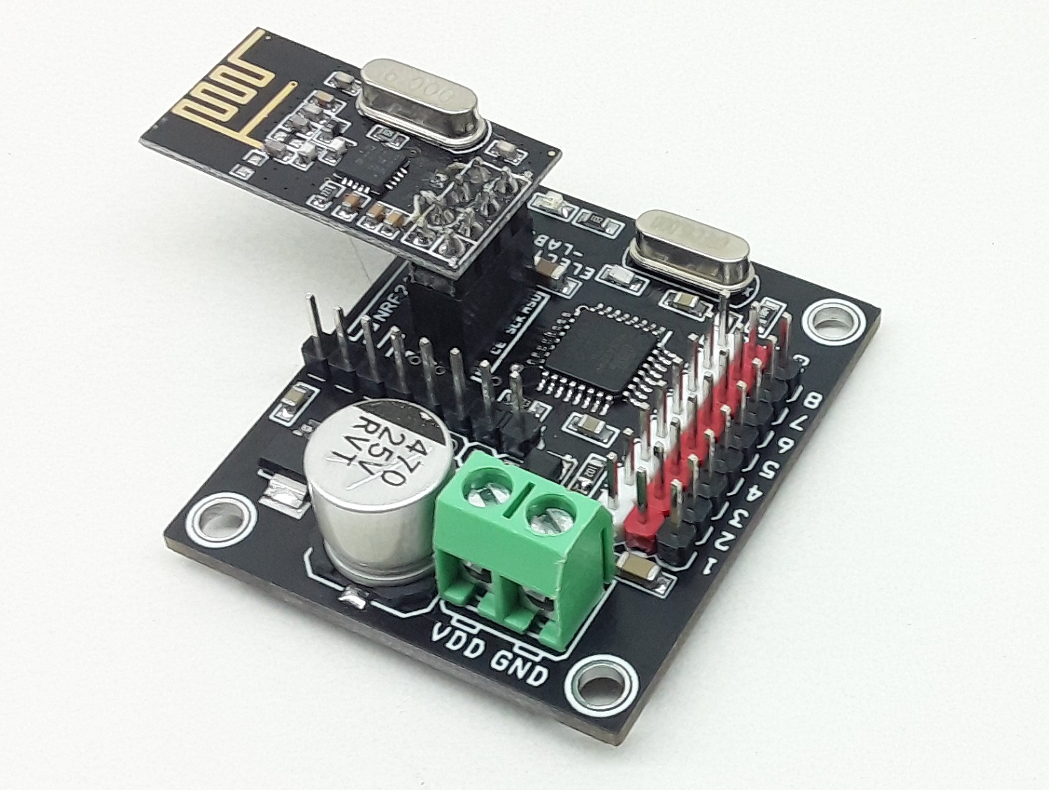
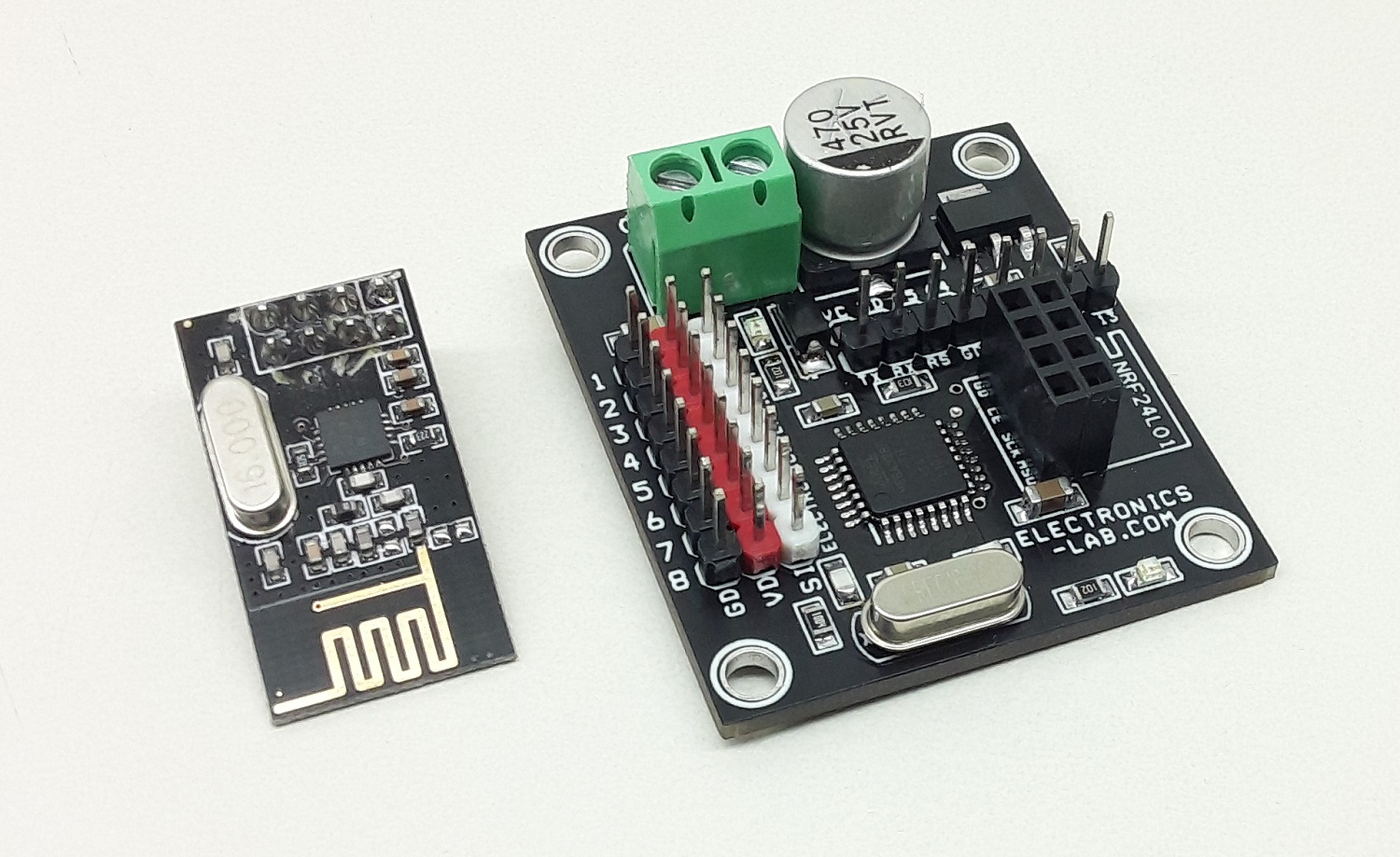
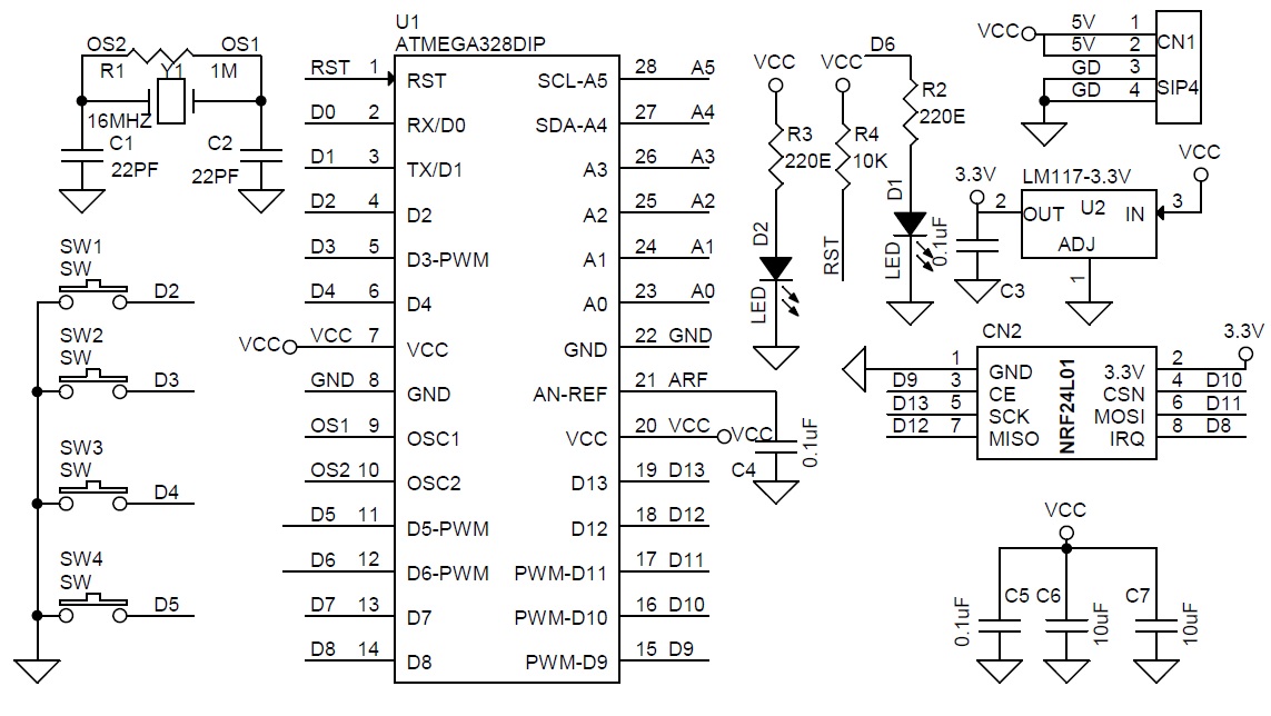
This is Arduino compatible hardware that can control a single DC motor speed, direction, and brake using an RF remote control. The project is based on an ATMEGA328 microcontroller, H-Bridge DC motor driver chip LM18201, NRF24L01 RF module, 5V Regulator, 3.3V regulator and other components. This board can drive a DC Motor up to 24V DC with a load current up to 3A. Arduino pin configuration details are provided below, the user may write their own code and use this hardware. The ATMEGA328 is the heart of the project, the LMD18201 chip drives the motor, LM317-ADJ provides 5V to the microcontroller, LM1117 3.3V regulator power the 3.3V to NRF24L01.
Note 2: The project drives 12V to 24V DC motor with single supply 12V to 24V, LMD18201 can support higher voltage motor up to 48V, in case of 48V supply, remove VCC Jumper J2, apply 48V to CN3 for motor and apply 5V DC separately to CN1 for the microcontroller power.
Note 3: It is advisable to use large size of heatsink on LMD18201 chip.
Note 4: Close Jumper J1 and J2 for normal operations of 12V to 24V DC Motor Speed and Direction Control using Joystick remote transmitter.
Arduino Pins
LMD18201 Motor Driver Chip: PWM-Pin5>> Arduino Digital Pin D5, Direction-Pin3>>Arduino Digital Pin D6, Brake-Pin4>> Arduino Digital Pin 7
NRF24L01 RF Module: GND>>GND, 3.3V>>3.3V Regulator, CE>> Arduino Digital Pin D9, CSN>> Arduino Digital Pin D10, MOSI>>Arduino Digital Pin D11, MISO>> Arduino Digital Pin D12, CSK>>Arduino Digital Pin D13
Code
Arduino code is available as a download, it is a modified code from the original author www.forbiddenbit.com. Make sure RX code is uploaded to the ATMEGA328 chip, TX code is for transmitter chip, follow the link below to learn more about programming and bootloader burning to the ATMEGA328 microcontroller. Users will be able to run DC motor with speed and direction with help of our One Joystick NRF24L01 Transmitter or Dual Joystick Remote over NRF24L01 RF link.
Connect the 12V to 24V DC Motor to MG1 (Motor connector), connect 12V To 24V power supply to CN3, Close Jumper J2 and Jumper J1, Switch on the power, switch on the ON Joystick NRF24L01 Transmitter, the motor should run with Joystick.
Features
Operating Power Supply 12V to 24V DC (Also supports Higher Voltages Read Note 2)
DC Motor Load up to 3Amps
LMD18201 Supports PWM Duty Cycle 0 to 100%
LMD18201 Chip Supports Frequency up to 20Khz (With Example Code Frequency 900Hz)
Motor Speed, Direction, Brake control using RF Transmitter
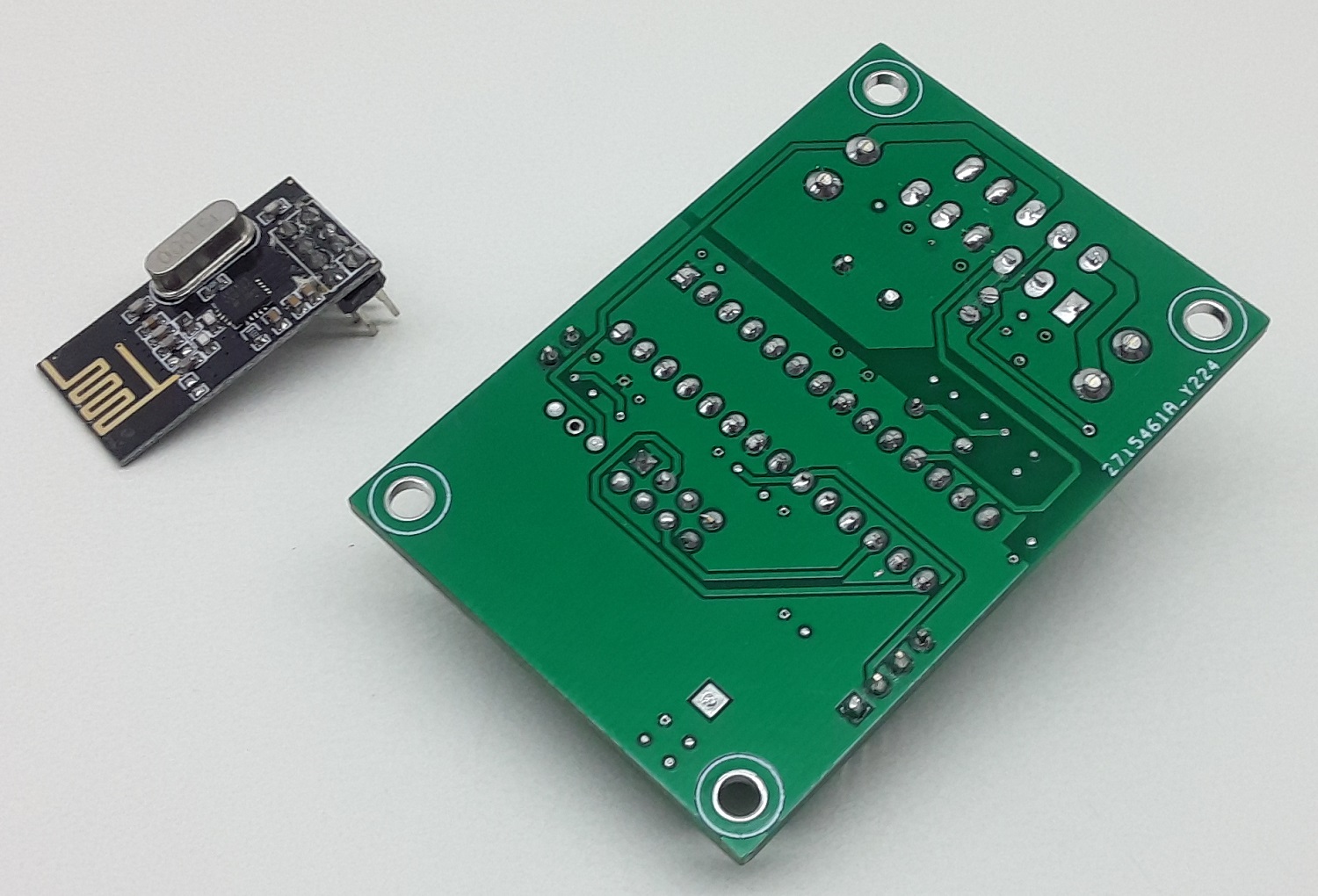
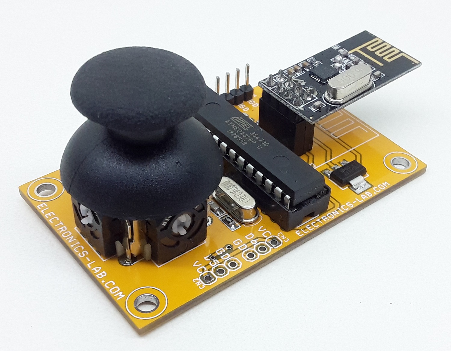
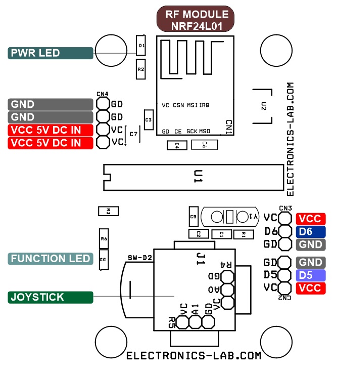
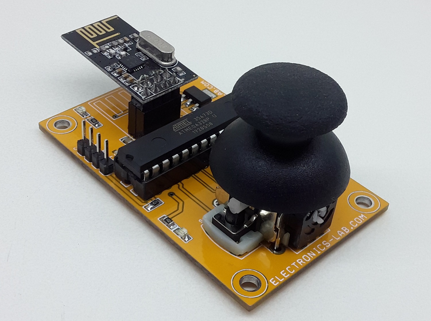
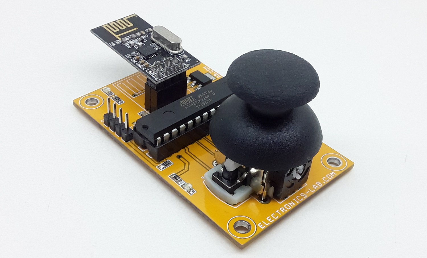
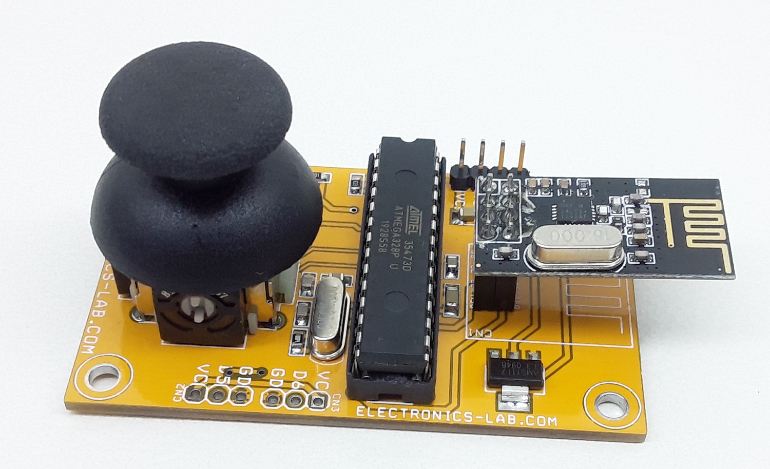
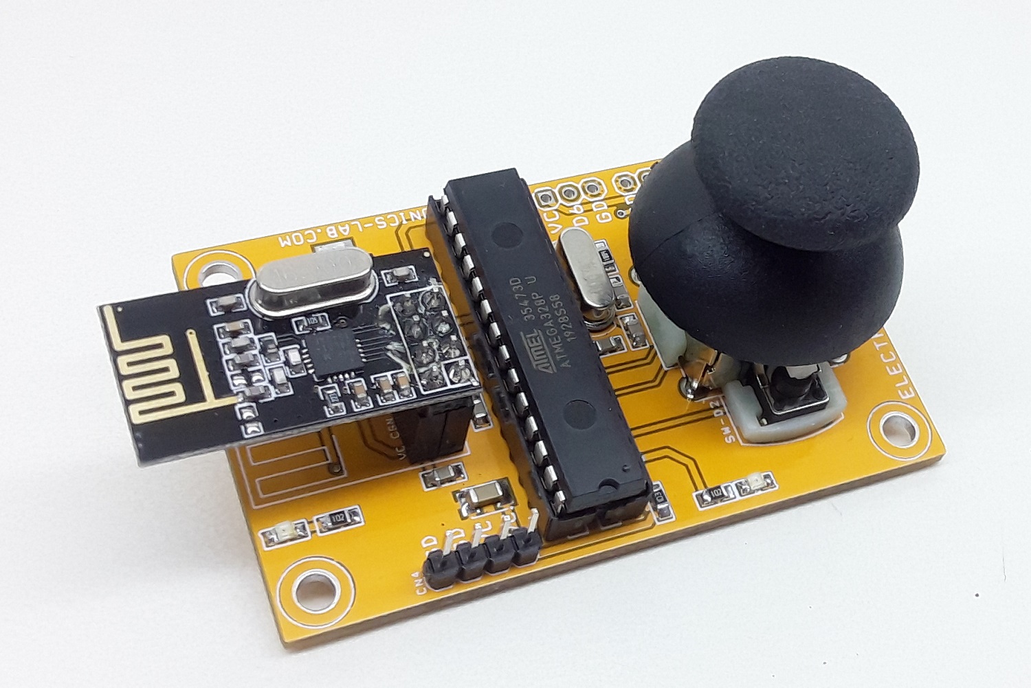
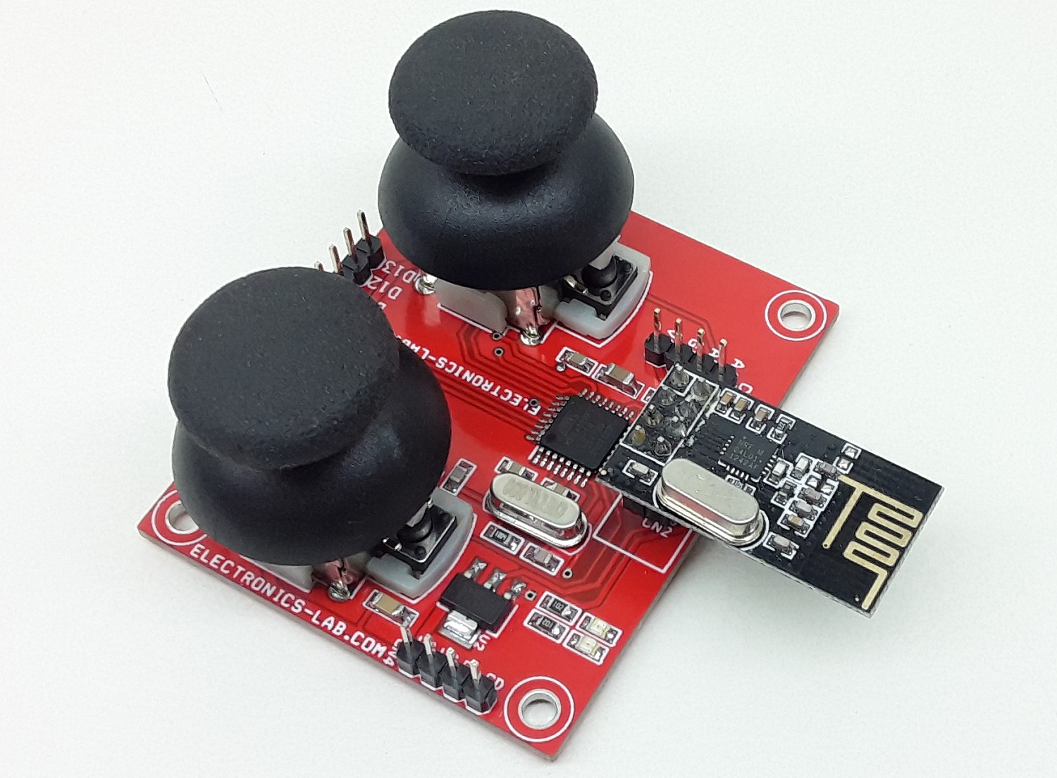
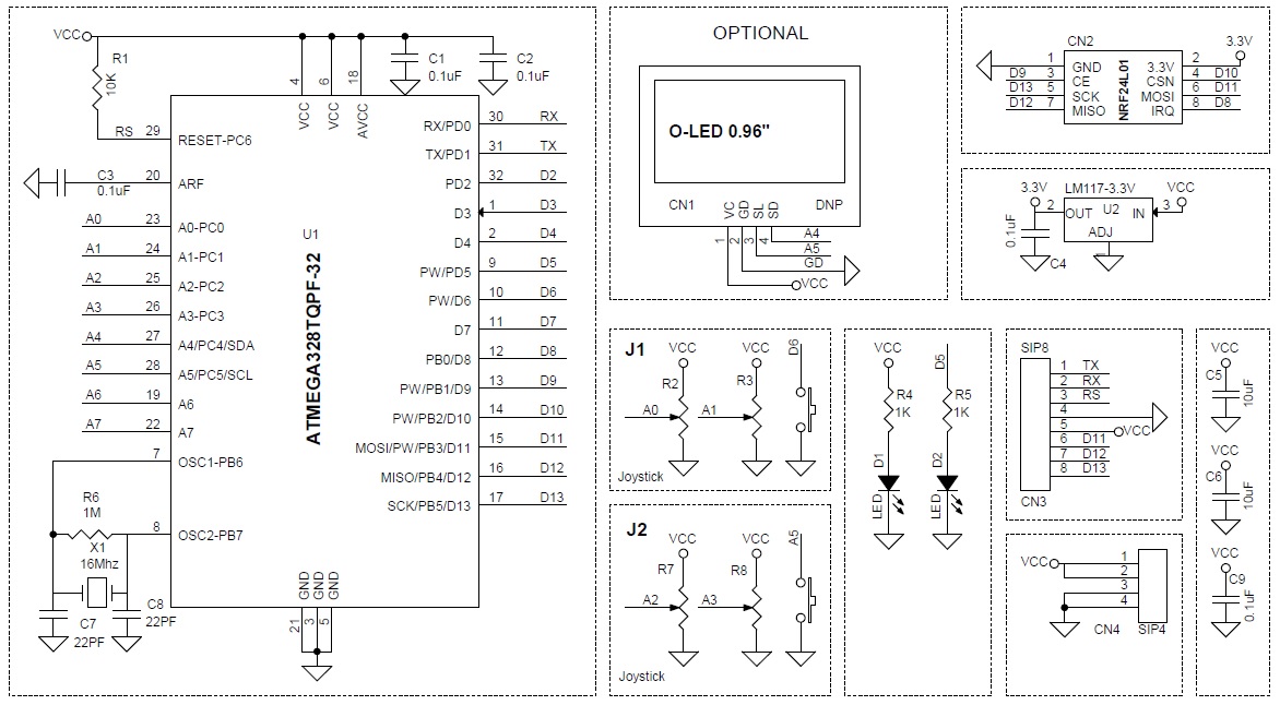
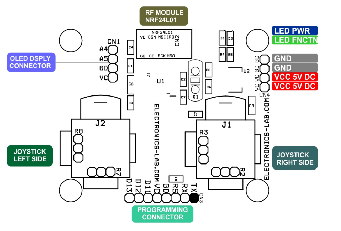
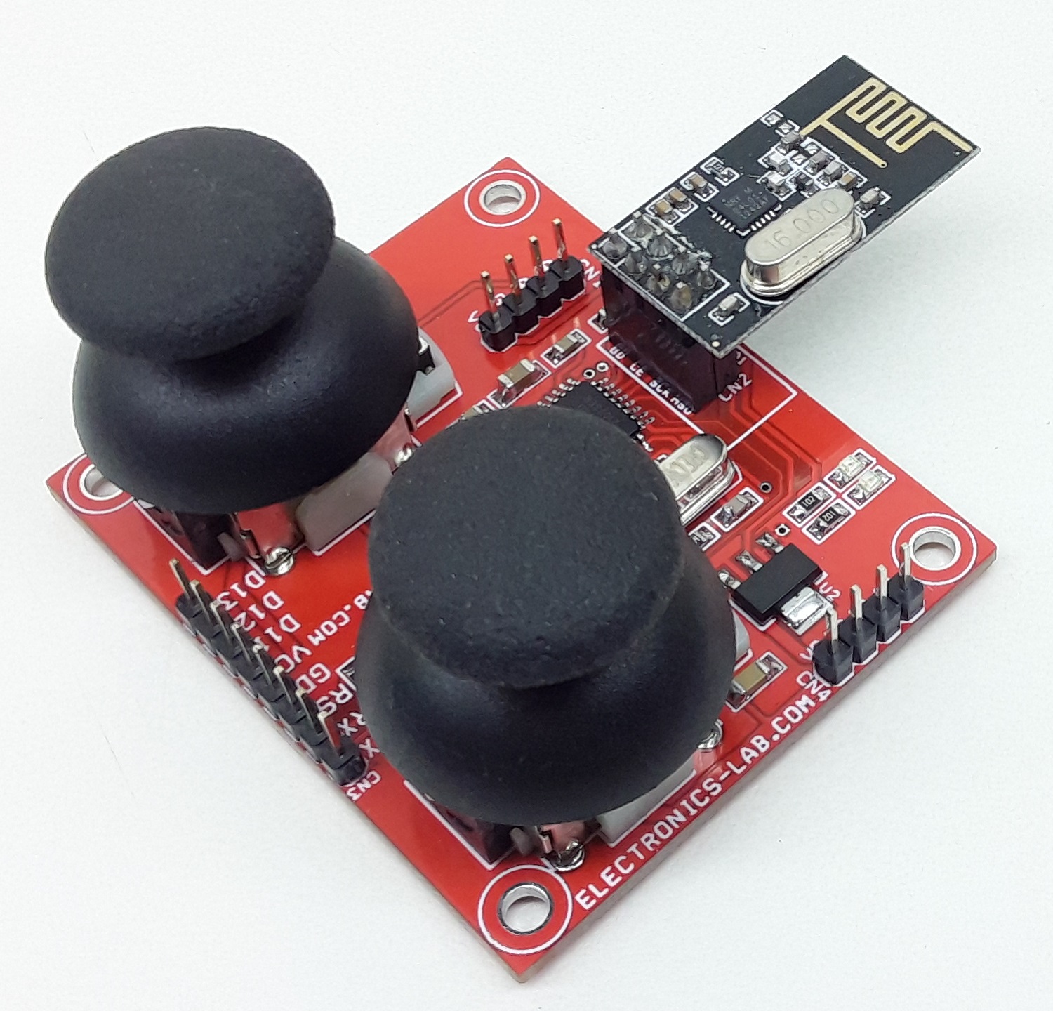
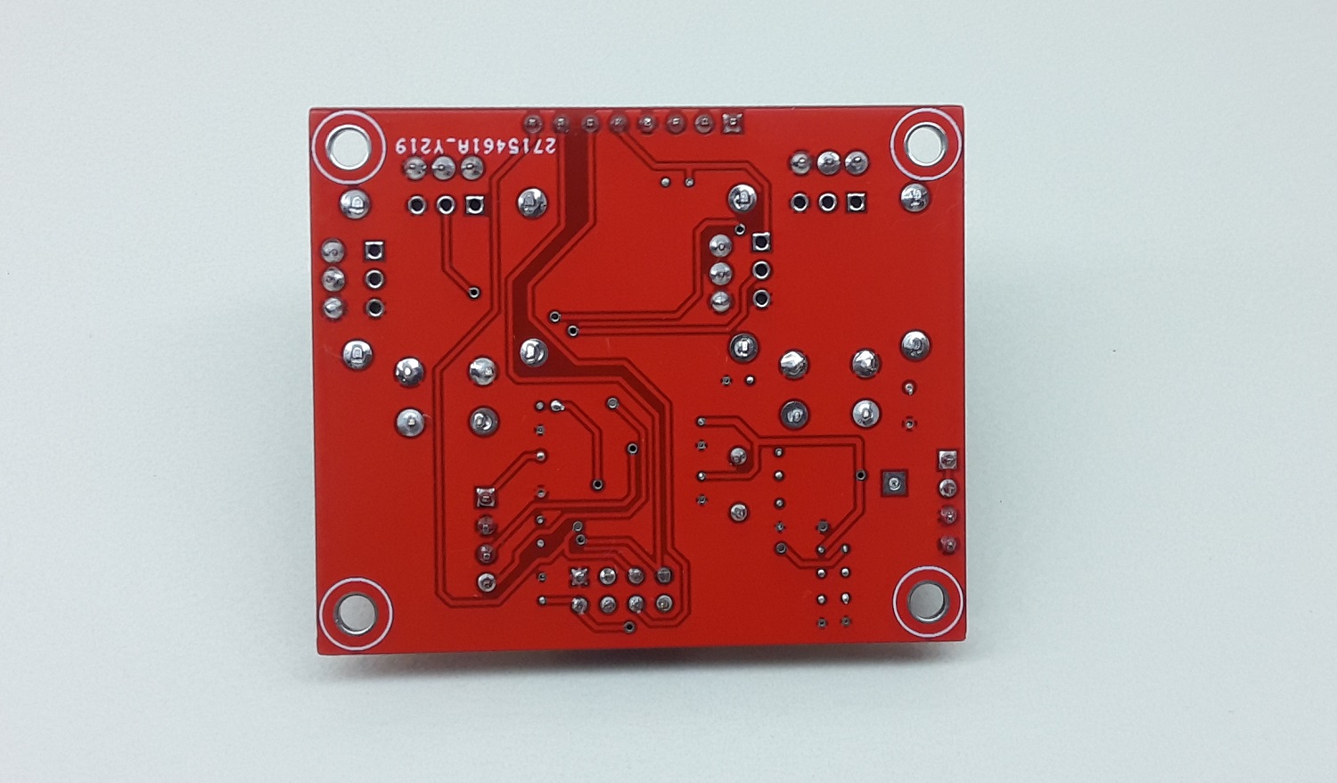
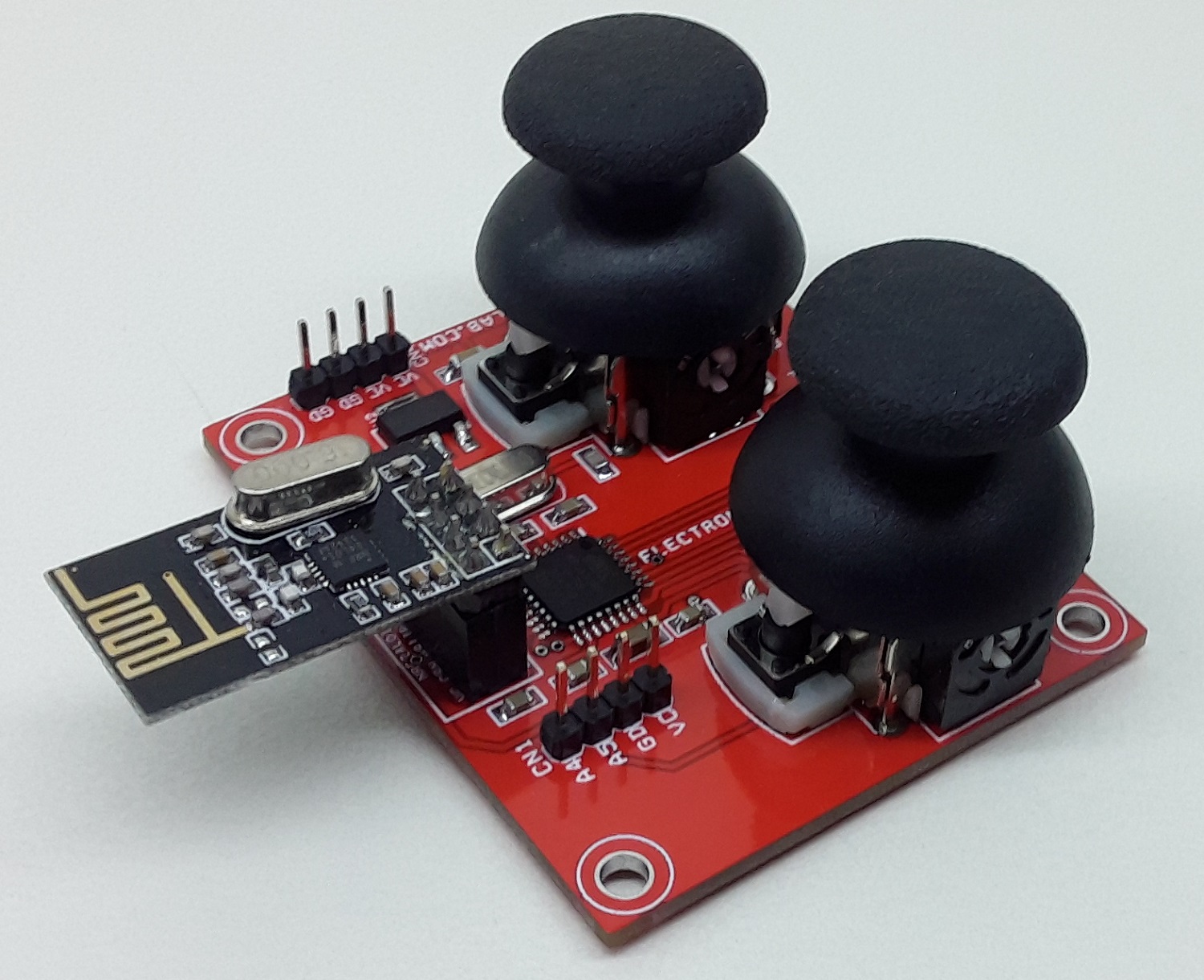
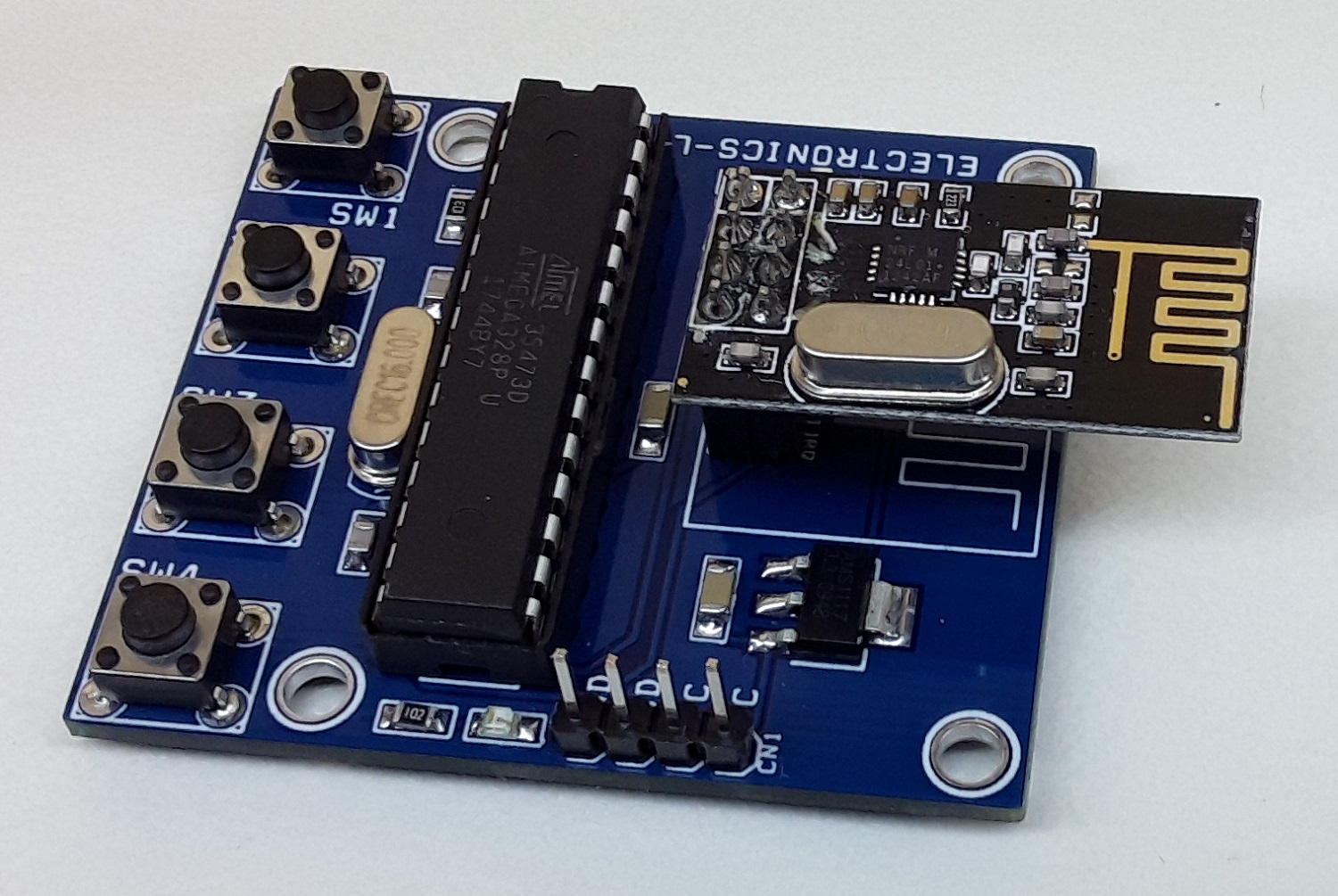
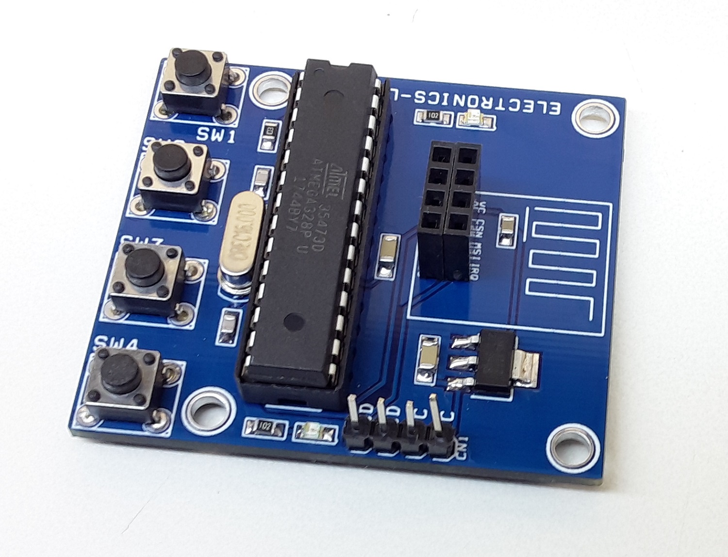
This is an Arduino compatible open-source hardware that includes 1 x joystick, NRF24L01 RF module, Atmega328D microcontroller, 3.3V regulator, power LED, function LED, and other required components. This board can be used for the development of various applications such as Gaming, Remote RC servo driver, RC Motor controller, Robotics, and many more.
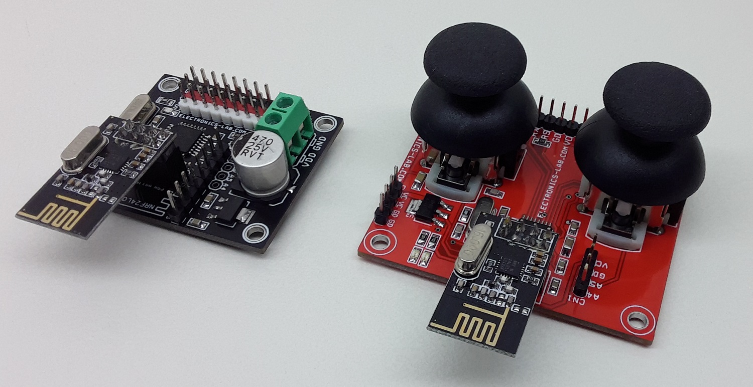
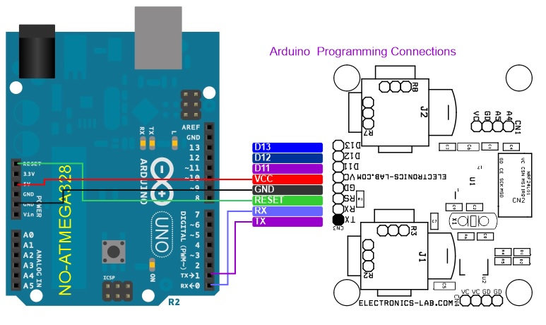
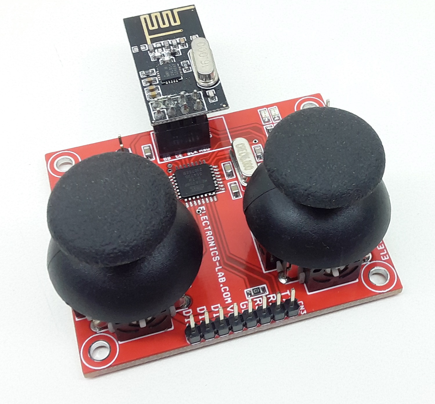
This is an Arduino compatible open-source hardware that includes 2 x Joysticks, NRF24L01 RF module, Atmega328 microcontroller, 3.3V regulator, power LED, function LED, Arduino programming connector, and other required components. This board can be used for the development of various applications such as Gaming, Remote RC servo driver, Robotics, and many more. Connector CN3 was provided to program the ATMEGA328 microcontroller using Arduino IDE.
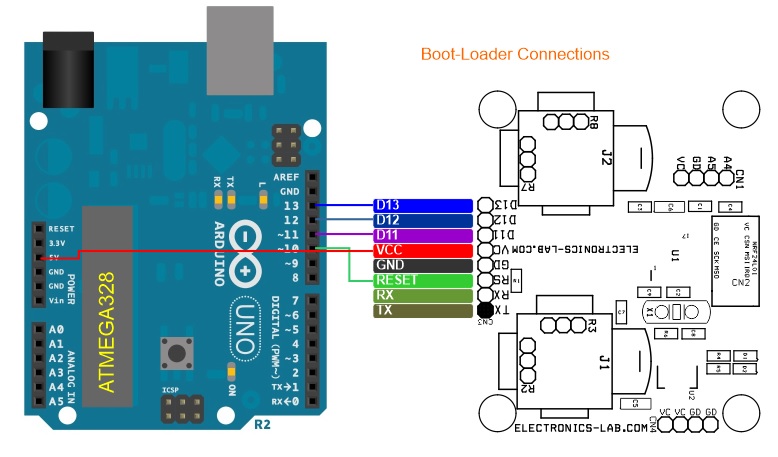
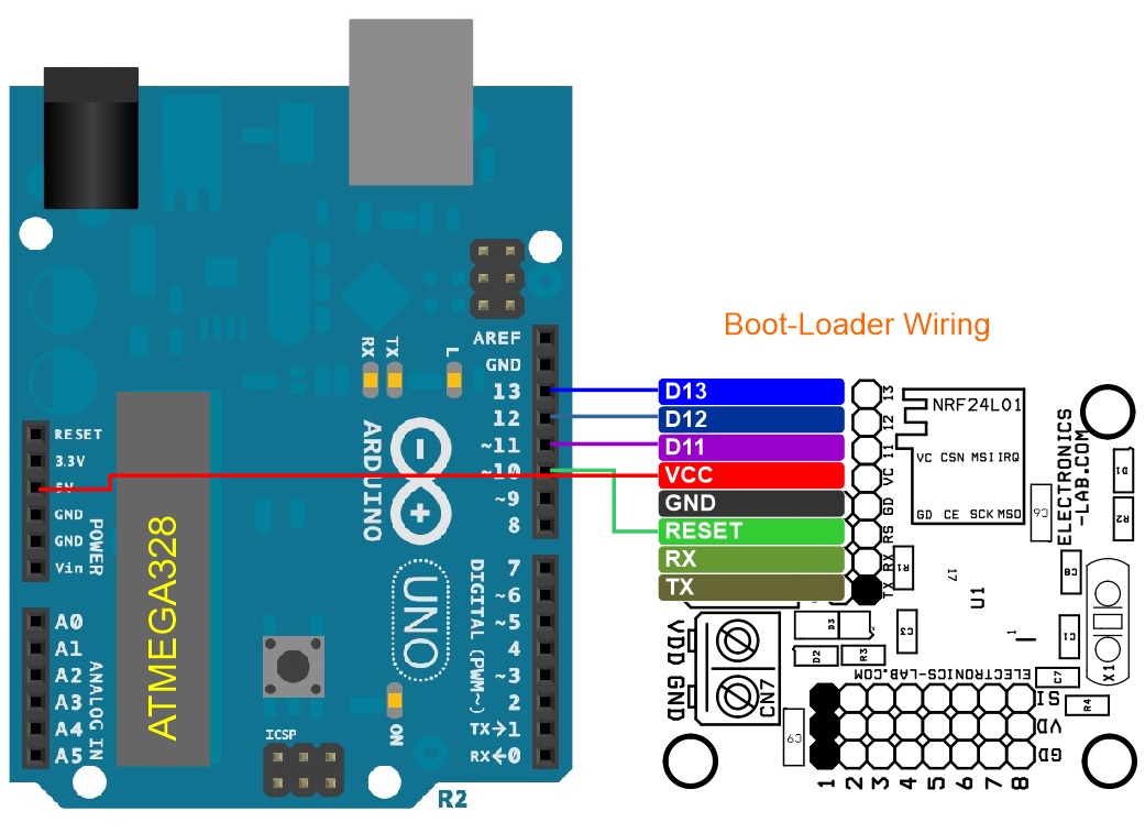
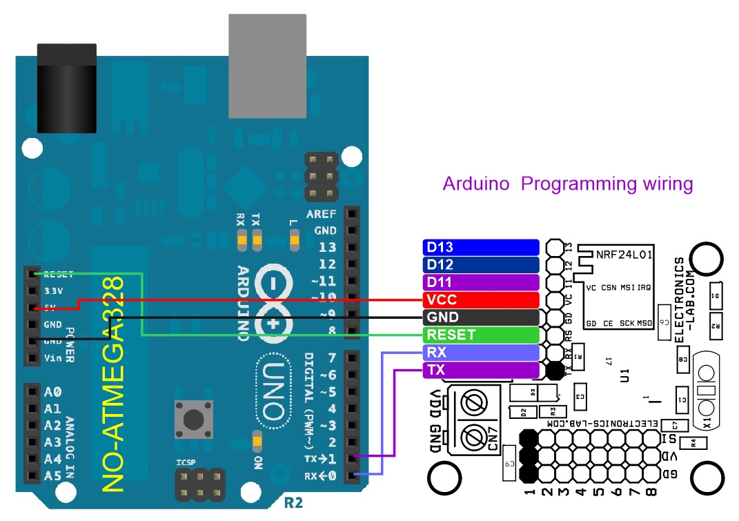
A new ATMEGA328 microcontroller requires a bootloader to be programmed using Arduino IDE and then upload the firmware, more information is available here:
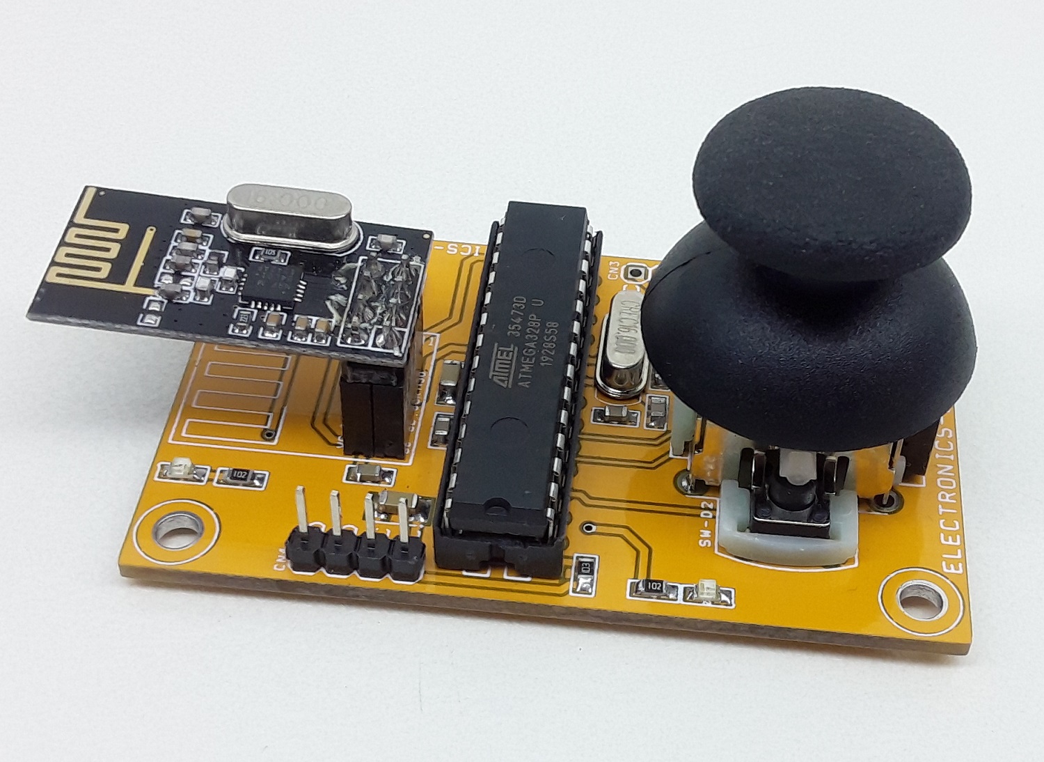
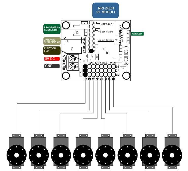
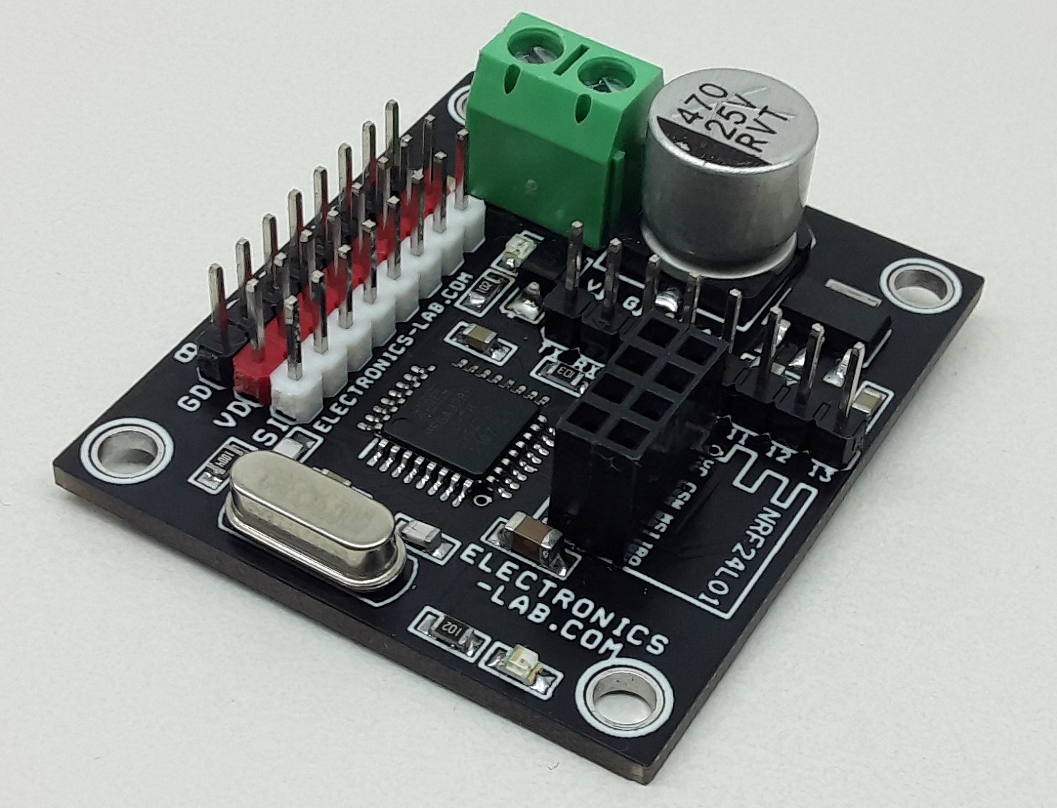
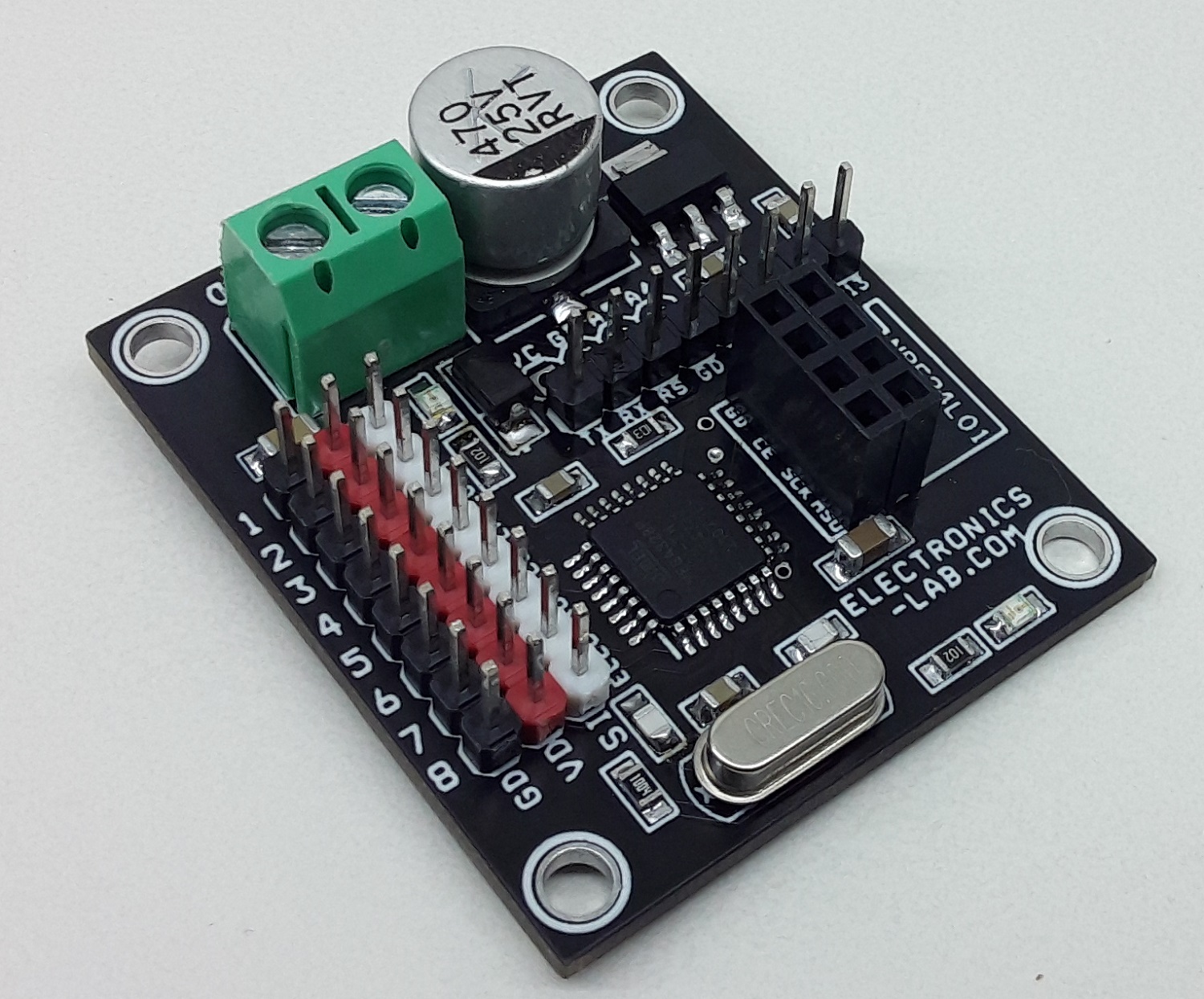
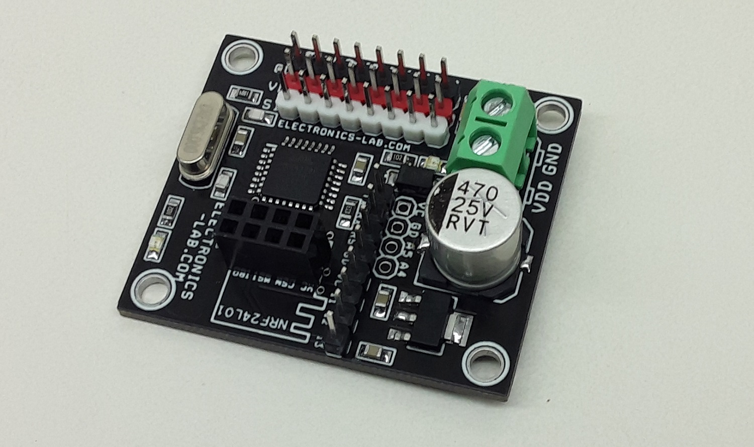
This is an easy-to-build open-source Arduino compatible board that enables driving 8 RC servos over NRF24L01 RF Link. The project can be used as a standalone RC servo driver or 8 channel RF remote-controlled RC servo Receiver. An optional OLED display option can be used to develop RC signal monitor. The tiny module contains an ATmega328 microcontroller, connectors for 8 x Servo interface, DC supply connector, bulk electrolytic capacitor C5 on DC supply to provide jitter-free smooth movement of RC servos. Operating Supply 5V DC.
RF Remote Controlled 8 Channel RC Servo Receiver and Controller
RC Signal Monitor Reader
3 Channel PWM Output Over NRF24L01 RF Link (Arduino Digital Pin D3, D5, D6)
Code
A new Atmega328 microcontroller requires a bootloader and Arduino code. Connector CN4 is provided to do needful, the bellow link will help you to learn more about programming and boot-loader burning.
Arduino Code is available below as a download for both RX and TX. A compatible transmitter board is published here. This is Arduino compatible hardware. User may write their own code using Arduino IDE. Code can be uploaded to the board using the CN4 programming connector following the connection diagram below.
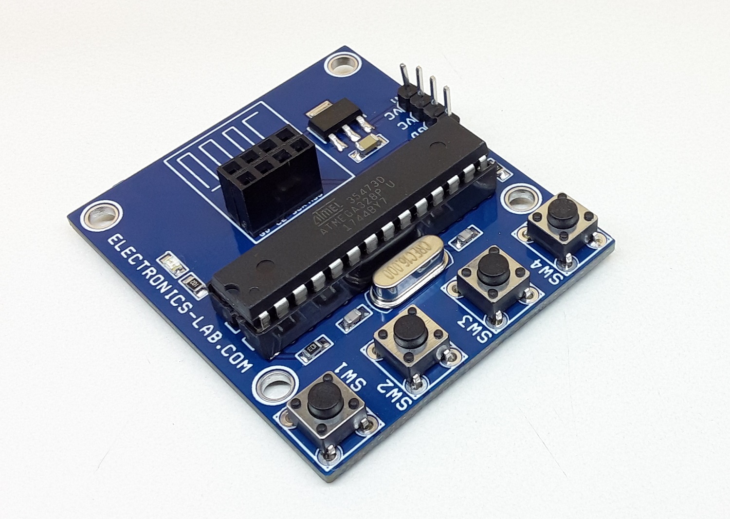
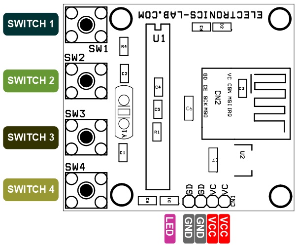
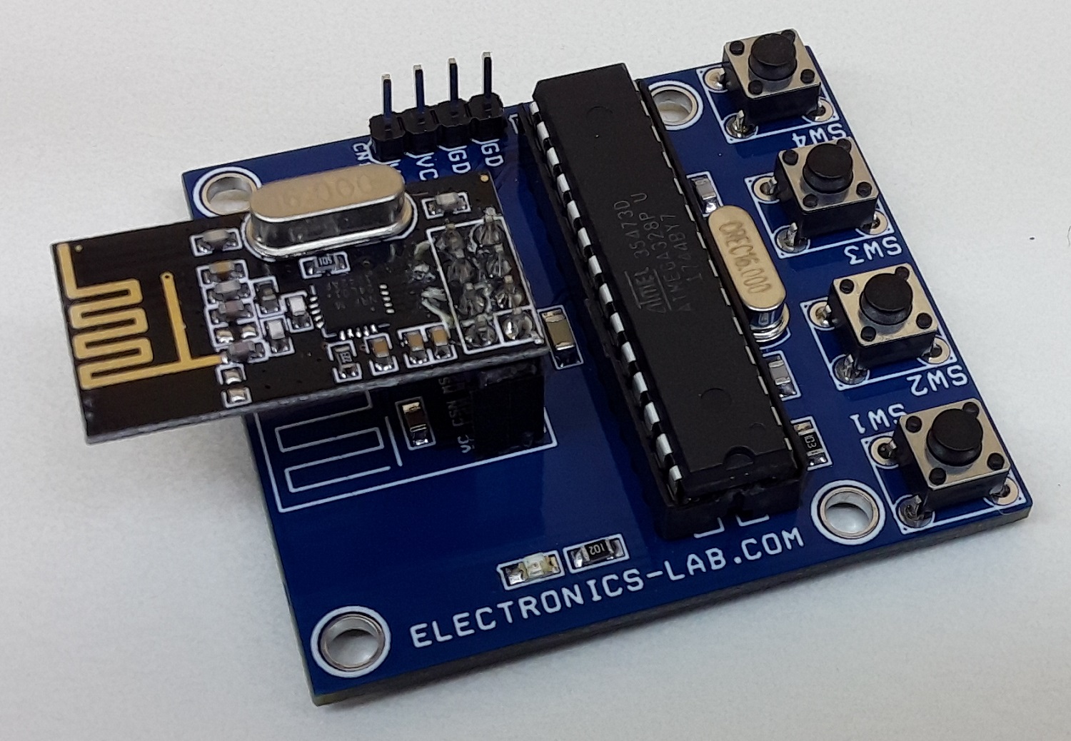
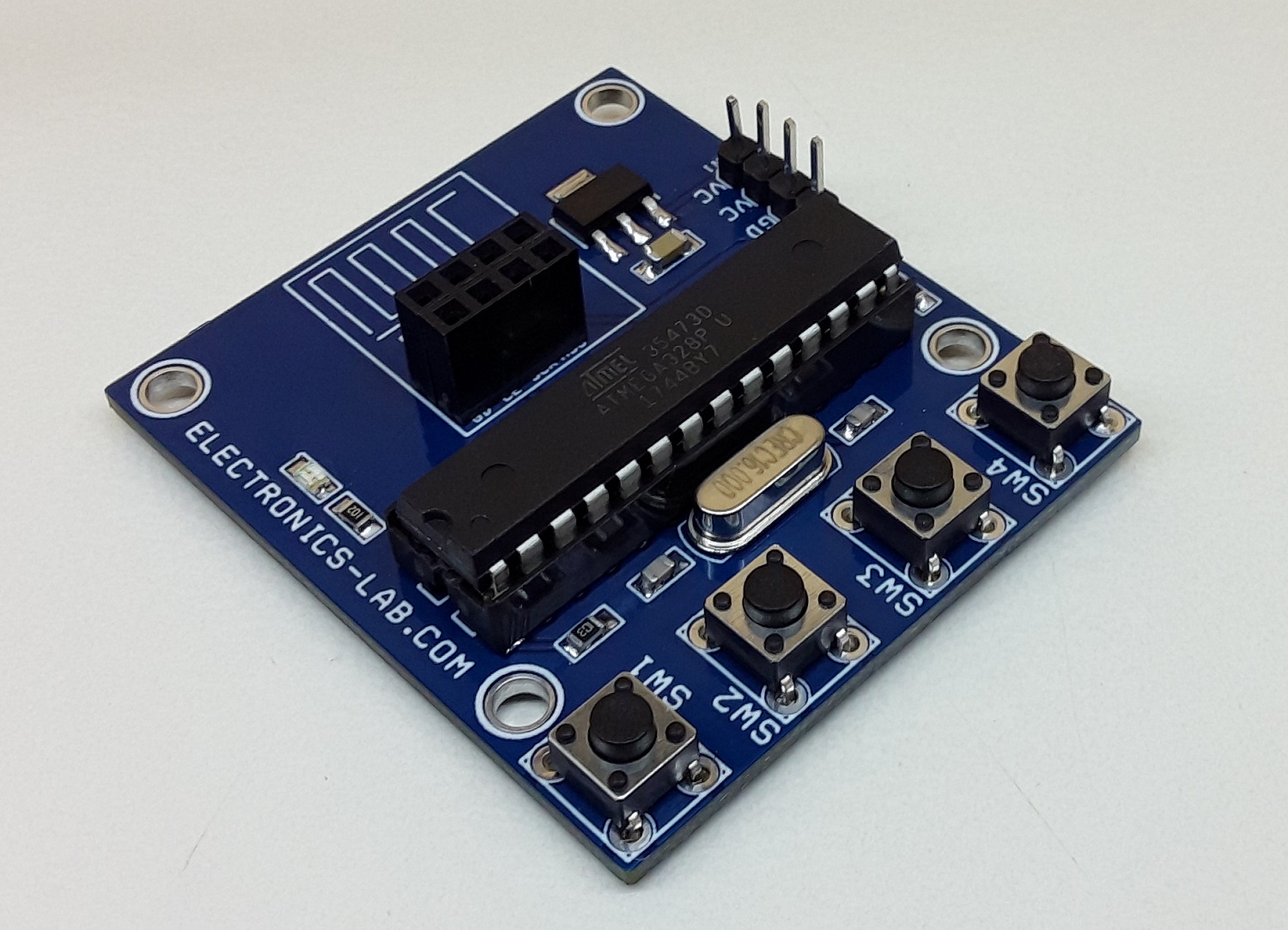
This is an open-source Arduino compatible board that enables you to build a 4 channel RF remote control. The project consists of an Atmega328 microcontroller, 4 tactile switches, nRF24L01 2.4Gz RF Transceiver Module, power LED, function LED, and 3.3V regulator. The operating supply is 5V DC. All switches are connected between Arduino pins and GND and they can be used with internal pull-up resistors. The receiver can be an Arduino UNO with the following PIN configurations. A suitable receiver board will be published soon.
Transmitter
TX Arduino Pins
Switch 1>> Digital Pin D2
Switch 2 >>Digital Pin D3
Switch 3 >>Digital Pin D4
Switch 4 >>Digital Pin D5
LED D1 >> Digital Pin D6
TX NDRF24L01 Transceiver Module
CE>> Digital pin D9
CSN>> Digital pin D10
MOSI>> Digital pin D11
MISO>> Digital pin D12
SCK>> Digital pin D13
IRQ>> Digital pin D8
3V and GND
Receiver
RX Arduino UNO Pins Outputs
Digital Pin D2
Digital Pin D3
Digital Pin D4
Digital Pin D5
NRF24L01 Transceiver Module on Arduino Uno RX
CE>> Digital pin D9
CSN>> Digital pin D10
MOSI>> Digital pin D11
MISO>> Digital pin D12
SCK>> Digital pin D13
IRQ>> Digital pin D8
3.3V and GND
Specifications
Power supply: 5Vdc
Onboard status LED
PCB dimensions: 49.85 x 44.29 mm
Code
Arduino code is available as a download, which will help users to test this board. Please note that it requires a 2nd Arduino and an additional nRF24L01 module as receiver to test the TX board. Both transmitter and receiver codes are provided. A new Atmega328 microcontroller will need the Bootloader and Arduino firmware, check the link below to learn more.
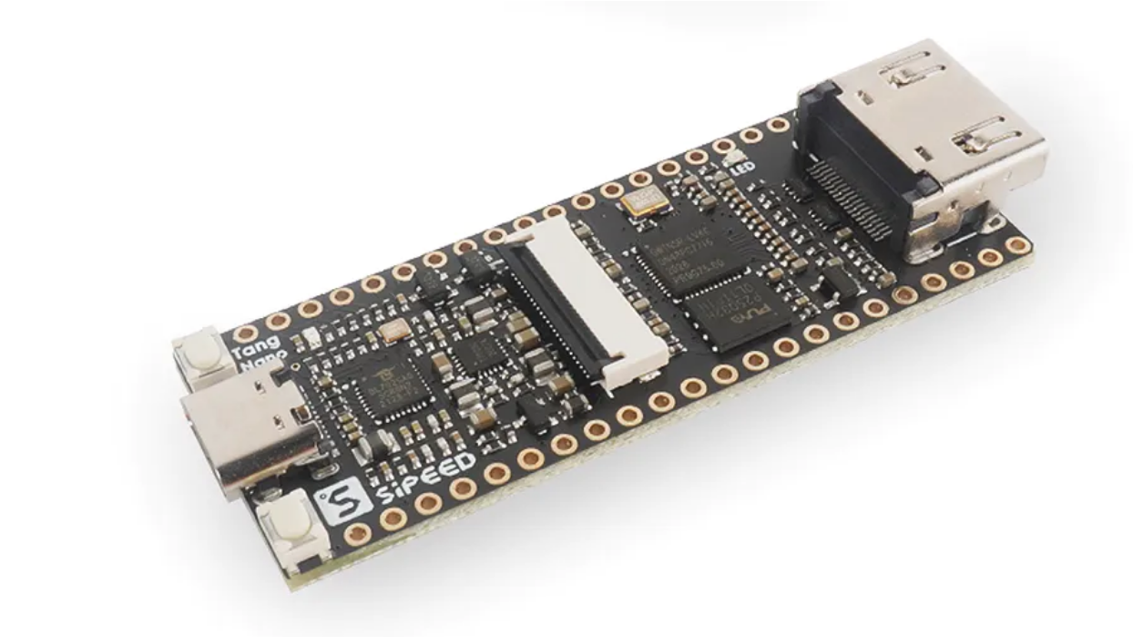
There had been a spoiler by Sipeed a few weeks back about the testing of yet another Tang Nano board. Yes, you are right, this is not the first Tang Nano board by Sipeed, but the first version came two years ago as a $5 development board built around Gowin GW1N-1 LittleBee FPGA. Electronic hardware leader Sipeed has released the Tang Nano 4K board featuring Gowin Semiconductor’s LittleBee series GW1NSR-LV4C FPGA.
The board has a powerful upgraded version of the Gowin’s LittleBee FPGA and a hardcore processor of Arm Cortex-M3 that was missing from its predecessor. Also, when compared to the first release of Tang Nano, the new module has 4608 LUTs which is more than 4 times. Tang Nano 4K board features significantly more registers to 3456 compared to 864 in its predecessor.
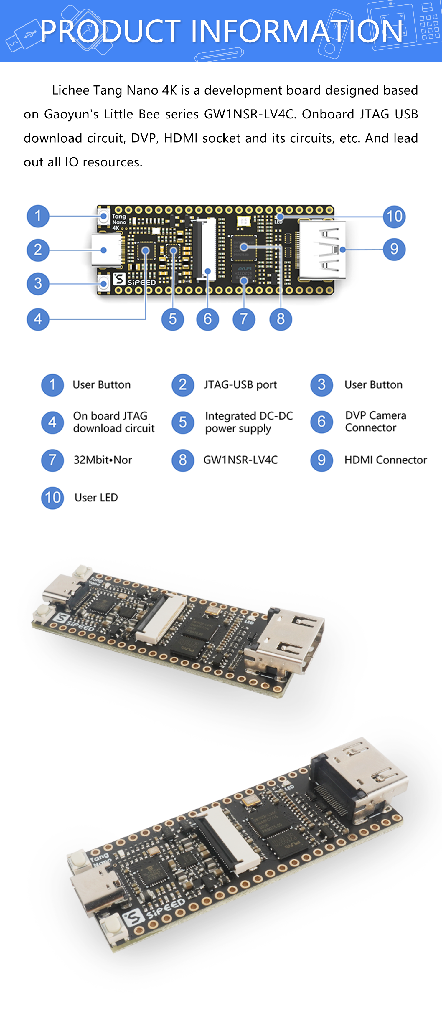
Specifications of Tang Nano 4K Board:
FPGA: Gowin GW1NSR-LV4C
LUTS: 4608
Register: 3456
Multiple Parameters: 16
SRAM: 180K
Flash memory: 256K
PLL: 2
Total I/O bank: 4
Processor: Arm Cortex-M3
Camera interface: OV2640
Display interface: HDMI
Dimensions: 60mm x 22.86mm
Power: USB Type-C port
With its minimalistic design, the board is shipped with camera and display interfaces via default OV2640 interface and HDMI respectively. However, with the 32-bit Arm processor, you can expect decent performance with a slight delay in video interfacing. Note that the manufacturer is not too sure if the HDMI interface can do video-in as the Gowin official demo is for output. Also, the HDMI interface is capable of giving a maximum video resolution of up to 720p.
The hardware gets the maker-friendly USB Type-C port to power the board. Also, if you are interested in learning more about the integrated FPGA, visit the datasheet here. The manufacturer has provided a GitHub repository for contributing open source projects on the Tang Nano 4K board. If you purchase the sub-$15 board, I would suggest contributing to the GitHub repository that can help others get started with the hardware.
Sipeed clarifies that the baseboard is priced at $12 and if you wish to get it with OV2640 then it will be available at $15.
The conventional style of using network connectivity in bringing artificial intelligence models to improve performance and efficiency needs some modification to meet the demands from the embedded systems to the automobile industry. Before directly jumping to the role of AI inference at the edge, let us understand the difference between training and inference. Machine learning training refers to the process of building an algorithm with frameworks and datasets, while in the case of inference, it takes the trained machine learning algorithms to make a prediction.
By getting AI inference at the edge, there is a significant improvement in the performance along with the reduced time (inference time) and reducing the dependency on the network connectivity.
Machine learning or artificial intelligence inference can run in on the cloud as well as on a device (hardware). However, when there is a requirement for fast data processing and predictions of the outcome, AI inference at the cloud can increase the inference time creating delays in the system. For non-time critical applications, AI inference at the cloud can always do the job, but in a world full of IoT devices and applications that require fast processing, AI inference at the edge solves the problem. In AI inference at the edge, specialized models are made to run at the point of data capture, which is an electronic embedded device in this case.
A look at the famous AI inference at edge hardware
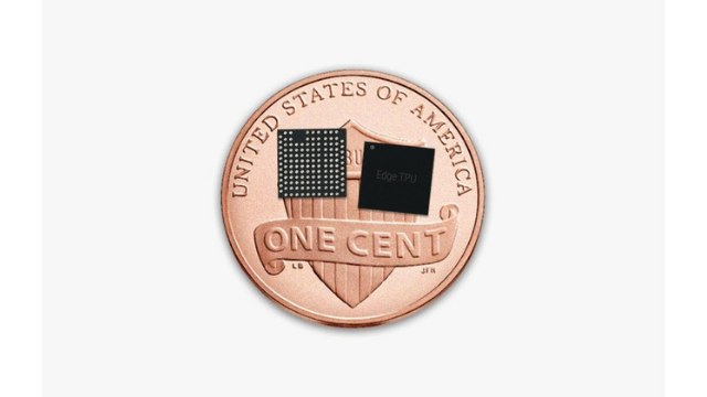
Google Edge TPU
Image Credits: Google Cloud
Google Edge TPU is Google’s custom-built ASIC that is designed to run AI at the edge with a target for a specific kind of application. When we talk about TPUs, CPUs and GPUs, it is important to note that only TPU is an ASIC while the other two are not. Also, in TPUs, the ALUs are directly connected to each other without using memory. This means that there is a low latency in transferring information.
With the need and increasing requirements to deploy high-quality AI inference at the edge, there have been several prototyping and production products from Coral that come with integrated Google Edge TPU. This small ASIC is built for low-power devices that can execute state-of-the-art mobile vision models such as MobileNet V2 at almost 400 FPS, in a power-efficient manner. According to the manufacturer, an individual Edge TPU can perform 4 trillion operations per second (4 TOPS), while utilizing only 2 watts of power. More information on ASIC and the production products can be found on the manufacturer’s page.
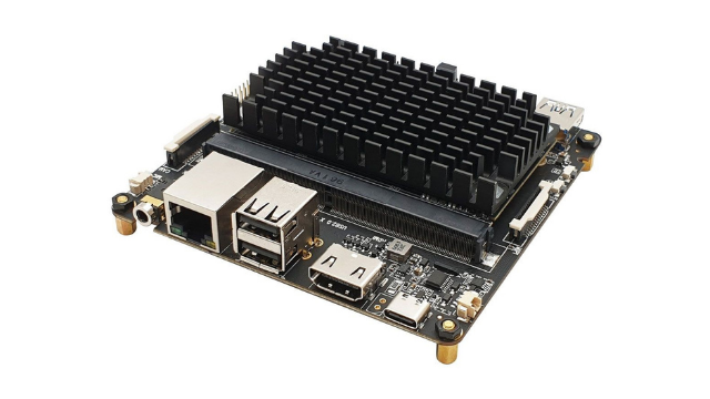
Rock Pi N10
Image Credits: Seeed Studio
If you are interested in deploying AI or deep learning at the edge and looking for a single-board computer. This Rock Pi N10 can serve the purpose through the powerful Rockchip’s RK3399Pro SoC integrated by CPU, NPU, and GPU. The CPU features Dual Cortex-A72 running at the frequency of 1.8GHz and quad Cortex-A53 clocked up to frequency 1.4GHz. NPU has the power of computing up to 3.0 TOPS, especially for AI and deep learning processing. NPU is assumed to have decent performance for complex calculation and processing that can be deployed for AI and deep learning applications.
Once you buy this SBC, here is a detailed guide on how to get the Rock Pi N10 up and running with the NPU inference. The hardware has software support for Debian and Android 8.1 OS. You can also expand the storage using the M.2 SSD connector that supports up to 2TB SSD. However, before you get the hardware for your AI inference at the edge, please note that the SBC does not come with onboard Wi-Fi support, but you can get an optional Wi-Fi module to be embedded on the board. Find more details on the Seeed Studio product page.
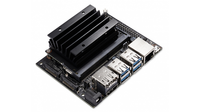
NVIDIA Jetson Nano Developer Kit
Image Credits: NVIDIA
One of the most powerful hardware designed for AI applications is the NVIDIA Jetson Nano Developer Kit that features a small, powerful computer that lets you run multiple neural networks in parallel with applications like image classification, object detection, and speech processing. The hardware also gets support for AWS ML IoT services, with this you can easily develop deep learning models and deploy them on the edge. The manufacturer has also provided deep learning inference benchmarks that will help you decide if the hardware is best suited for your application and requirements.
With the developer kit, the user can run various ML frameworks, including TensorFlow, PyTorch,Caffe/Caffe2, Keras, and MXNet. NVIDIA Jetson Nano developer kit comes with the Quad-core ARM A57 that runs at the clock frequency of 1.43 GHz and a 128-core NVIDIA Maxwell GPU. This model is one of the leading hardware for deploying AI inference at the edge. For more information on the hardware, head to the official product page.
Future of AI inference at the edge
The undisputed fact is that AI computing at the edge brings processing and data storage closer to the source. The future of Edge AI computing lies in an autonomous vehicle system where edge AI hardware takes data from the surroundings, processes it, and makes the decision there itself. This is a major advantage of AI inference at the edge over cloud processing where it can take longer processing time. Overall, the future of AI inference at the edge is bright with the growing AI requirements and fast processing of data using deep learning models.
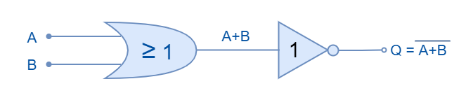
The logic NOR gate is the reverse or complement form of the logic OR gate which was discussed in the previous article. Similar to the logic NAND gate, it is a series combination of logic OR gate and an inverter thus forming a logic NOR gate. The logic NOR gate equivalent is shown in the following figure.
Figure 1: The logic NOR equivalent circuit
The logic NOR gate’s output becomes “HIGH” only when both of its inputs are at “LOW” states and for the rest of the states, the output will be in “LOW” level state. This is in exact contradiction to the logic function performed by the OR gate and because of this contradiction, it is called Not-OR (NOR).
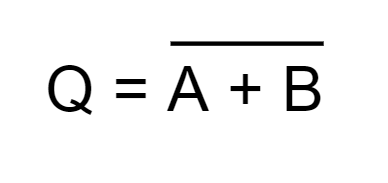
In Boolean algebraic or logical expression, the logic NOR is a form of multiplication that is performed on the complements of the inputs. The expression of logic NOR is denoted by a plus (+) sign between the operands (inputs) and has an overline. Whereas, the overline represents an inversion of the logic OR. The expression for the two-inputs NOR gate is given below:
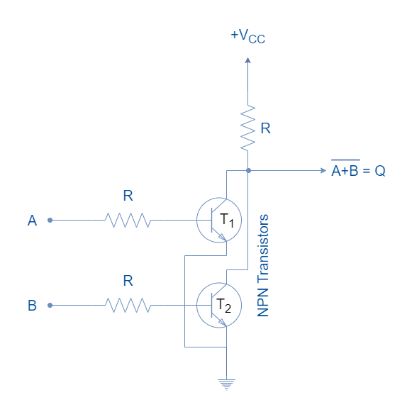
Resistor-Transistor NOR Gate
In the following figure, a basic two-input NOR gate constructed using Resistor-Transistor Logic (RTL) is shown.
Figure 2: The Resistor-Transistor Logic NOR Gate
When both inputs “A” and “B” are “LOW” then both transistors are in saturated “OFF” states and a state “HIGH” appears at the output (Q). Turning any of the inputs to logic “HIGH” will drive the relative transistor to the “ON” state and thus completing the path from VCC to Ground through a resistor (R). Which gives a state “LOW” at the output (Q).
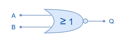
Logic NOR Gate Symbol & Truth Tables
The representation of a NOR logic by a symbol is shown in the following figure. An inversion bubble at the output denotes the inversion of the multiplication.
Figure 3: Logic NOR Gate Symbol
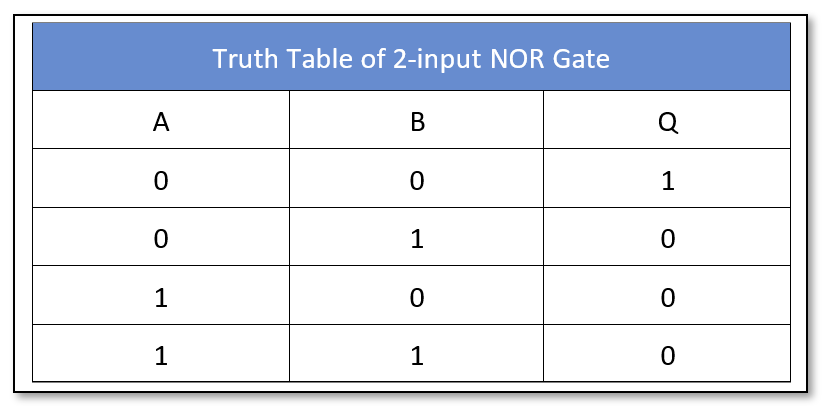
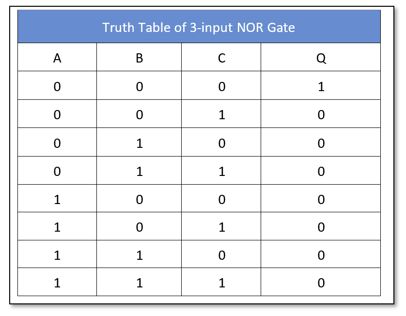
The truth table of a two-input NOR logic gate is shown below:
Similarly, the truth table of a three-input NOR logic gate is as follow:
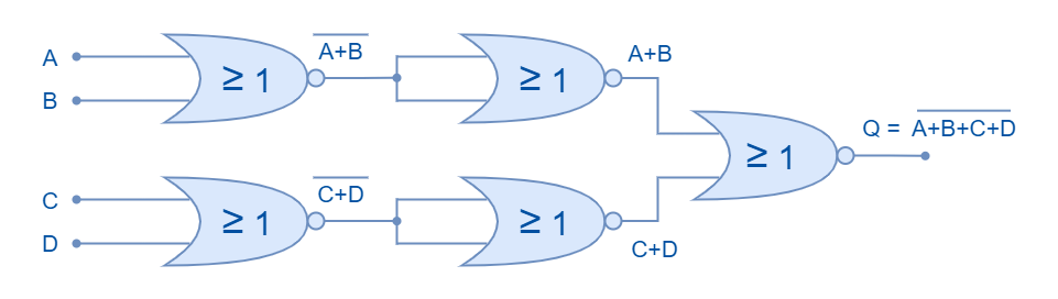
The Boolean expression can be extended to include multiple inputs to obtain NOR logic operation. However, commercially available NOR logic circuits have up to four inputs but the number of inputs can be further extended by cascading the NOR logic circuits. In the following figure, five two-inputs NOR gates are cascaded together to obtain a four-input NOR logic function.
Figure 4: A 4-input NOR logic constructed by cascading multiple NOR gates
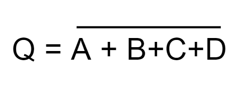
The Boolean expression for this cascaded circuit can be written as:
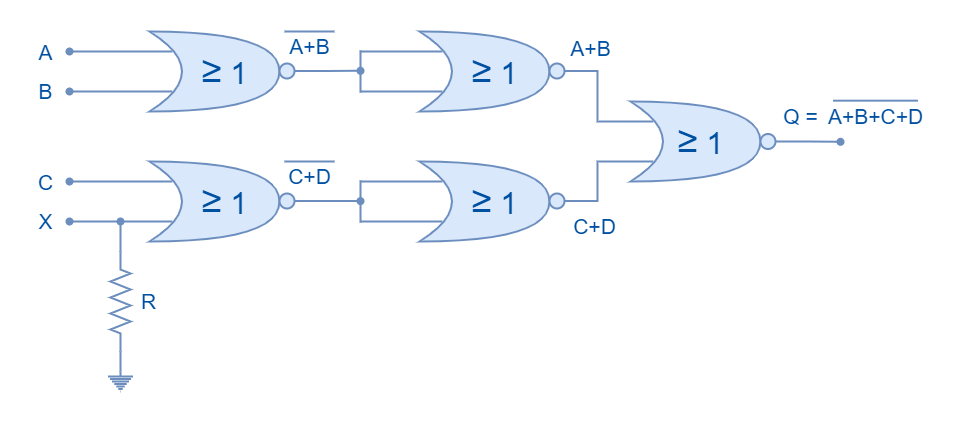
Odd Number of Inputs
The NOR logic circuit having an odd number of inputs can be constructed by driving the unused input to logic “LOW” or ground through a pull-down resistor. This will ensure that another input(s) of the NOR logic gate is truly reflected at the output. It is explained in the following diagram where unused input is pulled down using a pull-down resistor.
Figure 5: The NOR logic having an odd number of inputs
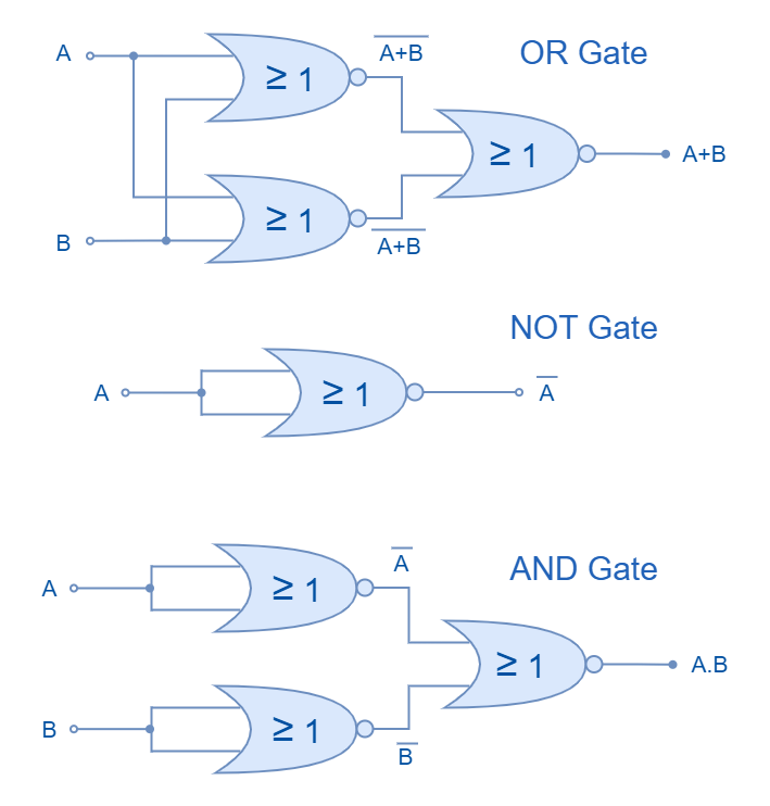
Universal Gate
Similar to the logic NAND gate, the logic NOR gate also exhibits the universal logic characteristics i.e. other logic gates can be constructed by forming the different combinations of logic NOR gates. Besides basic logic gates (AND, OR & OR), exclusive-OR and exclusive-NOR gates can also be constructed using universal gates. The examples of forming the AND, OR, and NOT logic by using NOR gates are shown in the following figure.
Figure 6: Construction of logic gates using universal NOR gate
Commercially Available NOR Gates
The NOR logic gates are available in both TTL and CMOS logic families. The most commonly used NOR logic packages are:
CMOS based NOR Gate IC Package
CD4001 Quad 2-input
CD4025 Triple 3-input
CD4002 Dual 4-inputs
TTL based NOR Gate IC Package
74LS02 Quad 2-input
74LS27 Triple 3-input
74LS260 Dual 4-input
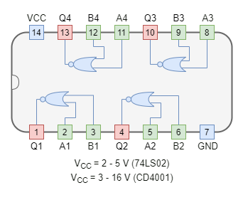
Figure 7: 74LS02 & CD4001 Package having 2-input quad NOR gates
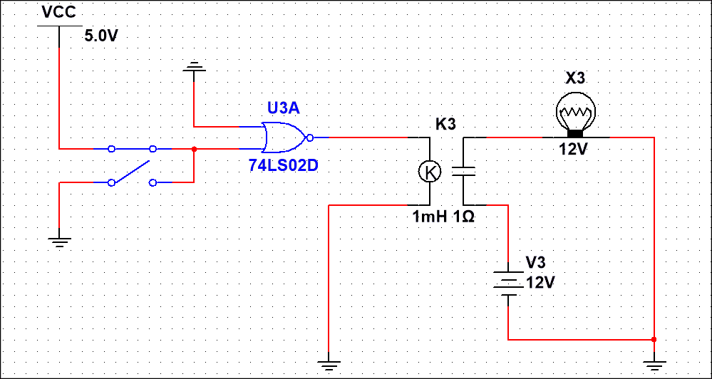
Example of NAND Logic
In the following figure, a NOR gate is used to drive a 12V relay to switch on the lamp using NI Multisim. The NOR gate (74LS02) turns on the relay when all of the inputs are connected to Ground/ 0 V. The relay thus turns on the lamp through an external circuit of 12V. When any of the input is connected to VCC, NOR logic goes “OFF” turning the relay and lamp to “OFF” state.
Figure 8: A Multisim circuit showing NOR logic to control an external circuit
Conclusion
The output of the NOR logic is “HIGH” when all of the inputs are in logic “LOW” states.
Any of the inputs in the logic “HIGH” state will drive NOR logic to the “OFF” state.
The NOR logic gates can be constructed using Resistor-Transistor Logic (RTL) but are seldom used because of the propagation delay and power consumption.
The NOR gate is termed a Universal Gate because of its capability to form any other logic using only NOR gates.
The logic NOR gates commercially available have up to four NAND logic inputs. However, inputs can be extended by using cascaded NOR logic gates.
The NOR logic circuit having an odd number of inputs can be constructed by using a pull-down resistor on the unused pin.
An external circuit can be controlled by NOR logic with the use of a magnetic relay.