Molex Disposable Thin-Film Battery stocked by Heilind Electronics

Heilind Electronics, a leading global distributor of electronic components and authorized global distributor for Molex, has expanded its selection of electronic component solutions with the company’s disposable thin-film battery.

The thin-film batteries are zinc-carbon primary cells (Zn anode/MnO2 cathode) that nominally deliver either 1.5 or 3.0 volts. Typical applications include single-use or disposable sensing and monitoring devices where lightweight, thin form factor and flexibility are desired.

The vertical construction reduces the footprint compared to other printed batteries and leads to lower internal resistance and improved performance. These thin-film batteries can be applied in a curved surface with a bend radius of 25 mm or greater. The 1.5 V and 3 V batteries support design flexibility and reduce the distance between anode and cathode. They operate at a temperature range of minus 35 degrees Celsius to plus 50 degrees Celsius.

Features & Benefits

  • No heavy metals – Offers an economical, environmentally safe alternative to lithium
  • Thin, flexible form factor supports design flexibility appropriate for a wide variety of products
  • Flexible and low-profile – Can be applied on a curved surface with a bend radius of 35.00mm or greater
  • Reduced distance between anode and cathode
  • Vertically stacked construction provides the following compared to single-layer construction: reduced internal resistance, increased peak current, increased usable capacity & reduced footprint
  • Available in 1.5 and 3V configurations – Delivers power suitable for low-power disposable application

Video

This solution is made with non-hazardous materials and is designed for low-power single-use applications such as wearable electronics, biometric monitoring devices, biosensors, smart labels and environmental sensors. Molex thin-film batteries are found in a variety of industries, including medical, industrial, IoT, and consumer.

For more information, visit heilind.com

EV35L43A AVR128DB48 Curiosity Nano Evaluation Kit

Microchip Technology’s AVR128DB48 is a development board that users can keep in their pocket

Users can take their next idea to market with a Microchip Technology development board that can be kept in a pocket. With full program and debug capabilities, the AVR128DB48 Curiosity Nano evaluation kit offers complete support for the next design.

Use either Atmel Studio 7 or MPLAB7® X IDEs as a magnifying glass to investigate MCU and step through the debug. Free, easy-to-use graphical programming tools, Atmel START and MPLAB code configurator (MCC), allow users to program the target MCU intuitively.

  • On-board debugger
    • Board identification in Atmel studio and Microchip MPLAB X
    • One green power and status LED
    • Programming and debugging
    • Virtual serial port (CDC)
    • Two logic analyzer channels (debug GPIO)
  • USB or externally powered
  • Adjustable target voltage
    • MIC5353 LDO regulator controlled by the on-board debugger
    • 1.8 V to 5.1 V output voltage (limited by USB input voltage)
    • 500 mA maximum output curren
  • AVR128DA48 microcontroller
    • Multi-voltage I/O (MVIO)
    • Three integrated operational amplifiers (op amps)
  • One mechanical user switch
  • One yellow user LED
  • One 32.768 kHz crystal
  • One 16 MHz crystal

more information: https://www.microchip.com/en-us/development-tool/EV35L43A

BM2SC12xFP2-LBZ Quasi-Resonant AC/DC Converter

ROHM’s BM2SC12xFP2-LBZ quasi-resonant AC/DC converter with built-in 1700 V SiC-MOSFET features a wide input voltage range.

ROHM’s large current integrated FET type switching regulators are compatible with virtually all switching power supply applications. Features include a wide input voltage range, flexible operating frequency, and low power consumption.

The broad lineup includes boost (step-up) regulators, buck (step-down) regulators, buck-boost (step-up/step-down) regulators with integrated FET, and negative voltage types. Microchip combines its excellent power management AC/DC converters with compact switches, allowing users to save valuable space and reduce the number of components required.

Features

  • Long time support product for industrial
  • TO263-7L package
  • Built-in 1700 V/4 A/1.12 Ω SiC MOSFET
  • Quasi-resonant type (low EMI)
  • Frequency reduction function

Typical Application Circuit

Block Diagram

more information: https://www.rohm.com/products/power-management/ac-dc-converters-ics/ac-dc-converters-ics-pwm-qr/bm2sc121fp2-lbz-product

Selectable Output Piezo Sounder Driver from Diodes Incorporated Drives Higher SPL and Longer Runtimes

Diodes Incorporated introduces the PAM8907 piezoelectric sounder driver, for maximizing sound pressure level (SPL) delivery from a ceramic/piezo sounder. The PAM8907 has a built-in synchronous boost converter, which extends SPL in battery-powered systems and outperforms other similar sounder drivers. The device is optimized for use in wireless trackers, industrial alarm systems, medical equipment, and domestic appliances.

The wide 1.8 V to 5.5 V input voltage range supported by the PAM8907 sounder driver enables it to address a broad variety of potential applications. A 22 VPP or 31 VPP output value can be selected (using the GPIO), thereby providing two different SPL options which allow optimized performance for SPL or battery runtime. Its integrated boost converter requires only a 1.0 µH external inductor which helps reduce the bill-of-materials costs and board space.

Features

  • Supply Voltage Range from 1.8V to 5.5V
  • Intergraded Boost Converter VOUT = 11V or 15.6V
  • Drive Piezo Sounder with up to 31VPP
  • High-Speed Driver Designed with Very Short Turn-On/Turn-Off
  • No Voltage Cross Output at Shutdown Mode
  • High Impendence Output at Shutdown Mode
  • Low Current Consumption, with Shutdown Current < 1μA
  • Automatic Shutdown and Wake-Up Control
  • Available in Space-Saving U-QFN2020-10 package
  • Totally Lead-Free & Fully RoHS Compliant 
  • Halogen and Antimony Free. “Green” Device 

Automatic shutdown and wake-up functions help to further extend the PAM8907 sounder driver’s runtime when incorporated into battery-powered systems, with less than 1 μA of current drawn in shutdown mode. Thermal shutdown, overcurrent, and overvoltage protection, plus undervoltage lockout mechanisms, are included to ensure reliable operation. The product operates across a –40 °C to +125 °C ambient temperature range.

The PAM8907 piezoelectric sounder driver is supplied in the compact 10-pin U-QFN2020 package delivering a minimal footprint. It has a unit cost of $0.43 in 3000 piece quantities.

Typical Application

more information: https://www.diodes.com/part/view/PAM8907

Analog Devices Inc. LT8357 Boost, SEPIC & Flyback Controllers

Analog Devices LT8357 Boost, SEPIC & Flyback Controllers are a wide input range, current mode, DC/DC controller which can be configured as a boost, SEPIC, or flyback converter. The LT8357 drives a low-side N-channel power MOSFET with a 5V split gate drive. The current mode architecture allows adjustable and synchronizable 100kHz to 2MHz fixed-frequency operation, or internal 19% triangle spread-spectrum operation for low EMI. At light load, either pulse-skipping mode or low-ripple Burst Mode operation can be selected. Additional features include output power good and output short circuit protection in SEPIC and flyback configurations.

With a wide 3V to 60V input voltage range and 8μA low quiescent current, the Analog Devices LT8357 provides a simple, compact, and efficient solution for automotive, industrial, and battery-powered systems.

Features

  • 3V to 60V wide input voltage range
  • 8μA low IQ Burst Mode® operation
  • Up to 95% efficiency at 2MHz
  • ±1.5% internal 1V voltage reference
  • 5V split gate drive for efficiency and EMI optimization
  • Spread-spectrum frequency modulation for low EMI
  • 100kHz to 2MHz fixed switching frequency with external clock synchronization
  • Accurate enable threshold with hysteresis
  • Programmable output soft-start and tracking
  • Thermally-enhanced 12-lead MSOP package

Typical Application

more information: https://www.analog.com/en/products/lt8357.html

Texas Instruments bq25960 Parallel Battery Charger

Texas Instruments bq25960 Parallel Battery Charger is a 98.1% peak efficiency, 8A battery charging solution using switch capacitor architecture for a 1-cell Li-ion battery. The switched cap architecture allows the cable current to be half the charging current, reducing the cable power loss, and limiting temperature rise. The dual-phase architecture increases charging efficiency and reduces the input and output cap requirements. When used with the main charger, such as bq2561x or bq2589x, the system enables a full charging cycle from trickle charge to termination with low power loss at Constant Current (CC) and Constant Voltage (CV) Mode.

The Texas Instruments bq25960 supports the 5A Bypass Mode charge (previously called battery switch charge) through internal MOSFETs. The Rdson in Bypass Mode charging path is 21mΩ for high-current operation. The integrated Bypass Mode allows backward compatibility of a 5V fast charging adapter to charge a 1-cell battery. The device supports dual input configuration through integrated mux control and driver for external N-FETs. It also allows single input with no external N-FET or a single N-FET.

The device integrates all the necessary protection features to support safe charging, including input overvoltage and overcurrent protection, output overvoltage and overcurrent protection, input undercurrent and reverse-current protection, temperature sensing for the battery and cable, and junction overtemperature protection in both Switched Cap and Bypass Mode.

The bq25960 includes a 16-bit analog-to-digital converter (ADC) to provide VAC voltage, bus voltage, bus current, output voltage, battery voltage, battery current, input connector temperature, battery temperature, junction temperature, and other calculated measurements needed to manage the charging of the battery from the adapter, or wireless input, or power bank.

Features

  • 98.1% peak efficiency switched-cap parallel charger supporting 8A fast charge
  • Patent pending dual-phase switched cap architecture optimized for highest efficiency
    • Input voltage is 2x battery voltage
    • Output current is 2x of input current
    • Reduces power loss across input cable
  • Integrated 5A Bypass Mode fast charge
    • 21mΩ Rdson charging path resistance to support 5A input and 5A output charging current
  • Dual-input power mux controller for source selection during fast charging and USB On-The-Go (OTG)/ reverse TX Mode
  • Support wide range of input voltage
    • Up to 12.75V operational input voltage
    • Maximum 40V input voltage with optional external ACFET and 20V without external ACFET
  • Parallel charging with synchronized dual BQ25960 operations for up to 13A charging current
  • Integrated programmable protection features for safe operation
    • Input overvoltage protection (BUSOVP) and battery overvoltage protection (BATOVP)
    • Input overcurrent protection (BUSOCP) and battery overcurrent protection (BATOCP)
    • Output overvoltage protection (VOUTOVP)
    • Input undercurrent protection (BUSUCP) and input reverse-current protection (BUSRCP) to detect adapter unplug and prevent boost-back
    • Battery and connector temperature monitoring (TSBAT_FLT and TSBUS_FLT)
    • Junction overtemperature protection (TDIE_FLT)
  • Programmable settings for system optimization
    • Interrupts and interrupt masks
    • ADC readings and configuration
    • Alarm functions for host control
  • Integrated 16-bit ADC for voltage, current, and temperature monitoring

Simplified Schematic

more information: https://www.ti.com/store/ti/en/p/product/?p=BQ25960YBGR

SA65 Chip Scale Atomic Clock for Improved Environmental Ruggedness

Suitable for military and industrial systems, the new SA65 Chip Scale Atomic Clock (CSAC) from Microchip enables designers to meet wide operating temperatures, fast warm-up, and improved frequency stability requirements in extreme environments. Featuring ultra-high precision and low power consumption, this new device is form-, fit- and function-compatible with the SA.45s, and helps in improving performance and environmental insensitivity.

The SA65 CSAC is an embedded timing solution with improved environmental ruggedness, has an operating temperature range of -40 to 80 degrees Celsius, and a storage temperature range of -55 to 105 oC. The warm-up time of two minutes at -40 oC is 33% faster than that of the SA.45s. It is the low-power commercial atomic clock that provides precise timing for portable and battery-powered applications requiring continuous operation and holdover in GNSS-denied environments.

This is a highly-portable solution for military applications such as Assured Position, Navigation and Timing (A-PNT) and command, control, communications, computers, cyber, intelligence, surveillance, and reconnaissance (C5ISR) requiring precise frequencies generated by a low Size, Weight, and Power (SWaP) atomic clock.

Key Features of SA65 Chip Scale Atomic Clock

  • -40°C to +80°C Operating Temperature
  • -55°C to +105°C Storage Temperature
  • 120 seconds Rapid Warm Up/Atomic Lock
  • 3E-10 Tempco (-40°C to +80°C)
  • 120mW power consumption
  • 17cm3 volume
  • 35g weight
  • ±5.0E-11 accuracy at shipment
  • 1.5 E-11 @1000s Short Term Stability (Allan Deviation)
  • 9E-10 /mo Aging Rate (Typical)
  • 10MHz square wave and 1PPS, both in a CMOS 0V to 3.3V format.
  • 1 PPS input for synchronization
  • RS-232 interface for monitoring and control

The CSAC family of atomic clocks is supported by Developer Kit 990-00123-000, as well as associated software, a user guide, and technical support. The Chip Scale Atomic Clock products are available for purchase on the company website.

more information: https://www.microchip.com/en-us/product/CSAC-SA65

Espressif Systems ESP32-C3

ESP32-C3 is a single-core Wi-Fi and Bluetooth® 5 Low Energy (BLE5) MCU, based on the open-source RISC-V architecture

ESP32-C3 is a single-core Wi-Fi and Bluetooth® 5 Low Energy (BLE5) MCU, based on the open-source RISC-V architecture. It strikes the right balance of power, I/O capabilities, and security, thus offering the optimal cost-effective solution for connected devices.

The availability of Wi-Fi and Bluetooth 5 (LE) connectivity not only makes the device’s configuration easy but also facilitates a variety of use-cases based on dual connectivity.

Key features

  • State-of-the-art power and RF performance
  • Unparalleled security for your connected devices
  • Cost-effective
  • Wi-Fi and Bluetooth 5 (LE) connectivity

Additional features

  • CPU and memory:
    • 32-bit RISC-V single-core processor, up to 160 MHz
    • 384 KB ROM
    • 400 KB SRAM (16 KB for cache)
    • 8 KB SRAM in RTC
  • Interfaces:
    • 22 programmable GPIOs, SPI, UART, I2C, I2S, LED PWM, TWAI, full-speed USB Serial/JTAG controller
  • Wi-Fi:
    • IEEE 802.11 b/g/n-compliant
    • Supports 20 MHz, 40 MHz bandwidth in 2.4 GHz band
    • 1T1R mode with data rate up to 150 Mbps
  • Bluetooth:
    • Bluetooth LE: Bluetooth 5, Bluetooth mesh
    • Speed: 125 Kbps, 500 Kbps, 1 Mbps, 2 Mbps
    • Advertising extensions
  • Security:
    • RSA-3072-based secure boot
    • AES-128-XTS-based flash encryption
    • Digital signature peripheral and the HMAC peripheral
    • Hardware acceleration support for cryptographic algorithms

more information: https://www.espressif.com/en/products/socs/esp32-c3

Toshiba Electronics TLP4590A is a MOSFET output photorelay

Supplied in a compact DIP6 package, the TLP4590A provides engineers with a more convenient and reliable alternative to conventional mechanical relays

Supplied in a compact DIP6 package, the TLP4590A provides engineers with a more convenient and reliable alternative to conventional mechanical relays. This 1-Form-B (normally closed) photorelay with a MOSFET output, has an ON-state current rating of 1.2 A, which represents a 140% improvement on the previous-generation TLP4176A device. In addition, it has a 60 V OFF-state output terminal voltage rating. Its sensitivity is enhanced thanks to the low trigger LED current of 2 mA (maximum) exhibited.

Key features

  • 1-Form-B (normally closed)
  • VOFF = 60 V/ION = 1.2 A
  • Low trigger current 2 mA
  • High isolation voltage BVs = 5000 VRMS

Additional features

  • Direct replacement of mechanical relays together with 1-Form-A (normally open) device
  • Long lifetime and high reliability compared with mechanical relays
  • Operation temperature range from -40 to +110 °C
  • Can be used in harsh environments

Internal Circuit

Typical Connections

more information: https://toshiba.semicon-storage.com/ap-en/semiconductor/product/isolators-solid-state-relays/photorelay-mosfet-output/detail.TLP4590A.html

Toit Enables Effortless IoT Development with a Trove of Smart Features

Toit IoT Development Platform

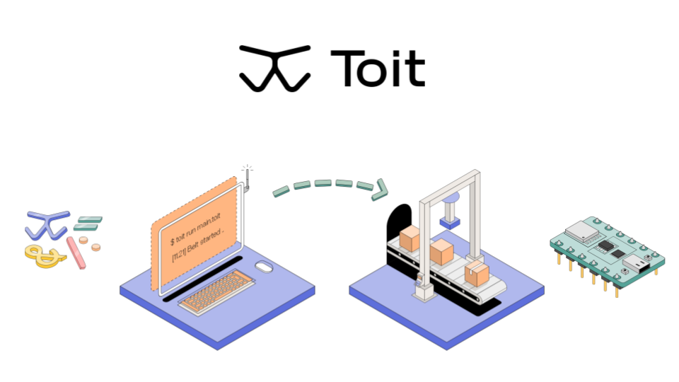
Toit revolutionizes the IoT development process by offering a novel approach that fixes most of the issues inherent to the traditional process. Toit provides you with everything needed for developing an IoT application: firmware, cloud connectivity, a web-based console, and even a new programming language with syntax similar to Python but much faster execution speeds. This article presents some notable features of this all-in-one platform which help IoT developers to build their applications quickly and easily.

Deploy your First Application from Scratch within 15 Minutes

Toit provides a smooth onboarding process for developers who are new to this platform. First-time users need an ESP32 board and a USB cable to flash the firmware. This is a one-time process and future updates for the firmware will be done over the air. After signing up, the web-based console provides almost everything for getting started. Now with the support for flashing from the browser using Web serial, users can start developing even without installing anything on their PCs. This whole process of provisioning your device will take a few minutes and you’ll be up and running.

Toit's Dashboard for Deploying Applications

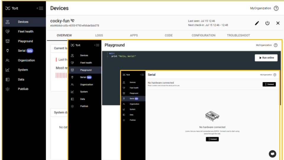
The console provides an inbuilt code editor where you can write, run code on your device and monitor the output with timestamps. This is a great way to quickly try out something and improve your program. Finally, when your program is working as expected, you can deploy it as a long-lived application on your device. If any, the output of the app will be logged and can be seen through the console under the LOGS section.

Efficient Multitasking on a $2 MCU

The multitasking capability of Toit is what makes it stand out from the crowd. On top of that, the isolated memory areas for each application put the icing on the cake. This way, the security of data is taken care of. Multitasking on an MCU with the traditional development process is not impossible but might easily break the whole system even if a small bug comes up. On Toit, it is a light and agile process, so users can easily try out new things without having to worry about bricking the device.

Multitasking with ESP

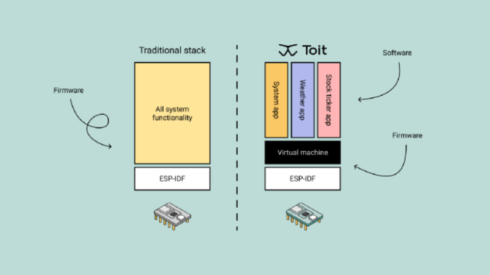
In fact, multiple applications run independently on the device. So, even if one of the apps goes down, the others won’t be affected and the system will keep running normally. Users can just fix the buggy app and re-deploy it as before.

Easy to Use Programming Language and APIs

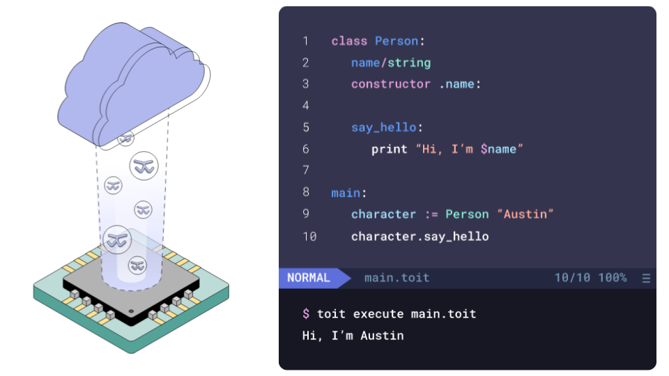
Traditional IoT programming can be done using a lot of programming languages, with C/C++ and MicroPython being the popular ones. The problem here is that writing with low-level language might be painstaking when it comes to microcontrollers. On the other hand, high-level languages like MicroPython make it easy to write code but you’ll have to sacrifice the execution speeds. Toit decided to change everything by creating a new dedicated programming language for IoT. The Toit programming language has syntax similar to Python but is 20 times faster than MicroPython. This new language comes with an automatic memory management system which helps to avoid crashes.

Toit APIs

Toit also provides a publicly available gRPC API allowing users to have complete control over their devices through a client application. As Toit engineers put it, “You are in full control of your devices and everything you can do with the Toit platform, you can do through our API. It is easy to integrate our platform into your products and turn your device fleet fully programmable.” The API definitions and examples are available on their Github repo.

Visual Studio Code Extension to Write and Deploy Apps

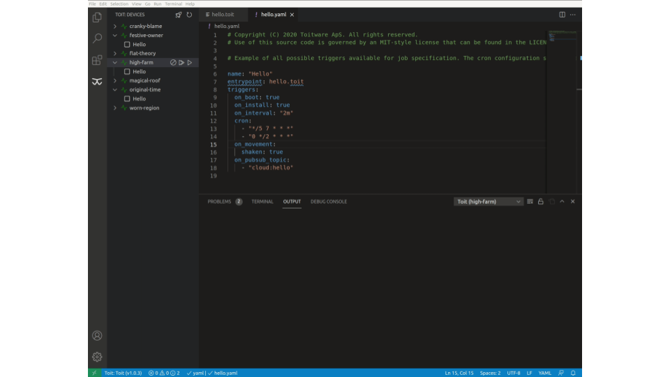
Syntax highlighting has become a necessity nowadays for writing any type of code. With the introduction of a new programming language, Toit released a VS code extension that does much more than just highlighting the code. Users can run code snippets, deploy apps and monitor the output in the inbuilt terminal. The extension also gives an overview of devices and apps running in the sidebar. So altogether, this VS code extension covers all the basic functionalities of the web-based console, while providing a few additional tools for app deployment.

Visual Studio Code Extension

Support for Raspberry Pi is available as a Beta Program

Apart from ESP32, Toit has now released a beta program for working on Raspberry Pi devices as well. Traditionally, Raspberry Pi IoT devices may require as much as 200 MB of code updates. With Toit, the updates are around 50 KB which takes less than 2 seconds to be installed. These updates are small enough to be sent across low-bandwidth cellular connections like NB-IoT or Cat-M1. Developers can also swap their Raspberry Pi with an ESP32 while keeping the same code stack. This way, Toit comes up as a hardware-independent IoT platform.

You can learn more about the Toit IoT platform and its features on their website.

TOP PCB Companies