Single-board computers (SBCs) are becoming more popular as the industry develops and new technologies emerge, such as the Internet of Things (IoT). Therefore, the use of computers and smart technologies in electronics has maximized the growth potential of the global SBC market. Technology advancements, such as artificial intelligence, have made the hardware increasingly sophisticated and compact. Hence, with the increasing popularity of SBCs and their powerful features, many third-party manufacturers have come up with hardware based on the Raspberry Pi form factor.
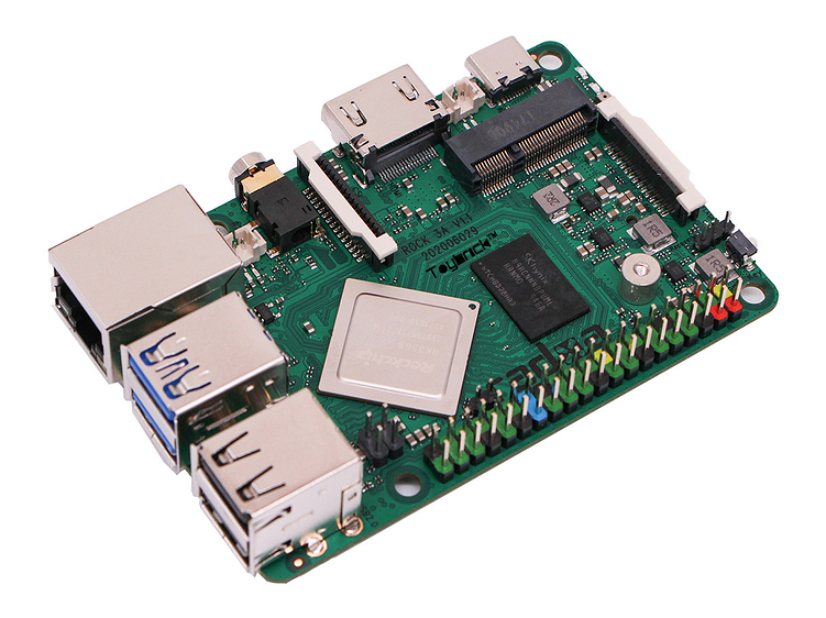
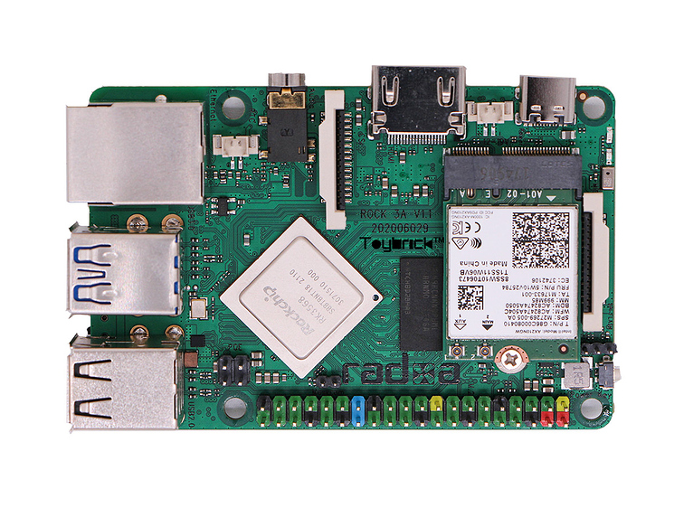
Recently, we have seen the launch of Radxa’s Rock Pi 4 SBC built around the Rockchip RK3599 chip. To continue the emergence of Rockchip-powered development boards, the RK3568-based ROCK 3A is another single-board computer by Radxa. These systems on a chip are very versatile and capable of executing various extensive tasks.
ROCK 3A is a more powerful version of ROCK Pi 4 with a few new interfaces. Hence, as compared to the previous Rockchip RK3399, the new CPU can run at up to 2GHz. Along with this, the GPU is faster than the ARM Mali-T860 MP4, which can run at up to 800-950 MHz. Another peculiarity on the board is SATA support along with two M.2 slots for storage and wireless cards. Thus, the SBC provides the advantage of high-speed reading and writing, large storage space, and a faster transmission rate.
Technical Specifications of ROCK 3A SBC
The onboard RK3568 targets NVR applications and features a quad-core Cortex-A55 CPU, Mali-G52 GPU, and an integrated NPU that delivers 0.8 TOPS of performance. The core works at a frequency of 2GHz, which is also faster than the RK3566 1.8 GHz. Hence, with a 22nm lithography process, it features low power consumption and high performance. Additionally, the ROCK 3A meets the requirements of large-memory applications by offering 8 GB of DDR4 RAM with controller frequency up to 1560MHz. The board also provides QC/PD power support through a new generation QC/PD protocol IC.
To deliver better network scalability, the new hardware includes Gigabit Ethernet(GbE) port with PoE support. Moreover, the board has common I/O interfaces available on a standard SBC. These include MIPI-DSI and CSI interfaces, as well as an HDMI 2.0 port for display interface. With a small form factor of 85 x 54 mm, the SBC also comes with a rich set of physical connectivity through four USB ports and a 40-pin GPIO header compatible with Raspberry Pi.
Like the Rock Pi 4, the Rock 3A SBC includes an M.2 M-key slot with two PCIe 3.0 for NVMe SSD storage. It also features an additional M.2 E-Key slot with WiFi 6 support. The WiFi 6 delivers a lower packet loss and retransmission rate, making the transmission more stable and secure. Furthermore, to facilitate data transmission, the SBC leverages the RK3568’s ability to multiplex SERDES lanes to provide SATA compatibility via the pair of USB 3.0 ports.
According to Radxa, the Rock 3A will support Debian 10 for Rockchip-powered devices, which is managed by Toybrick. However, the board will also support third-party operating systems such as Manjaro Linux, Slackware Arm, etc. The Rock 3A will be available for purchase in August, with pricing ranging from $35 for a 2GB model to $75 for an 8GB model. For more information visit Radxa’s community website.
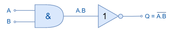
The NAND gate is a logic AND gate with an inverted output. It is a reverse or complement of a AND gate discussed previously. The logic AND gate output logic “HIGH” when all of its inputs are at logic level “HIGH”. Contrary to this, the logic NAND gate outputs logic “LOW” when all of its inputs are at logic level “HIGH” and it will output a logic “HIGH” when any of its inputs goes to the “LOW” state.
Figure 1: Logic NAND Gate
The logic NAND gate can be expressed through logic or Boolean expression of Logical Addition with its inputs inverted. The logic NAND gate Boolean expression is denoted by a dot (.) placed between inputs and an overline. The dot (.) represents a logical multiplication whereas an overline represents a complement (NOT) of inputs. The Boolean expression for a NAND is:
The logic NAND gate is also referred to as Sheffer Stroke Function and is expressed by a vertical bar or arrow between the inputs.
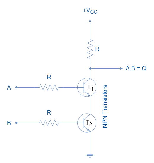
Resistor-Transistor NAND Gate
In the following figure, a basic two-input NAND gate constructed using Resistor-Transistor Logic (RTL) is shown.
Figure 2: The Resistor-Transistor Logic NAND Gate
When both inputs “A” and “B” are “HIGH” then both transistors are in saturated “ON” states and a state “LOW” appears at the output (Q). Turning any of the inputs to logic “LOW” will drive the relative transistor to the “OFF” state and pulls the output (Q) high to VCC.
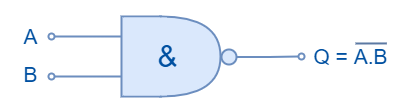
Logic NAND Gate Symbol & Truth Tables
The representation of a NAND logic by a symbol is shown in the following figure. An inversion bubble at the output denotes the inversion of the multiplication.
Figure 3: Logic NAND Gate Symbol
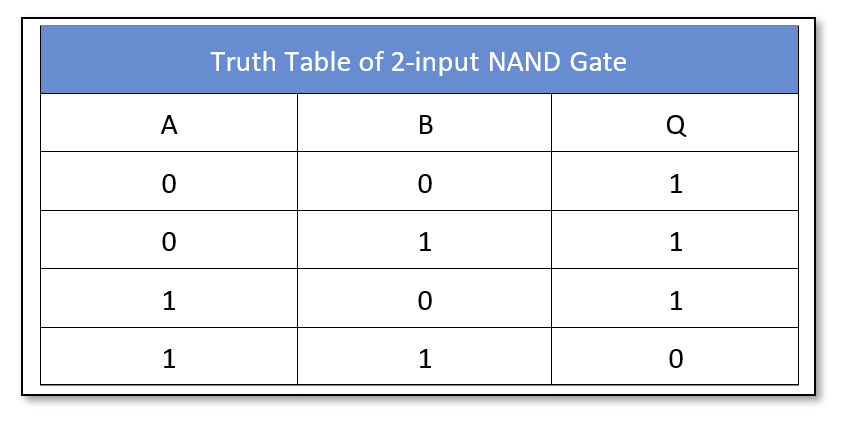
The truth table of a two-input NAND logic gate is shown below:
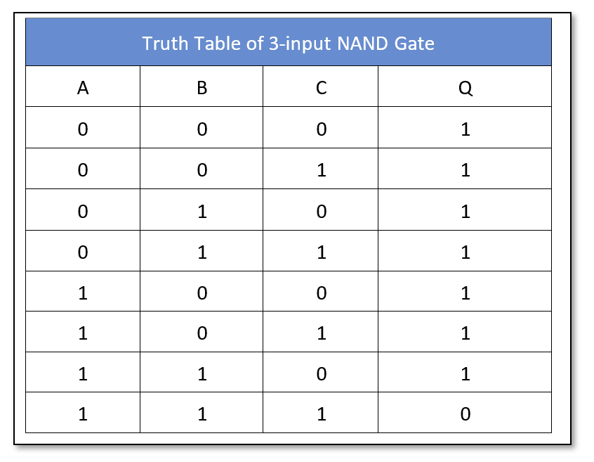
Similarly, the truth table of a three-input NAND logic gate is as follow:
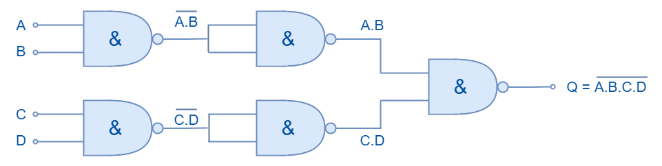
The Boolean expression can be extended to include multiple inputs to obtain a logic NAND operation. The commercially available NAND logic circuits have up to four inputs but the number of inputs can be further extended by cascading the NAND logic circuits. In the following figure, five two-inputs NAND gates are cascaded together to obtain a four-input NAND function.
Figure 4: A 4-input NAND logic constructed by cascading multiple NAND gates
The Boolean expression for this cascaded circuit can be written as:
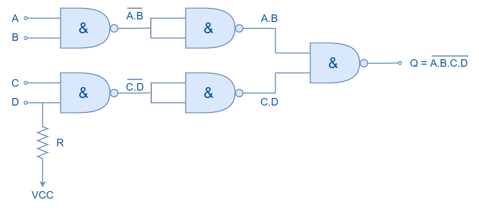
Odd Number of Inputs
The NAND logic circuit having an odd number of inputs can be constructed by driving the unused input to logic “HIGH”. This will ensure that another input(s) of the NAND logic gate is truly reflected in the output. It is explained in the following diagram where unused input is pulled high using a pull-up resistor.
Figure 5: The NAND logic having an odd number of inputs
Universal Gate
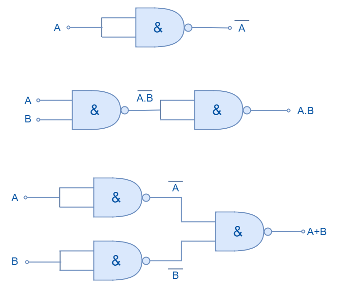
The logic NAND gate is described as a universal gate because it can be used to form the other logics i.e. AND, OR, NOT, Exclusive OR, Exclusive NOR, and NOR, etc. It is the most common and widely used logic gate because of its Universal Gating capability. The examples of forming the AND, OR, and NOT logic by using NAND gates are shown in the following figure.
Figure 6: Forming NOT, OR, and AND gates using NAND gates
Commercially Available NAND Gates
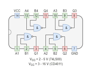
The NAND logic gates are available in both TTL and CMOS logic families. The most commonly used NAND logic packages are:
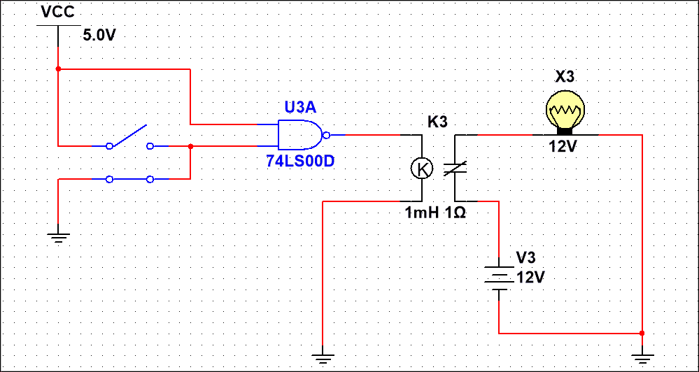
In the following figure, a NAND gate is used to drive a 12V relay to switch on the lamp using NI Multisim. The NAND gate (74LS00) turns off the relay when all of the inputs are connected to VCC. The relay thus turns off the lamp through an external circuit of 12V. When one of the inputs is connected to Ground, NAND logic goes “ON” turning the relay and lamp to “ON” state.
Figure 8: A Multisim circuit showing NAND logic to control an external circuit
Conclusion
The output of the NAND logic is “LOW” when all of the inputs are in logic “HIGH” states.
Any of the inputs in the logic “LOW” state will drive NAND logic to the “ON” state.
The NAND gate is sometimes referred to as Sheffer Stroke Function and is denoted by a bar between the inputs.
The NAND logic gates can be constructed using Resistor-Transistor Logic (RTL) but are seldom used because of the propagation delay and power consumption.
The NAND gate is termed a Universal Gate because of its capability to form any other logic using only NAND gates.
The NAND logic gates commercially available have up to eight NAND logic inputs. However, inputs can be extended by using cascaded NAND logic gates.
The NAND logic circuit having an odd number of inputs can be constructed by using a pull-up resistor on the unused pin.
An external circuit can be controlled by NAND logic with the use of a magnetic relay.
Surface Mount Technology was developed in the 1960s. During the 1970s and 1980s a revolution in the automation industry was begun, which raised the demand for Surface Mount Technology Components for a better assembly process. Before Surface Mount Technology, electronic components came with wire leads that were not ideal for complex devices. Moreover, such components with wire leads, now commonly known as through-hole components, were making the PCB assembly process significantly slow and costly. These problems were resolved by Surface Mount Technology (SMT), which has opened the door for the invention of complex electronics like mobile phones, laptops, medical products, industrial controls and sensors, and many more.
Surface Mounted Technology or “SMT” is used within the great majority of commercial electronics nowadays. The complex nature of SMT benefitted most applications of commercial electronics with the need to fit into very small spaces. To achieve this, components must be mounted directly onto the PCB surface as opposed to through-hole wire leads inserted into the board.
To say SMT was an important invention is an understatement. Electronic devices we have now would be much larger than they are. In fact, it’s safe to say that it’s a widely popular choice in today’s electronics. The reasons are many, including cost, size, simplicity of assembly and the amount of functionality demanded within a small volume. It’s these vital advantages that have seen SMT devices dominate the market. Here’s a rundown of some of the advantages afforded to surface-mounted technology devices.
Advantages of Surface Mounted Technology
SMT allows for automated production and soldering and makes the whole process quick and simple. This results in considerable savings in time and money and allows for a lot more consistency in output..
Fewer holes are required to be drilled into circuit boards; consequently, this makes the PCB more robust and cheaper.
Costs of SM components are much lower than through-hole components.
Both sides of the circuit board can have SMT parts on them, offering much more usable space. Moreover, SMT components are much smaller, which in turn saves valuable, maybe crucial space.
SMT components offer much better performance under vibration and dropping or shaking, as they are much lighter in weight; The SMT component can weigh as little as one-tenth of their common through-hole equivalents.
Unlike through-hole components, small errors in the placement of components are corrected automatically since the surface tension of molten solder pulls SMT components into alignment with solder pads. A well-designed PCB will optimize this.
PCBs made from SMT components generally have lower resistance and inductance. This can be crucial for better high-frequency performance and to filter out unwanted RF signal effects.
SMT components offer a smaller radiation loop area, hence provide better EMC (Electromagnetic Compatibility) performance.
As with everything in life, while something may have its advantages, it will usually have a few disadvantages too. These include:
High power output or physically large parts aren’t suitable. You must use through-hole construction for that and other design requirements.
Manual repair of surface-mounted technology can be tricky due to the significantly smaller size of SMT component joints. You will need well-trained operators and sophisticated equipment in order to carry out efficient repair and rework.
SMT component joints can be less physically robust than through-hole components. This is due to the physically smaller joints with less solder. The void formation can easily be missed during inspection of the assembly due to the smaller dimensions, contributing towards poor thermal and mechanical performance. Skillful design and layout of the PCB can help mitigate this.
Surface Mounted Technology isn’t suitable for components that endure frequent connecting and subsequent disconnecting. The mechanical strain on unsupported SMT components has a far worse effect than it does with through-hole components (which are by default, anchored into the PCB)
SMT components are not suitable for applications that require the whole design to be sturdier against external forces. Through-hole technology provides more protection against environmental stress, and it has retained more application in the military and aerospace industry because of this.
Scope of Application:
To conclude, SMT components are ideal when it comes to applications that are sensitive to processor speed, where resistance and inductance of circuits are important ( for example RF communication and high-speed digital processing). For high-frequency applications, these are pivotal advantages over rather insignificant disadvantages. In higher current or harsh vibration environments, the advantages of SMT are outweighed by the vulnerability, and through-hole technology would be better. You, therefore, need to use your expertise while considering the pros and cons of Surface Mount Components with their through-hole counterparts for each application. It is also vital not to overlook the optimization of your PCB design while making your ideal selection.
Contact Advanced Rework Technology Today
Training is available to help comply with best practices in the design and assembly of SMT products. We recommend that your designers are qualified for to “Advanced Certified Interconnect Designer (CID+)” status. We recommend that your production staff are trained and regularly re-certified for some of the several IPC courses applicable to the circuit board and cable harness production. This will ensure consistent output quality and less rework, thereby reducing costs and lowering product reject rates in service. Ask us for a free consultation on how we can help. Contact A.R.T today or give us a call and speak to one of our team on 01245 237 083.
Fibocom, a global leading provider of IoT (Internet of Things) wireless solutions and wireless communication modules, announced that the Fibocom 5G module series FM150/FG150 has received the 2021 IoT Evolution Product of the Year Award presented by IoT Evolution World, a leading magazine and website covering IoT technologies.
Based on the Qualcomm SDX55 chipset platform, Fibocom’s 5G module series FM150/FG150 is one of the world’s firstly launched 5G module series in 2019. The modules support both 5G SA and NSA network architectures, which brings greater network capacity, faster data transmission speed, and ultra-low latency to the verticals. The Fibocom 5G module series FM150/FG150 has been selected by 500+ customers and industry partners, deployed in 100+ terminal devices and used in 20+ vertical industries.
The award honors the best and most innovative products as well as solutions powering the Internet of Things. Recipients of this year including Verizon Connect, Digi International, FairCom, Very, Palo Alto Networks, VMware, etc.
“We are honored that our FM150/FG150 5G module series has won IoT Evolution’s Industrial IoT Product of the Year Award”, said the director of Fibocom product management dept. “As a leading provider of IoT solutions and wireless modules, Fibocom look forward to bring 5G connectivity to accelerate digital transformation around the world.”
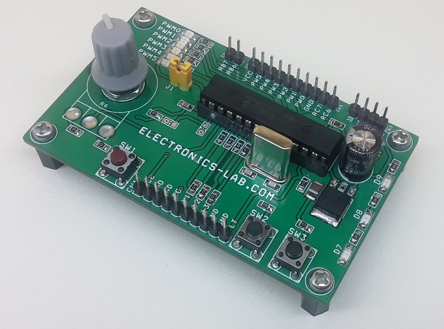
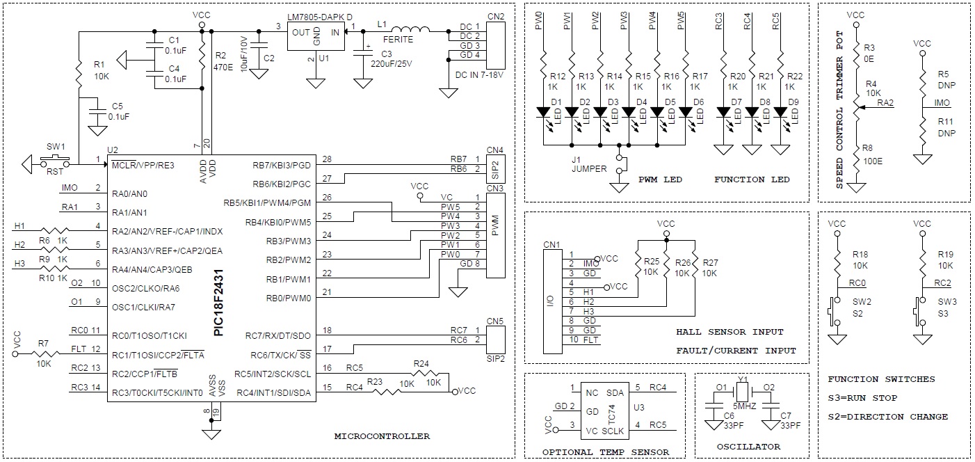
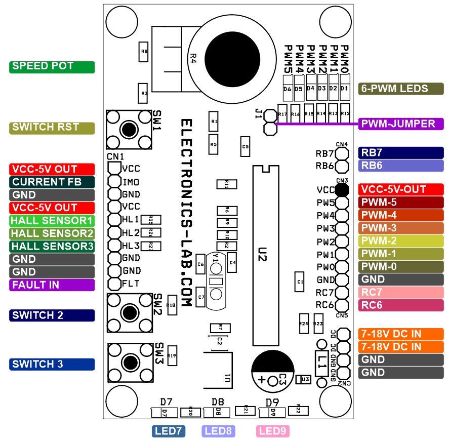
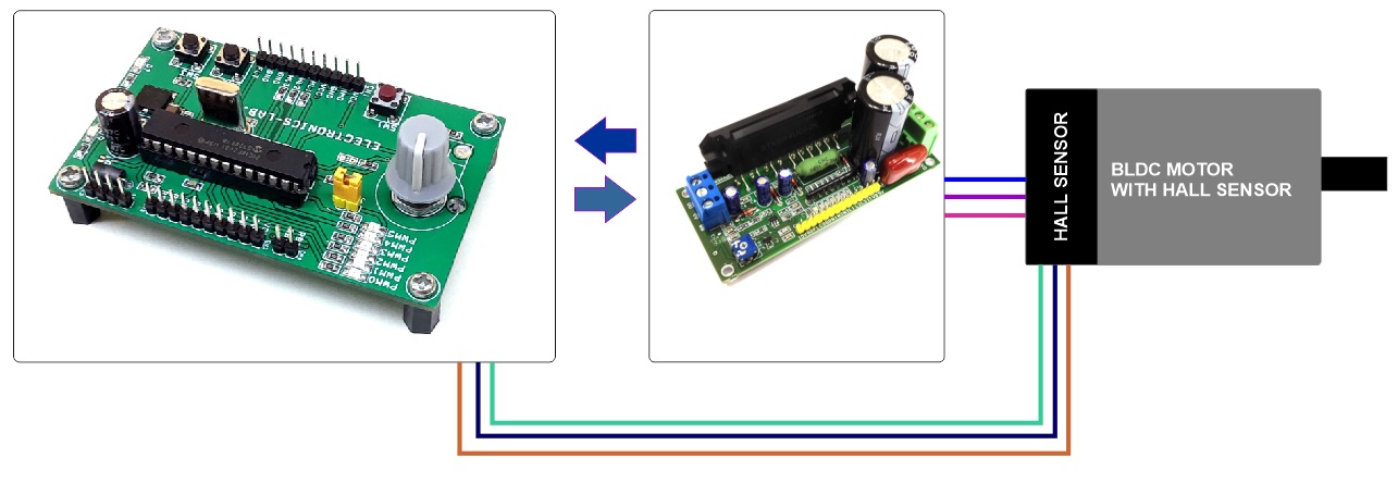
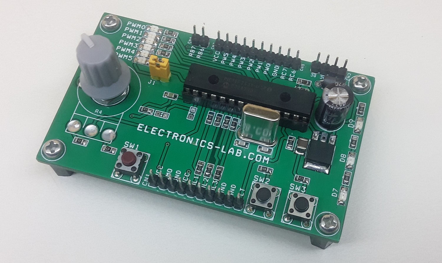
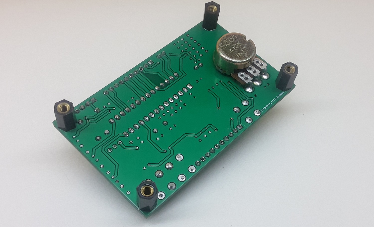
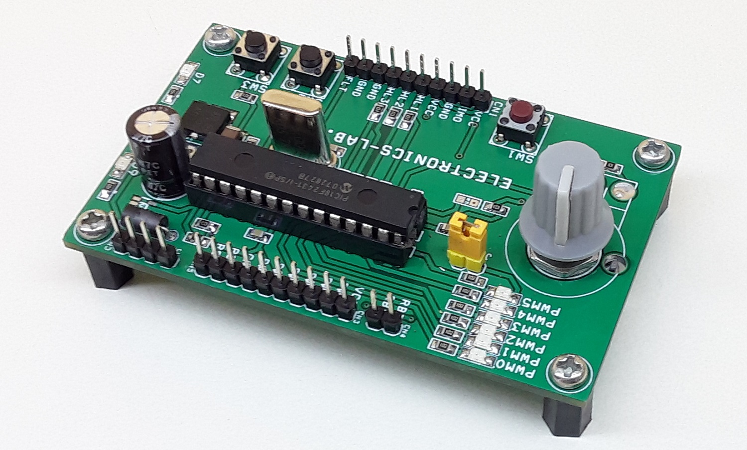
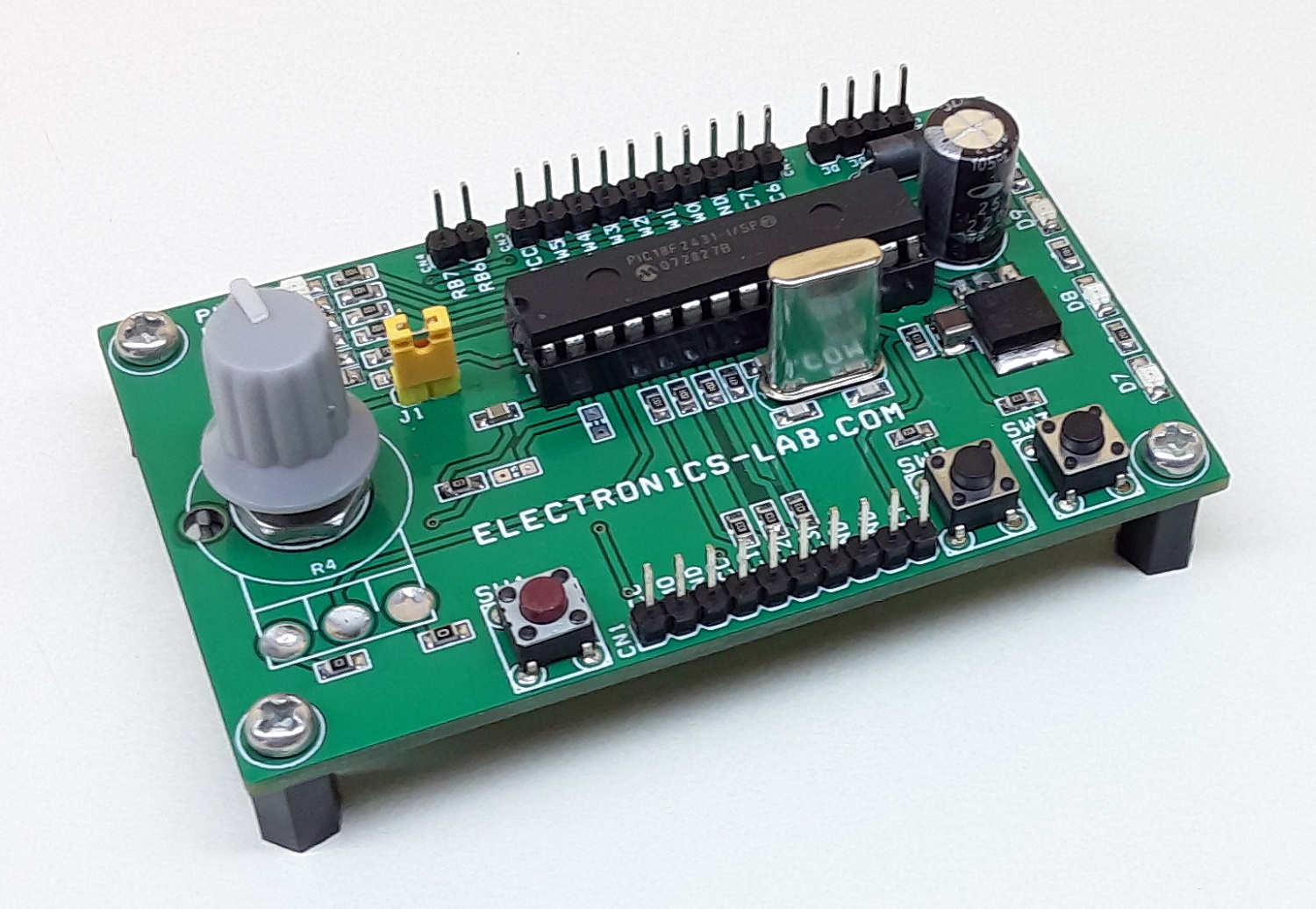
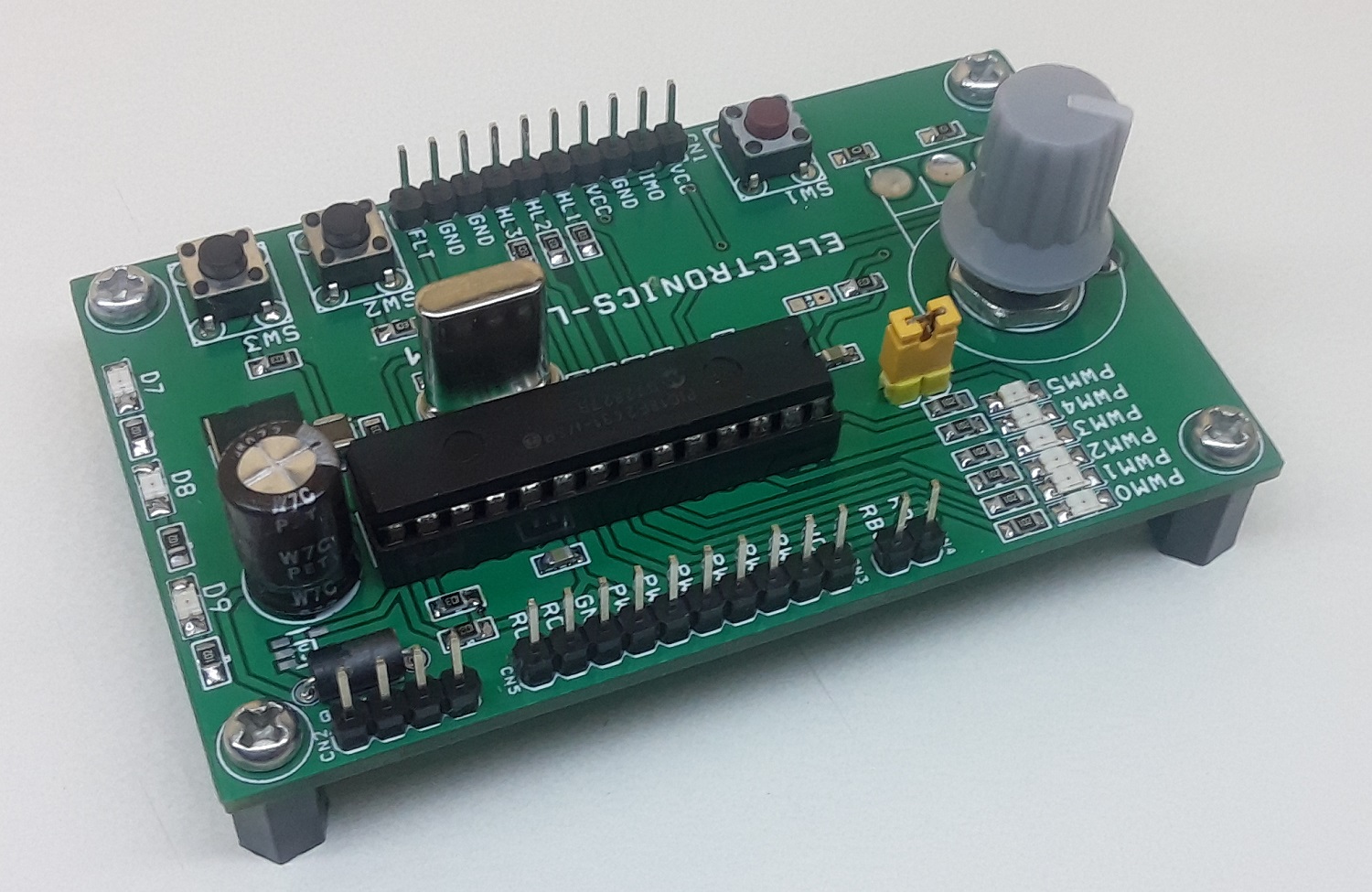
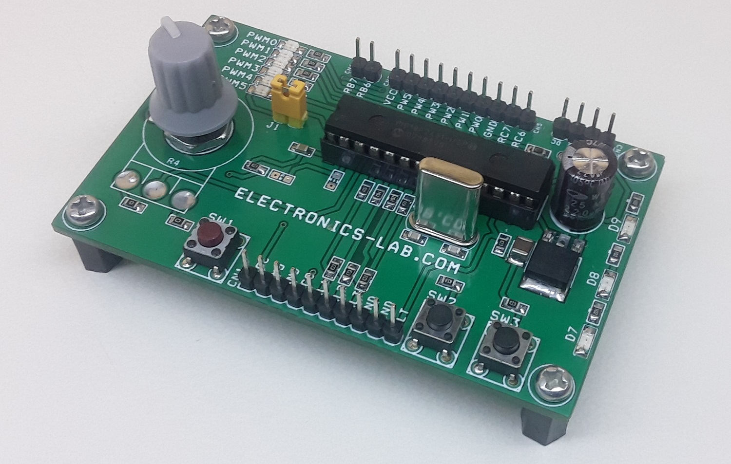
The project described here is a pre-driver for brushless motors with a hall sensor. The board incorporates many features like current monitor, fault, speed control, direction control motor start/stop using tactile switches, various function LEDs, 6 PWM LEDs. By combining it with a hybrid IC or IPM module large size high voltage and high current motor can be driven. The project is compatible with the Microchip PICDEM MCLV motor development board, HEX firmware of the MCLV board can directly work with this board. This board is mainly targeted to control brushless DC (BLDC) motors in hall sensor operations. The board supports a free, ready-to-use MC-GUI (Motor Control – Graphical User Interface) from Microchip. Using the MC-GUI, the user can easily set and/or change motor parameters. This greatly helps the user in developing customized drive solutions. Temperature sensor chip U3 is optional so do not populate. The fault pin has to be high for normal operation, bring it to GND to disable the operations. This pin can be used as over current input from ITRIP pin or an over-current comparator of the IPM module. Overcurrent can be monitored using the IMO (RA0) pin of IC in the range 0 to 3V. PWM Frequency default 20Khz with example HEX code. Hex code is available as a download.
This flexible and low-cost board can be configured in different ways to use with Microchip’s specialized motor control microcontrollers. This low-cost board has the facility to use either the PIC18F2331/2431, this hardware can be used to drive AC motor, Brush DC motor, Brushless DC motor, and solenoid. Various inputs and outputs pins are available, microcontroller has dedicated 8 power module PWM, Motion feedback Optical encoder or hall sensors, ADC to connect with a potentiometer, current feed, voltage feedback, and FOC signals. Project is compatible with microchip PICDEM MCLV board, HEX firmware of MCLV board directly can work with this board. This board is mainly targeted to control brushless DC (BLDC) motors in hall sensor operations.
Note 1: This board is compatible with PICDEM MC LV (Only Pre-Driver). Please refer to the user guide of PIC DEM MCLV before assemble and use this board.
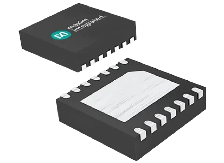
Maxim Integrated MAX25302A/B 2A Automotive LDO Linear Regulators are 1.7V–5.5V VIN, low-noise linear regulators. The regulators deliver up to 2A of output current with only 5.1μVRMS of output noise from 10Hz to 100kHz. They maintain ±1% output accuracy over a wide input voltage range, requiring only 100mV of input-to-output headroom at full load. The 1.3mA no-load supply current is independent of dropout voltage.
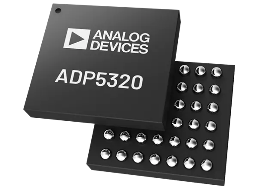
Analog Devices Inc. ADP5320 Power Management Unit (PMU) is designed to meet the demanding performance and board space requirements for wearable applications. This PMU combines nine digitally adjustable regulators, a fuel gauge, a 12-bit ADC, 2KB of OTP memory, and anticounterfeit logic in a 42-ball. The regulators include 2x buck-boost, 1x buck regulator, 5x Low Dropout (LDO) regulators, and one low input LDO. This ADP5320 PMU operates from a 1.8V to 5.5V input supply voltage range that enables the device for use with multiple types of battery inputs. The PMU features a power-good monitor, watchdog power hard reset, and I2C interface with interrupt warning.
The ADP5320 PMU fuel gauge includes a precision 16-bit coulomb counter that integrates battery current flowing through the device. A 12-bit ADC is included to monitor battery voltage, output supply voltages, and junction temperature. The ADP5320 PMU buck-boost regulators are high efficiency, step up and step down regulators. This PMU operates from -10°C to 70°C temperature range. Typical applications include wearable medical applications, IoT applications, disposable sensor devices, and battery-powered devices.
Features
1.8V to 5.5V wide input supply voltage range
5.1μA standby mode low quiescent current, including UVLO
16-bit coulomb counter fuel gauge with integrated high-side current sensing resistor
12-bit ADC to monitor battery voltage, output voltages, and junction temperature
Channels 1 and Channel 2:
150mA low power buck-boost regulator
Selective buck, boost, or buck-boost operation
Selective hysteresis or Pulse-Width Modulation (PWM) mode
50kHz to 225kHz selective PWM frequency
2x programmable GPIOs for clock synchronization or fast stop switching input
Channel 3:
150mA low power buck regulator
Channel 4 through Channel 6, and Channel 8:
50mA low noise LDO and 1.65V to 5.5V input supply voltage range
Channel 7:
50mA sink current LDO
Channel 9:
50mA, low noise LDO, and 1V to 1.9V input supply voltage range
I2C interface with interrupt warning
2KB OTP memory
Power-good monitor and watchdog power hard reset
UVLO, peak current-limit protection, and TSD protection
Integrated anticounterfeit logic module
42-ball, 0.40mm pitch, and 2.880mm x 2.980mm WLCSP
-10°C to 70°C operating junction temperature range
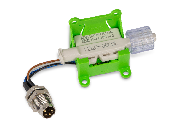
The LD20 single-use liquid flow sensor series from Sensirion, the expert in flow and environmental sensor technology, is suitable for fast, precise and reliable measurements of the lowest flow rates in biomedical applications. The evaluation kit for the LD20-0600L version is now also available from distributors. The sensor manufacturer thus provides its customers with the sensor quickly and easily for initial evaluations and proof-of-concept prototype tests in small quantities.
The LD20-0600L liquid flow sensor is based on Sensirion’s proven CMOSens® Technology and optimizes costs by simplifying the design without sacrificing easy fluidic, electrical and mechanical connections. Luer lock fittings ensure safe and secure integration into the fluidic line. The straight and unobstructed flow channel design has no moving parts. Medical-grade wetted materials provide outstanding chemical resistance and excellent media compatibility. While it can provide bidirectional measurement of ultra-low flow rates up to 20 ml/h, the sensor can also be used to detect common failure modes such as occlusion, air in line or free flow with unprecedented speed and sensitivity.
Features
20ml/h full-scale flow rate for water-based liquids
Bidirectional measurement and real-time failure detection
High sensitivity for detection of occlusions and air-in-line events
Media isolation so the sensor chip has no contact with valuable medications or body fluids
Inert, medical-grade wetted materials
<50ms response time
Low power consumption
Fully calibrated, linearized, and temperature compensated digital I2C signal from a single chip
The logic NOT gate always returns a not (opposite) of the input signal. It is the simplest and most basic form of a logic gate having only one input and one output. The logic NOT gate is also termed as Inverting Buffer or an Inverter because of its inverting response.
A logic level of “LOW” at the input of a logic NOT gate will be returned as “HIGH” at its output and a logic “HIGH” input will be inverted to “LOW” at the output. In other words, a logic NOT gate complements the input signal at its output.
Because of its complementing response, it is called a logic NOT gate. When the input will be “HIGH” its output will NOT be “HIGH” and, similarly, when its input is “LOW” then its output will NOT be “LOW”.
The logic NOT Boolean expression or logic can be expressed as:
Q= A’
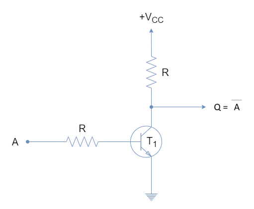
Resistor – Transistor NOT Gate
The logic NOT gate can be constructed using a simple Resistor – Transistor logic as shown in the following figure:
Figure 1: The Resistor-Transistor Logic “NOT” Gate
The transistor switches between saturated “ON” and “OFF” states depending upon the signal present at its base. At logic “LOW”, the transistor will be in “OFF” state and the logic “HIGH” appears at the output. Whereas, a logic “HIGH” at the input of the base will switch the transistor to an “ON” state and connects the output to the ground or zero potential. Hence, a logic “LOW” appears at the input. It is obvious that the circuit is performing as a function of inverter or logic NOT gate.
Logic NOT Gate Symbol & Truth Table
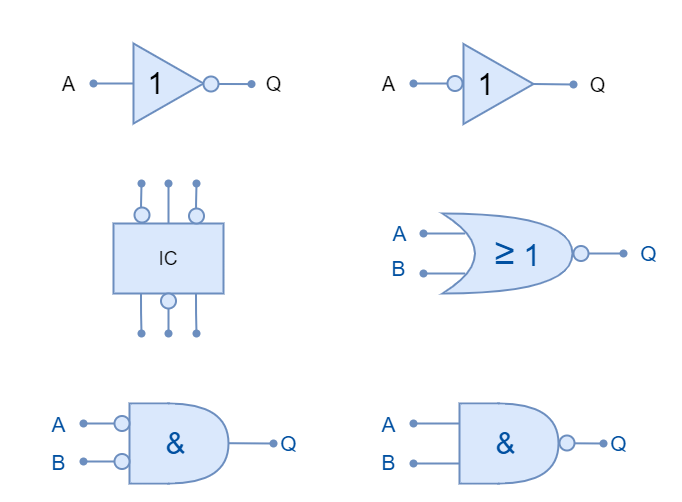
The logic NOT gate symbol has a triangular shape and points towards the output with a circle. The circle denotes the inversion and is called “Inversion Bubble”. The base or flat side of the triangle has the input connected to it. The symbol of a logic NOT gate is shown below:
Figure 2: Logic “NOT” Gate Symbol
The simple truth table of a simple NOT gate is:
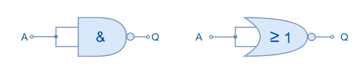
The “Inversion Bubble” is also used in other logic gates to denote the logic inversion. Such as the “Inversion Bubble” at the output of AND and OR gates will represent a logic of NAND and NOR, respectively.
The “Inversion Bubble” can also be used at the inputs to represents an active-low signal which leads to a logic “HIGH” even though the input level is at “LOW”. It is simply an inversion at the input of a logic gate. The active-low signals are represented by circles at the pins of an IC’s pinout diagram.
The following set of figures show a number of variations of logic inversions.
Figure 3: Logic Gates with Inversion Bubbles
Commercially Available NOT Gates
The logic NOT gate is available in both TTL and CMOS logic families. Normally 4 or 6 NOT gates are packed within a single commercial IC package. The most commonly used NOT logic packages are:
CMOS based OR Gate IC Package
CD4009 Hex Inverter
CD4069 Hex Inverter
TTL based OR Gate IC Package
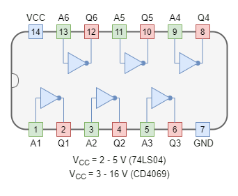
74LS04 Hex inverter
74LS1004 Hex Inverter
Figure 4: 74LS04 Package having hex “NOT” gates
Example of OR Logic
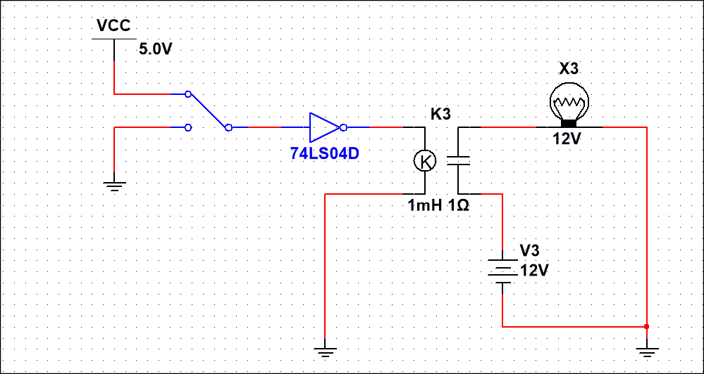
In the following figure, a NOT gate is used to drive a 12V relay to switch on the lamp using NI Multisim. The NOT gate (74LS04) energizes the relay when a “LOW” logic input is applied. The relay thus turns on the lamp through an external circuit of 12V. When the input is at the logic “HIGH” level, the 74LS04 will invert the “HIGH” to “LOW” and switch off the relay to turn off the lamp.
Figure 5: A Multisim circuit showing “NOT” logic to control an external circuit
NAND and NOR Gate Equivalents
An inversion logic or NOT logic can also be achieved by using NAND or NOR gate. A simple 2-input NAND or NOR gate can be used for this purpose as shown below figure. The inputs of NAND or NOR gate are shorted to make a common input and outputs of NAND and NOR gates are dependent on this common input which will always be inverted.
Figure 6: A logic “NOT” equivalents using NAND and NOR gates
Schmitt Inverter/ Hex Inverter
As discussed above, a logic NOT gate can be constructed using a transistor. However, transistors take time to switch between saturated “OFF” & “ON” states. The switching is accompanied by some time delay in transistors and is not instant. Moreover, the transistor has the dominant characteristic of amplification and which may lead to its operation in amplification mode. In linear amplification operation, a small change in the input leads to a significant change in its output which can also cause to switch between “OFF” & “ON” states abruptly. A Schmitt Inverter or Hex Inverter can be used to avoid these problems.
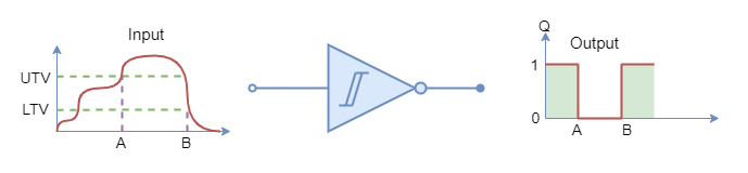
As discussed in the previous article(s), in TTL family 2 to 5V is considered as logic “HIGH” and 0 to 0.8V as logic “LOW”. The voltage level of 0.8 and 2V can be set as Lower Threshold Voltage (LTV) and Upper Threshold Voltage (UTV), respectively. The Schmitt Inverter operates on these LTV and UTV limits and changes its state instantly. Whenever the input voltage level rises above UTV i.e. 2V then Schmitt Inverter output changes to logic “LOW” (obviously, it is an inverter), and as soon as input voltage drops below LTV i.e. 0.8V then its output changes to logic “HIGH”. It keeps the previous state during the transition period and switches state instantly upon reaching threshold voltages. It can be said to have a Hysteresis built into the Schmitt Inverter.
Figure 7: A Schmitt Inverter symbol and working
Schmitt NOT Gate Oscillator
A very useful and common application of Schmitt Inverters is found in oscillators.
Square-Wave Oscillator
A simple Schmitt RC oscillator is shown in the following figure.
Figure 8: A RC Schmitt Inverter Oscillator
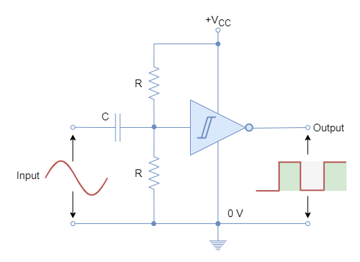
Initially, the capacitor is discharged and zero voltage is present at the input of Schmitt Inverter which is equivalent to logic “LOW”. Resultantly, a logic level of “HIGH” appears at the output due to inversion and the capacitor starts charging through the feedback resistor (R). The Schmitt Inverter changes its output from “HIGH” to “LOW” as soon as the capacitor charges to the upper threshold limit (UTL). The capacitor then starts to discharge through the feedback resistor (R) and Schmitt Inverter changes state from “LOW” to “HIGH” as soon as capacitor voltage hits lower threshold limit (LTV). The switching of the states continues producing a square wave at the output.
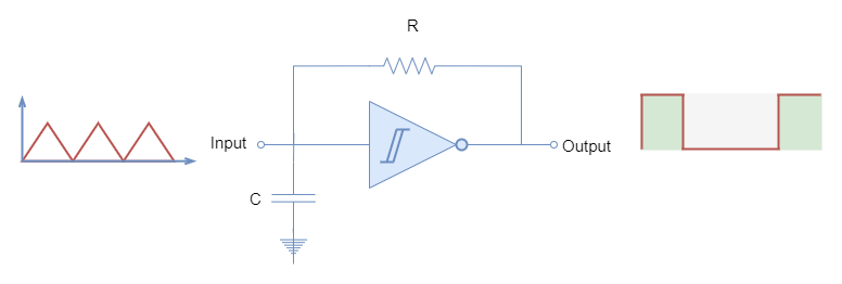
Sine-to-Square Wave Converter
The following Schmitt Inverter circuit converts the Sine-Wave to a Square-Wave. The voltage divider at the input of the Schmitt Inverter sets the quiescent point. Whereas, the capacitor at the input acts as a decoupling capacitor to block the DC component and allows Sine-Wave to pass through it. The Sine-Wave magnitude passes through UTV & LTV of Schmitt Inverter and the output of Schmitt Inverter switches between “ON” and “OFF” states. A Square-Wave appears at the output having a switching frequency equal to that of the Sine-Wave.
Figure 9: A Sine t0 Square Wave converter using Schmitt Inverter
Conclusion
The NOT gate has a logic of inverter and an inverted logic of input appears at the output.
A logic NOT gate results in a logic “LOW” when input logic is “HIGH” and in a logic “HIGH” when input logic is “LOW”.
The NOT Gate is also called an Inverter Buffer or simply Inverter.
It is symbolized by a triangle with a circle at its output terminal. The circle is termed as “Inversion Bubble” and is commonly used at the terminals to denote an inversion or active-low input.
The logic NOT can also be achieved by using NAND or NOR gate.
The logic NOT can be constructed using Resistor – Transistor Logic but TTL, CMOS & Schmitt Inverters have logic NOT gates commercially available in IC packages.
The Schmitt Inverter or Hex Inverter overcomes the issues of switching delays due to transistors-based logic circuits.
The Schmitt Inverters are commonly used in oscillators and signal converters.
Taoglas’ Accura UWC.40 is a tiny indoor centimeter-level positioning antenna for European and United States applications
Taoglas’ Accura UWC.40 is a tiny indoor centimeter-level positioning antenna with high efficiencies across the pulsed UWB communications bands. With dimensions of only 6 mm x 7 mm x 3 mm, the UWC.40 is a very small antenna that is reliable and powerful, with more than 80% efficiencies across most of the UWB bandwidth.