Open Source DC-SCM Compatible BMC Hardware Platform

The popularity of Open source software has brought about impressive successes in the SaaS space, where useful products can be rapidly created from open source components. We see cloud providers and users looking at building their servers using open source hardware as well. This is where Antmicro steps in. Antmicro has been supporting companies like Google, in creating useful server-facing open source hardware such as Scalenode or ARVSOM. One of these projects with Google is an open source hardware FPGA-based Baseboard Management Controller (BMC) platform compliant with the new DC-SCM specification to help increase the security, configurability and flexibility of server management and monitoring infrastructure, which has been adopted by the LibreBMC workgroup as the base hardware platform.

Developed by the Open Compute Project, the Datacenter-ready Secure Control Module (DC-SCM) is designed to move common server management, security and control features from a typical motherboard into a module designed in one of the two form factors featured in the specification (Horizontal or Vertical), which can be used across various datacenter platforms. This spec will enable leading players in the industry share costs, risks and increase reuse. Speaking about the benefit of the DC-SCM, the company says:

“Coupled with a fully open source implementation based on our open source FPGA-based modules, it has a chance to redefine the way board management is done. Basing the module on popular, inexpensive FPGA platforms will not only allow for more configurability and a tighter integration between hardware and software, but also tap into the momentum behind the broader open source hardware community via groups like CHIPS Alliance, OpenPOWER and RISC-V.”

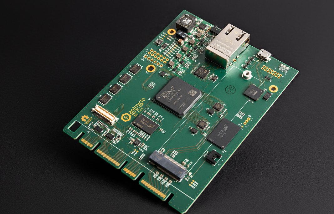
The company developed two implementations of the DC-SCM-compatible BMC, with both designs meeting the Open Compute Project specification for a Horizontal Form Factor 90×120 mm DC-SCM. The BMC is designed to monitor the system, prevent and mitigate failures, and act as an external watchdog. The module enables a feature-packed Secure Control Interface for communication with the host platform, including:

  • PCI Express
  • USB
  • QSPI
  • SGPIO
  • NCSI
  • multiple I2C, I3C and UART channels.

What is unique about the BMC is merging DC-SCM’s central Baseband Management Controller and programmable SCM CPLD block into one powerful FPGA. This solution enables remote updates of DC-SCM peripherals, and most notably, placing OpenPOWER or RISC-V IP cores as central processing units of the module. One of the designs is based on the Xilinx Artix-7 FPGA, and the other one features a Lattice ECP5 FPGA, which are both low-cost and open source friendly FPGAs supported by the open source SymbiFlow FPGA toolchain project which the company is involved with. The FPGA features 512MB of DDR3 memory, 16GB of eMMC flash, and also a dedicated Gigabit-Ethernet interface. For security of the Datacenter Control Module, external cryptographic modules: Root of Trust (RoT) and Trusted Platform Module (TPM) can be connected.

The DC-SCM boards which is being adopted by the LibreBMC Workgroup, operates under the umbrella of the OpenPOWER Foundation. The LibreBMC workgroup, in conjunction with IBM, Google and Antmicro, among others, are involved in creating FPGA gateware and software needed to make the hardware fully operational in real-world server solutions. About future plans for the BMC, the company says:

“Variants involving both Linux (in its default open source server-oriented distribution, OpenBMC) and Zephyr RTOS, as well as with both POWER and RISC-V cores are planned and thanks to the flexibility of FPGA all of those options will be just one gateware update away. Of course, both the gateware and software will be open source as well.”

For more information, visit Antmicro’s blog.
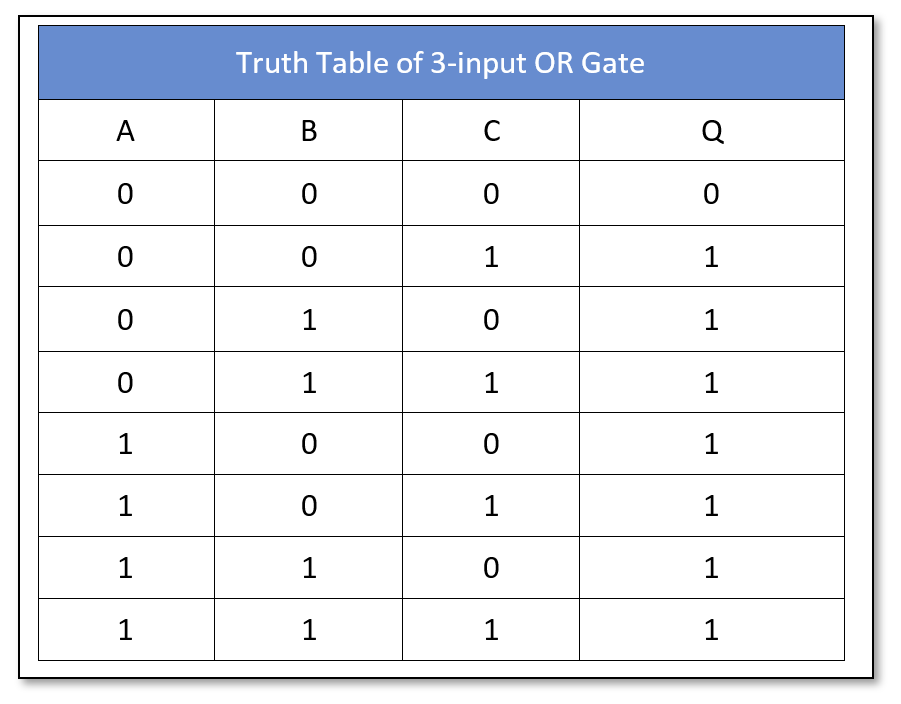
600W – 230VAC – High Voltage DC Motor Speed Controller – Heater Controller – Lamp/LED Dimmer

This is a very powerful DC Motor speed controller for DC motors up to 330V DC and current up to 2A. Basically, the project is a high voltage PWM source with adjustable frequency and adjustable PWM duty cycle range 0 to 99%.  The board has been designed considering many applications and the circuit can be used as a heater controller, DC Motor speed controller, LED dimmer, Lamp dimmer, and High voltage PWM driver. The circuit can handle load up to 600W (330V DC @ 2A). The operating input supply is 100V AC to 250V AC or 100V to 330V DC. It is important to provide the input supply as per the operating power supply of the load. Trimmer pot PR1 is provided to adjust the frequency, and P1 to adjust the PWM duty cycle.

Connector CN2 is used for AC or DC load voltage supply, F1 Fuse for protection, R1 NTC to control inrush-current, C2 and C6 for EMI noise, C7 and C8 DC Bus filter capacitor for load supply, R12 Current sense resistor for overcurrent protection feedback circuit (CSC), R3 Temperature monitor (NTC) divide resistor for temperature feedback output, C3, C4 logic supply filter capacitors, CN1, R2 pull up resistor for Fault (VFO), SG3525 PWM Generator, Q1 BC847 to inverse the PWM, D1 power LED, U1 5V regulator.

FBA42060 – Intelligent Power Module (IPM)

The project is built using the FBA42060 IPM chip. This IPM chip is made for power factor correction, and consists of an inbuilt bridge rectifier, diode for back-EMF protection for inductive loads, IGBT to drive the loads, and IGBT gate driver and on chip NTC temperature monitor.

Precautions for High Voltage

This project should be installed, adjusted, and assembled by a qualified person familiar with the construction and operation of the project and the lethal voltage involved. Failure to observe this precaution could result in severe injury.

The project can be used in a standalone mode or with a microcontroller interface.

Standalone Mode

Solder all components from PWM block, driver chip block, and regulator LM7805. The circuit requires 15V DC to driver logic supply, and Load supply as per operating supply of load.

  • Logic Supply 15V DC (Connector CN1 Pin1 and Pin 2)
  • Load Supply CN2, 100V – 250V AC or 100V to 330V DC (load Supply will depend on Operating Voltage of Load)
  • Fault Output is available at PIN 4 of CN1, normally this pin is high 5V TTL, goes low when fault condition arrives
  • Frequency Approx. 20 Khz When Trimmer Pot is in Middle (Range 3Khz to 60Khz)
  • Duty Cycle 0 to 99% (Speed Control/Dimmer), P1 Trimmer Potentiometer provided to adjust the duty cycle
  • CN3 to connect the Load
  • LED D1, Power LED
  • PCB Jumper J1 Closed
  • PCB Jumper J2 Open
  • Soft Start Feature active
  • Inbuilt Overcurrent circuit is active

Microcontroller Interface

Do not solder components from PWM blocks, use only drive chip block, use current feedback circuit, if current output required.

  • Logic Supply 15V DC (Connector CN1 Pin 1 and Pin2)
  • CN1 Pin 3 PWM Input Duty Cycle 0 to 100%
  • CN1 Pin 3 VFO, Fault Output, normally this pin is High-5V TTL, goes low when a fault condition occurs
  • CN1 Pin 4 VT – Over temperature feedback, refer to the datasheet of the chip for more information
  • CN1 Pin 5 CO – Current Feedback Optional
  • CN1 Pin 6 – GND
  • CN1 Pin 7- 5V DC Output

Testing and using this project

It is important to use an isolated logic supply of 15V. It is important to take proper precautions to handle and use this project, especially while adjusting the PWM and frequency since lethal high voltage DC is used. Don’t touch the PCB tracks and pads until and unless the DC bus capacitors are fully discharged, high voltage is present for some time even when power is in an OFF state.

The board operates at lethal voltages and has bulk capacitors that store significant charge. Accidental contact can lead to lab equipment damage, personnel injury, and may be fatal. Please be exceptionally careful when probing and handling this board. Always observe normal laboratory precautions.

Schematic

Parts List

NO.QNTY.REF.DESC.MANUFACTURERSUPPLIERSUPPLIER PART NO
11CN18 PIN MALE HEADER PITCH 2.54MMWURTHDIGIKEY732-5321-ND
21CN23 PIN BARRIER BLOCKS PITCH 9.53MMTEDIGIKEYA98482-ND
31CN33 PIN BARRIER BLOCKS PITCH 9.53MMTEDIGIKEYA98482-ND
41C1220uF/25VNICHICONDIGIKEY493-15236-3-ND
52C2,C61K/2KVTDKDIGIKEY445-175512-ND
62C3,C120.1uF/50V SMD SIZE 0805MURATA/YAGEODIGIKEY
71C410uF/25V SMD SIZE 1206 OR 1210MURATA/YAGEODIGIKEY
81C50.33uF/275VX2KEMETDIGIKEY399-11486-ND
91C7680uF/450VNICHICONDIGIKEY493-7535-ND
101C8330uF/450VNICHICONDIGIKEY493-6112-ND
112C9,C10100PF/50V SMD SIZE 0805MURATA/YAGEODIGIKEY
121C1110uF/25V ELECTROLYTICNICHICONDIGIKEY493-17428-3-ND
134R4,R5,R13,C131K 5% SMD SIZE 0805MURATA/YAGEODIGIKEY
145U4,R14,C14,R15,C15DNPDON’T USE
5R16,C16,R17,C17,R18DNPDON’T USE
5R19,R20,R21,R22,R23DNPDON’T USE
151J1OPEN-SOLDER JUMPERPCB JUMPER PCB JUMPER
161J2CLOSED-PCB JUMPERPCB JUMPER
172PR1,P1100K TRIMMER POTENTIOMETERNIDECDIGIKEYCT6EW104-ND
181Q1BC847NEXPERIADIGIKEY1727-2924-2-ND
191R15-OHMS 20MM DIAMETER NTCSEMITECMOUSER954-5D2-18LCS
201R24K7 5% SMD SIZE 0805MURATA/YAGEO
212R3,R710K 5% SMD SIZE 0805MURATA/YAGEO
221R610E 5% SMD SIZE 0805MURATA/YAGEO
231R82.2K 5% SMD SIZE 0805MURATA/YAGEO
241R90E SMD SIZE 0805MURATA/YAGEO
251R1020K 1% SMD SIZE 0805MURATA/YAGEO
261R111.8K 5% SMD SIZE 0805MURATA/YAGEO
271R120.1E/2WOHMITEDIGIKEY12FR100E-ND
281U1LM7805ON SEMIDIGIKEYMC78M05CDTGOS-ND
291U2FBA42060-DON SEMIDIGIKEY1990-FBA42060-ND
301U3SG3525AON SEMIDIGIKEY497-6479-1-ND
311F1FUSE HOLDERWURTHDIGIKEY732-11376-ND
321F1FUSE HOLDER CLIP COVERWURTHDIGIKEY732-11379-ND
331F1GLASS-FUSEWURTHDIGIKEY507-1270-ND

Connections

Block Diagram


Gerber View

Photos

Video

FBA42060 Datasheet

Universal Op-Amp Board for SMD SOIC-8 Package

This is easy to build and very useful project for hobbyists and students to learn and create OPAMP-based projects. The project accommodates a single op-amp in a SOIC-8 package. The project provides the user with multiple choices and extensive flexibility for different applications circuits and configurations. It provides the user with many combinations for various circuit types including active filters, differential amplifiers, external frequency compensation circuits etc. A few examples of application circuits are given below. LM358 op-amp is the right choice to use but any SOIC8 OPAMP with the same pin configuration can be used. It supports dual supply or single supply, Jumper J1 is provided to use this board with a single supply, D1 is the power LED.

Note: Refer to example circuit to test the board, it is a bistable multivibrator, with single supply Jumper J1 closed.

Credits: All example schematics are from Analog Devices application notes.

Features

  • Single or Dual Supply is User-defined (Jumper)
  • 4 Pin Male Header Connector for inputs
  • 3 Pin Male Header for Supply input (Single or Dual)
  • Jumper J1 Close for single Supply, Open for Dual Supply
  • LED D1 Power LED
  • Any SOIC-8 Op-Amp Can be used Pin configuration – LM358
  • PCB Dimensions 37.31 x 23.50 mm

Similar Universal OPAMP boards

Main Schematic

5Khz Pulse Generator Schematic


Main Parts List

NO.QNTYREF.DESC
11CN14 PIN MALE HEADER PITCH 2.54MM
21CN22 PIN MALE HEADER PITCH 2.54MM
31CN33 PIN MALE HEADER PITCH 2.54MM
45R1,C1,R2,C2,R3USER DEFINED
6C3,R4,C4,C5,R6,C6USER DEFINED
6R7,R8,C8,R9,R10,R11USER DEFINED
5R12,R13,C13,R14,R15USER DEFINED
4R16,R18,R5,C7USER DEFINED
52C9,C11CAPACITOR SMD SIZE 1206
62C10,C12CAPACITOR SMD SIZE 0805
71D1LED RED SMD SIZE 0805
81J1PCB SOLDER JUMPER
91R17ALL RESISTORS SIZE 0805
101U18 PIN OP-AMP SOIC8
ALL RESISTORS SMD SIZE 0805

5Khz Pulse Generator Parts List

NO.QNTY.REF.DESC.MANUFACTURERSUPPLIERSUPPLIER PART NO
11CN22 PIN MALE HEADER PITCH 2.54MMWURTHDIGIKEY732-5315-ND
21CN33 PIN MALE HEADER PITCH 2.54MMWURTHDIGIKEY732-5316-ND
31C61K PF /50V SMD SIZE 0805MURATA/YAGEO
41C910uF/25V SMD SIZE 1206MURATA/YAGEO
51C100.1uF/50V SMD SIZE 0805MURATA/YAGEO
61D1LED RED SMD SIZE 0805OSRAMDIGIKEY475-1278-1-ND
71J1CLOSED-PCB JUMPERPCB SOLDER JUMPER
84R1,R3,R7,R16100K 5% SMD SIZE 0805MURATA/YAGEO
92R8,R90E SMD SIZE 0805MURATA/YAGEO
101R171K 5% SMD SIZE 0805MURATA/YAGEO
111U1LM358 SOIC8TIDIGIKEYLM358MX/NOPBCT-ND

Connections

Example OPAMP Circuits

Photos

Gerber View

Video

LM358 Datasheet

Sound to Colour Light Effects – Arduino Compatible

This is a fun-loving project based on the Arduino platform. The project creates color light effects with sound level sense by an onboard condenser microphone. The project consists 20 x WS2812B RGB LEDs, an Atmega328 micro-controller, condenser microphone along with pre-amplifier, RCA connector, and trimmer potentiometer to direct feed audio. The project can be used in fun parties, disco parties etc. Just power the board and RGB LEDs will create different colors as per sound level. Board has the option of direct audio input or sound sense by the microphone, users may change the Arduino example code as per requirement or write their own code.

The default Arduino code works with the microphone as the sound sensor. The project also works with direct audio signal input. In this case use RCA connector J1 to feed the audio, trimmer potentiometer PR1 provided to adjust the audio input signal level. The input audio signal should not be more than 4Vpp (peak to peak.). The audio signal is connected to A1 analog pin of Arduino. Since the project is Arduino compatible, many applications such as sound to light effects, audio to light effects, VU meter, sound level meter are possible with this board.

Arduino Code

Arduino example code is available as a download. A new Atmega328 chip requires, Bootloader and Arduino code, follow the links below to learn more about programming the chip.

Arduino Pin Configuration

Digital pin D2 is connected to WS2812B LED, Analog pin A0 to Microphone, Analog pin A1 direct audio signal input.

Applications

  • Sound to Light Effects
  • Audio Signal to Light Effects
  • Sound Level Meter
  • Audio VU Meter

Features

  • Supply 5V DC @ 250mA when all LEDs are ON
  • Detect Sound using on Board Microphone
  • Direct Audio Signal Input RCA Connector
  • PCB Dimensions 179.71 x 16.51 mm

Schematic

Parts List

NOQNTY.REFDESC.MANUFACTURERSUPPLIERSUPPLIER PART NO
11CN14 PIN MALE HEADER PITCH 2.54MMWURTHDIGIKEY732-5317-ND
223C1 to C20 + C23,C25,C270.1uF/50V SMD SIZE 0805MURATA/YAGEODIGIKEY
32C21,C2222PF/50V SMD SIZE 0805MURATA/YAGEODIGIKEY
41C2422uF/16V SMD SIZE 1210TDKDIGIKEY445-1436-1-ND
52C26,C281uF/25V SMD SIZE 1206MURATA/YAGEODIGIKEY
61C2910uF/16V SMD 1206 OR 1210MURATA/YAGEODIGIKEY
71D11N4148MICROCHIPDIGIKEY1N4148UR-1-ND
81J1RCA JACKCUI DEVICESDIGIKEYCP-1459-2-ND
91MK1MICCUI DEVICESDIGIKEY102-1721-ND
105R1,PR1,R2,R4,R610K 5% SMD SIZE 0805
111Q1BC847ALON SEMIDIGIKEY2156-BC847ALT1G-OS-ND
121R3560K 5% SMD SIZE 0805DIGIKEY
131R50EDIGIKEY
141R71M 5% SMD SIZE 0805DIGIKEY
1520U1 to U20WS2812BSPARKFUNDIGIKEY1568-COM-16347CT-ND
161U21ATMEGA328-DIP28MICROCHIPDIGIKEYATMEGA328-PU-ND
171Y116MHZECS INCDIGIKEY X1103-ND

Connections

Gerber View

Photos

Video

WS2812B Datasheet

Seeed Studio Launched Yet Another Tiny Board Featuring RP2040

XIAO RP2040

A month back, Seeed Studio dropped a spoiler on LinkedIn regarding their plan to launch yet another product for its XIAO series featuring Raspberry Pi’s first in-house silicon tape out RP2040 SoC. A couple of years back, Seeed Studio released its hardware in the XIAO series with one SAMD21 Cortex M0+ processor for just $5.40. Just with the same form factor as the predecessor, XIAO RP2040 comes with a wide range of interfaces, excellent for wearable devices.

At the heart of the hardware development platform, XIAO RP2040 is the powerful 133MHz clocked dual-core ARM Cortex M0+ processor with on-chip 264KB of SRAM, and 2MB of flash memory. With RP2040 SoC, the hardware comes with the support of MicroPython, Arduino, and CircuitPython making it easy to use.

XIAO RP2040 Front View

Beyond the famous RP2040, SoC comes a wide range of interfaces including I2C, UART, and SPI, and enough GPIO pins giving out 11 digital pins, 4 analogue pins, and 11 PWM pins. It also supports a USB Type-C interface, which is used to power the hardware and burn the code. With the compact form factor, the XIAO RP2040 board also comes with a reset button, BOOT button, user-programmable RGB LED, power LED, status indicators, and a user LED.

“The XIAO RP2040 is very compact because all electronic components are soldered on the same board surface, which means you can easily solder the XIAO RP2040 to your own PCB,”

explains the manufacturer.

XIAO RP2040 is pin-compatible with Seeeduino XIAO, so XIAO RP2040 can be learned and developed using the Expansion board of Seeeduino XIAO.

XIAO RP2040 Application

Because it uses the RP2040 chip, it supports C/C++ and MicroPython for you to code n’ play with the hardware. One of my personal favorite IDE is the Thonny editor, which can be used to burn the code on the XIAO RP2040 board. When compared to the predecessor Seeeduino XIAO, this board turns out to be a good choice because of the powerful chip but it is important to note that XIAO RP2040 does not come with a DAC output.

For all interested folks, schematics for the hardware are available to download and design your own similar board.

If you plan to play with this tiny board and compare it with other small factor RP2040 boards like QT Py 2040, then you can place a pre-order for $5.40 with an expected shipping date from August 31, 2021.

Update 01/01/2022

To support and inspire more XIAO RP2040 projects, Seeed is now offering 2 FREE PCBA prototypes with the Seeed Fusion PCBA service. All you need to do is to share your XIAO RP2040 powered custom design with Seeed Fusion, and they can help you make it a reality with their Fusion one-stop turnkey PCB Assembly service.

Universal OPAMP Board for DIP-8 Package

This is easy to build and very useful project for hobbyists and students to learn and create op-amp-based projects. The board accommodates a single op-amp in DIP-8 package. The project provides the user with multiple choices and extensive flexibility for different applications circuits and configurations. It provides the user with many combinations for various circuit types including active filters, differential amplifiers, and external frequency compensation circuits etc. A few examples of applications circuits are given below. LM358 op-amp is the right choice to use or any DIP-8 op-amp with the same pin configuration as LM358 can be used. It supports dual supply or single supply, Jumper J1 is provided to use this board with a single supply, D1 power LED.

Note: Refer to example circuit to test the board, it is bistable multivibrator.

Credits: All example schematics are from Analog Devices application notes.

Features

  • Single or Dual Supply User-defined (Jumper)
  • 4 Pin Male Header Connector for inputs
  • 3 Pin Male Header for Supply input (Single or Dual)
  • Jumper J1 Close for single Supply, Open for Dual Supply
  • LED D1 Power LED
  • Any DIP-8 Op-Amp Can be used Pin configuration – LM358
  • PCB Dimensions 51.44 x 44.77 mm

Similar Universal OPAMP boards

Schematic

Parts List

NO.QNTYREF.DESC
11CN14 PIN MALE HEADER PITCH 2.54MM
21CN22 PIN MALE HEADER PITCH 2.54MM
31CN33 PIN MALE HEADER PITCH 2.54MM
46R1,C1,R2,C2,R3,C3UD (USER DEFINED)
7R4,C4,C5,R6,C6,R7,R8UD (USER DEFINED)
6C8,R9,R10,R11,R12,R13UD (USER DEFINED)
4C13,R14,R15,R16UD (USER DEFINED)
3R18,R5,C7UD (USER DEFINED)
52C9,C112.2uF PITCH 5MM
62C10,C120.1uF CERAMIC
71D1LED 3MM RED COLOUR
81J1JUMPER/SHUNT
91R171K 5% THT 1/4W OR 1/8W
101U1OP-AMP DIP-8
ALL RESISTORS 1/4W OR 1/8W , HIGHER WATTAGE VERTICAL MOUNTING, ALL CAPACITORS PITCH 5MM

Connections

Example Circuits

Gerber View

Photos

Video

v

LM358 Datasheet

Precision Thermocouple Amplifier (Thermocouple to Digital Converter with Linearization – SPI Interface)

This precision thermocouple sensor module performs cold-junction compensation and digitizes the signal from any type of thermocouple. The output data is formatted in degrees Celsius. The converter resolves temperatures to 0.0078125°C, allows readings as high as +1800°C and as low as -210°C (depending on thermocouple type), and exhibits thermocouple voltage measurement accuracy of ±0.15%. The thermocouple inputs are protected against overvoltage conditions up to ±45V. A lookup table (LUT) stores linearity correction data for several types of thermocouples (K, J, N, R, S, T, E, and B). Line frequency filtering of 50Hz and 60Hz is included, as well as thermocouple fault detection. An SPI-compatible interface allows the selection of thermocouple type and setup of the conversion and fault detection processes. The operating supply of the project is 5V and it consumes a very low current. The module communicates over the SPI interface.

Precision Thermocouple Amplifier (Thermocouple to Digital Converter with Linearization – SPI Interface) – [Link]

Single-ended Video/Digital input to differential output driver (High Speed Differential Driver)

The project described here is a low-cost solution to transmit a video or digital signal up to 300 Meters over a twisted pair cable. The project has been designed using the AD8131 chip which is a differential driver for the transmission of high-speed signals over low-cost twisted pair or coaxes cables. The project can be used for either analog or digital video signals or for other high-speed data transmissions. It is capable of driving either Cat3 or Cat5 twisted pair or coax with minimal line attenuation. The AD8131 has on-chip resistors that provide for a gain of 2 without any external parts. Several on-chip resistors are trimmed to ensure that the gain is accurate, the common-mode rejection is good, and the output is well balanced. This makes the AD8131 very suitable as a single-ended-to-differential twisted-pair line driver.  The board works with +/-5V DC (Dual 5V) supply, RCA connector J1 to feed single-ended Video or digital signal, connector CN2 is used to connect the twisted pair cable (CAT5), D1 Power LED, Resistor R7 and R8 terminate the line at transmitting side.

Single-ended Video/Digital input to differential output driver (High-Speed Differential Driver) – [Link]

Power Integrations LinkSwitch-TNZ Off-line Switcher ICs

Energy Efficient Off-line Switcher IC with Best-in-Class Light Load Efficiency and Lossless AC Zero-Cross Detection

Power Integrations LinkSwitch-TNZ Off-line Switcher ICs are designed to provide lossless zero-cross signal generation and support buck, buck-boost, and flyback topologies. These ICs offer more design flexibility than discrete implementations which reduces component count by 40% or higher. The LinkSwitch-TNZ ICs feature soft-start, auto restart, output Over Voltage Protection (OVP), line input Over Voltage Protection (OVL), and hysteretic Over-Temperature Protection (OTP). These ICs incorporate a 725V power MOSFET, an oscillator, a high-voltage switched current source, frequency jittering, hysteretic thermal shutdown, and input/output overvoltage protection circuitry. The LinkSwitch-TNZ ICs consume <100µA current in standby that results in power supply designs to meet no-load and standby regulations worldwide. These ICs are used in applications such as home and building automation, dimmers, switches and sensors with/without neutral wire, appliances, and IoT/industrial controls.

Features

  • Lossless zero-cross signal generation
  • Supports buck, buck-boost, and flyback topologies
  • Enables ±3% regulation across line and load
  • 66kHz operation with accurate current limit
  • Frequency jittering reduces EMI filter complexity
  • Soft-start limits system component stress at start-up
  • Auto-restart for short-circuit and open-loop faults
  • Output Over Voltage Protection (OVP)
  • Line input Over Voltage Protection (OVL)
  • Hysteretic Over Temperature Protection (OTP)
  • On/off control provides constant efficiency over a wide load range

Block Diagram

Application Diagram

Specifications

  • Aux power supply:
    • Power:
      • 575mA buck
      • 12W flyback
    • <20mW no-load power
    • <150 µA leakage minimizes flicker in lighting applications
  • 725V MOSFET rating for excellent surge withstand
  • <100µA IC standby supply current
  • <30mW no-load consumption with external bias

more information: https://www.power.com/products/linkswitch/linkswitch-tnz

TOP PCB Companies