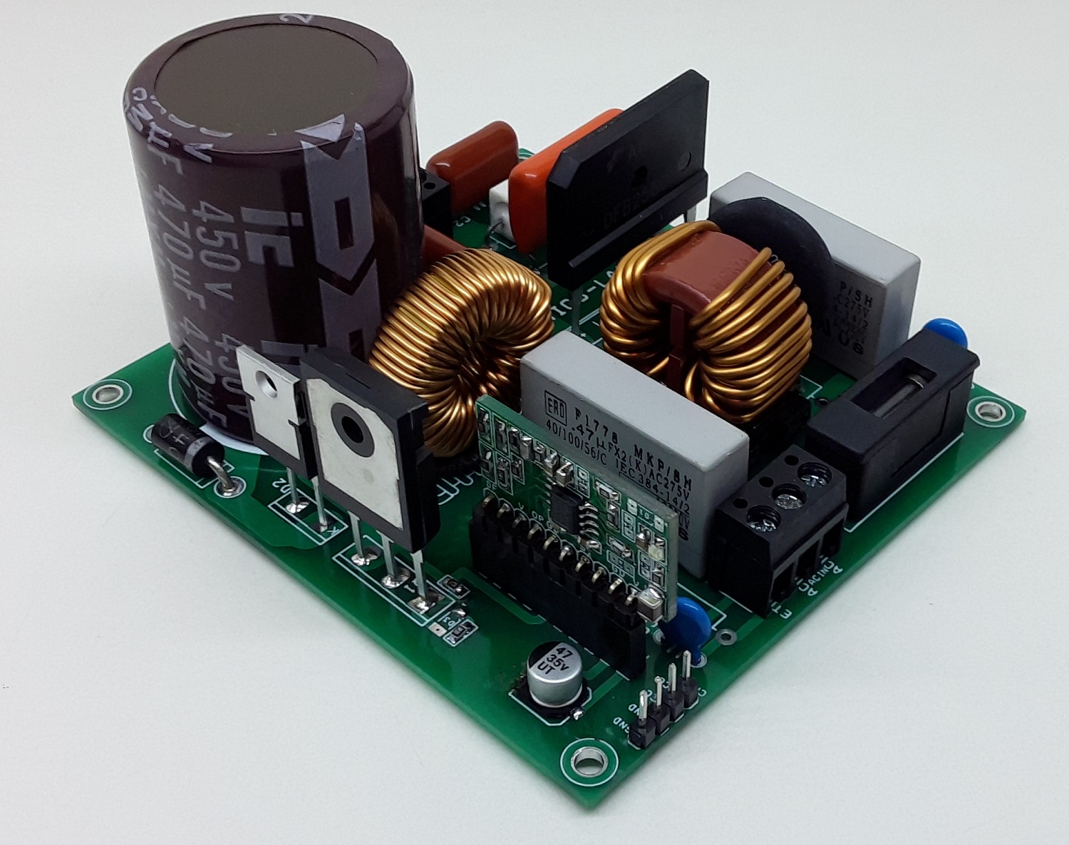
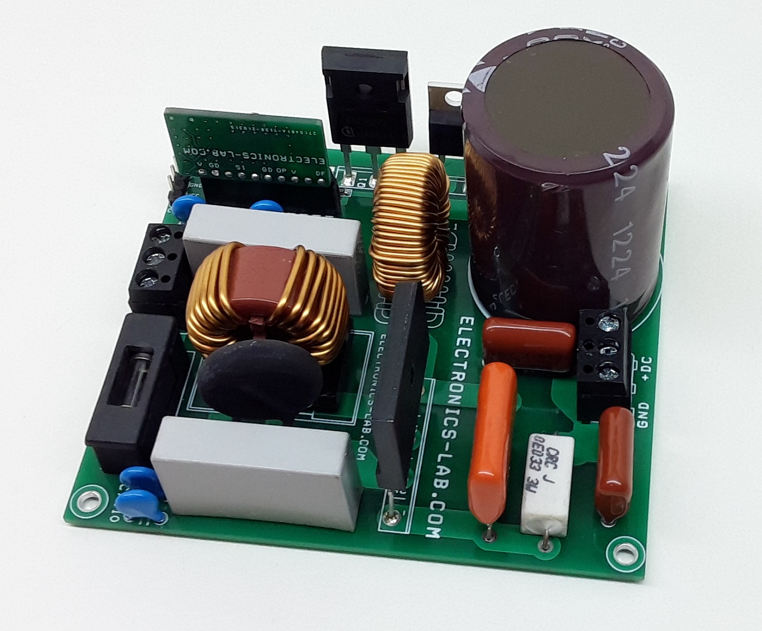
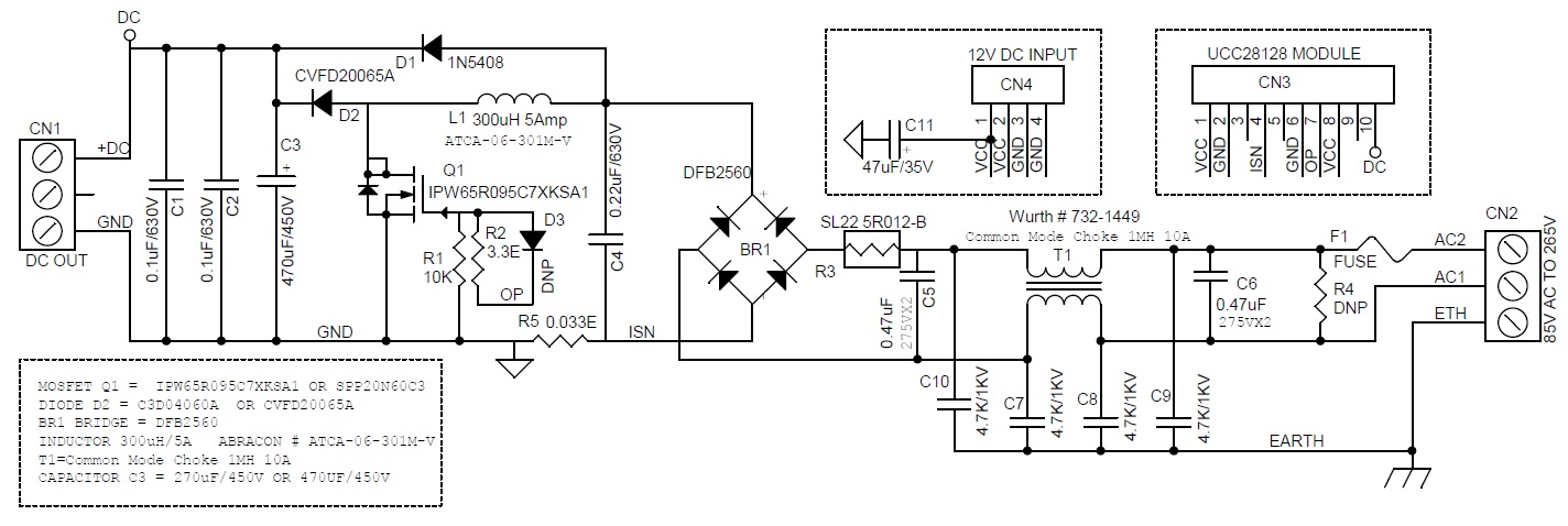
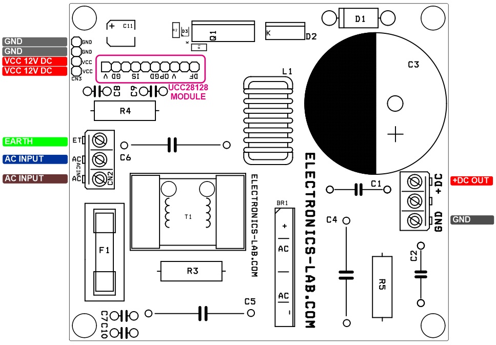
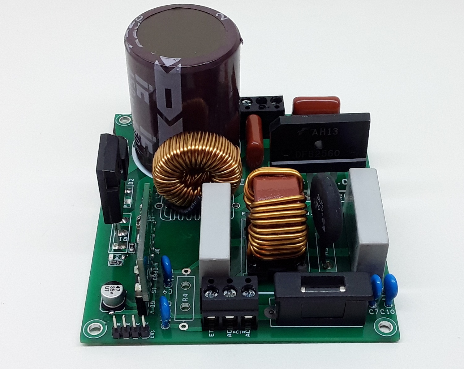
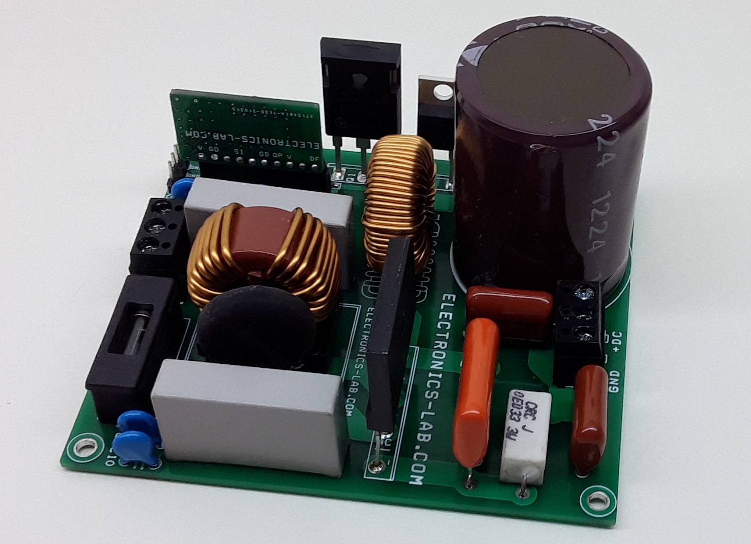
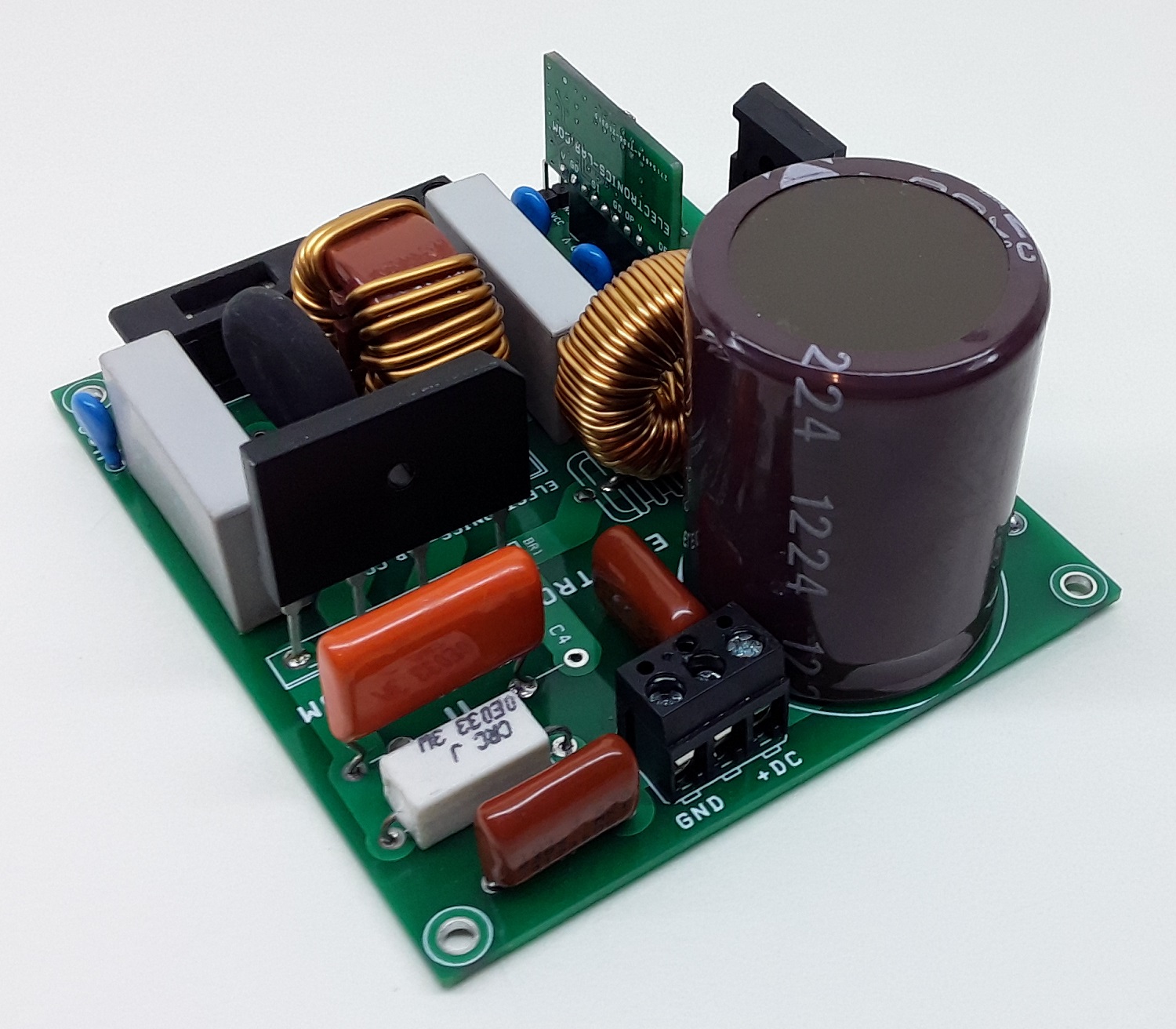
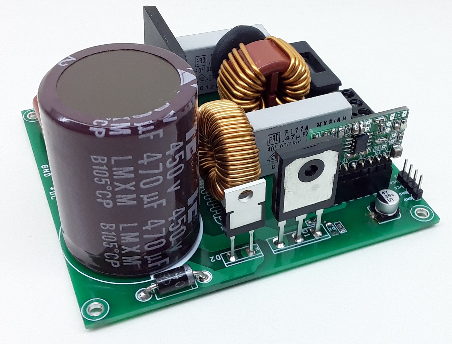
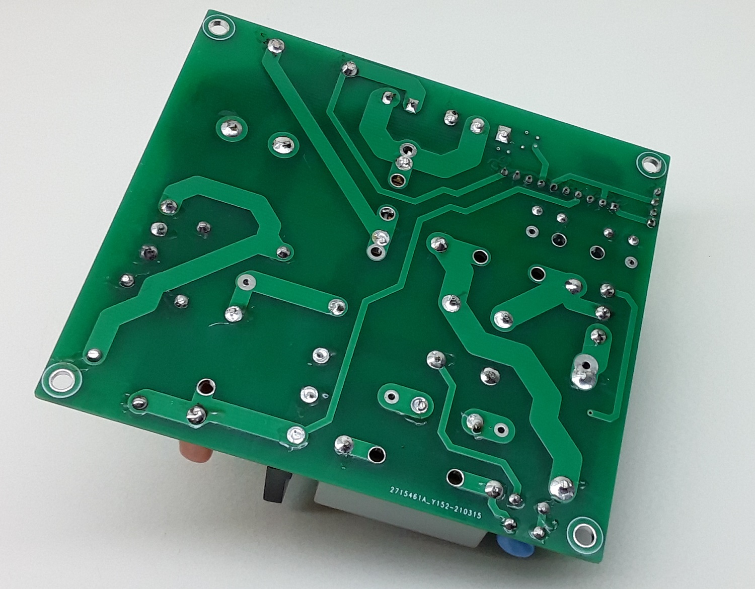
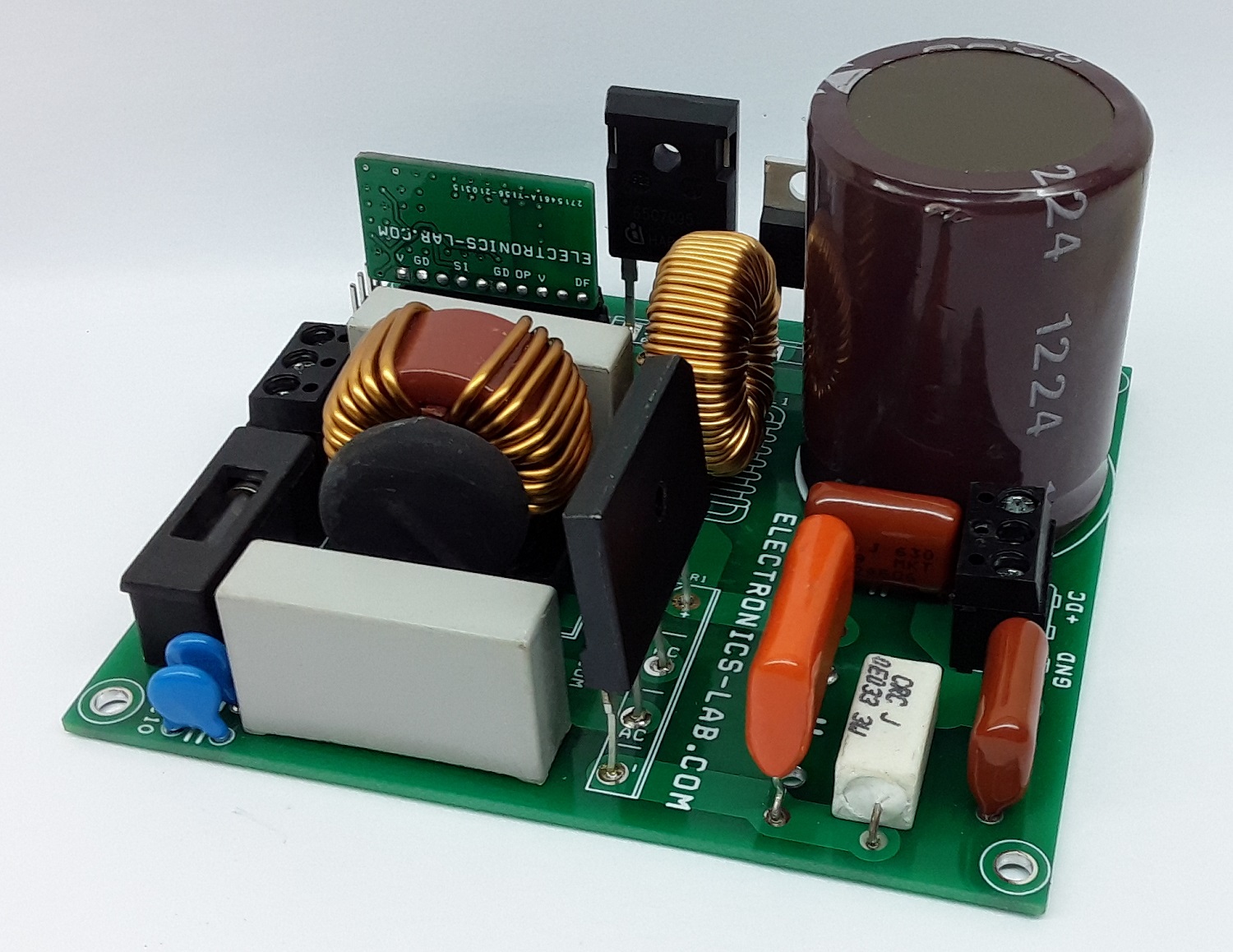
The circuit presented here is a 300W off-line power factor correction (PFC) boost converter providing a nominal regulated output voltage of 375V@ 0.8A of load current. The project accommodates an input voltage range of 85V AC to 265VAC and uses average current mode control at a fixed programmable switching frequency of 116KHz. The project is based on UCCC28180 PFC controller module which incorporates a wide range of protection features to ensure safe system operation. The controller operates under average current mode control at a fixed programmable switching frequency of 116 kHz. Simple external current and voltage loop compensation, along with advanced protection features, make this controller ideal for server and desktop power supplies, industrial power supplies, and white goods. The project includes onboard fuse for short circuit protection, EMI filter, NTC to control inrush current, Bridge rectifier for DC rectification, high voltage/current MOSFET for switching, switching diode, high current inductor, high-value DC bus filter capacitor on the output. This project requires UCC28128 based controller board that can be mounted vertically on the PCB socket.
300W Off-line Power Factor Correction (PFC) Boost Converter – [Link]
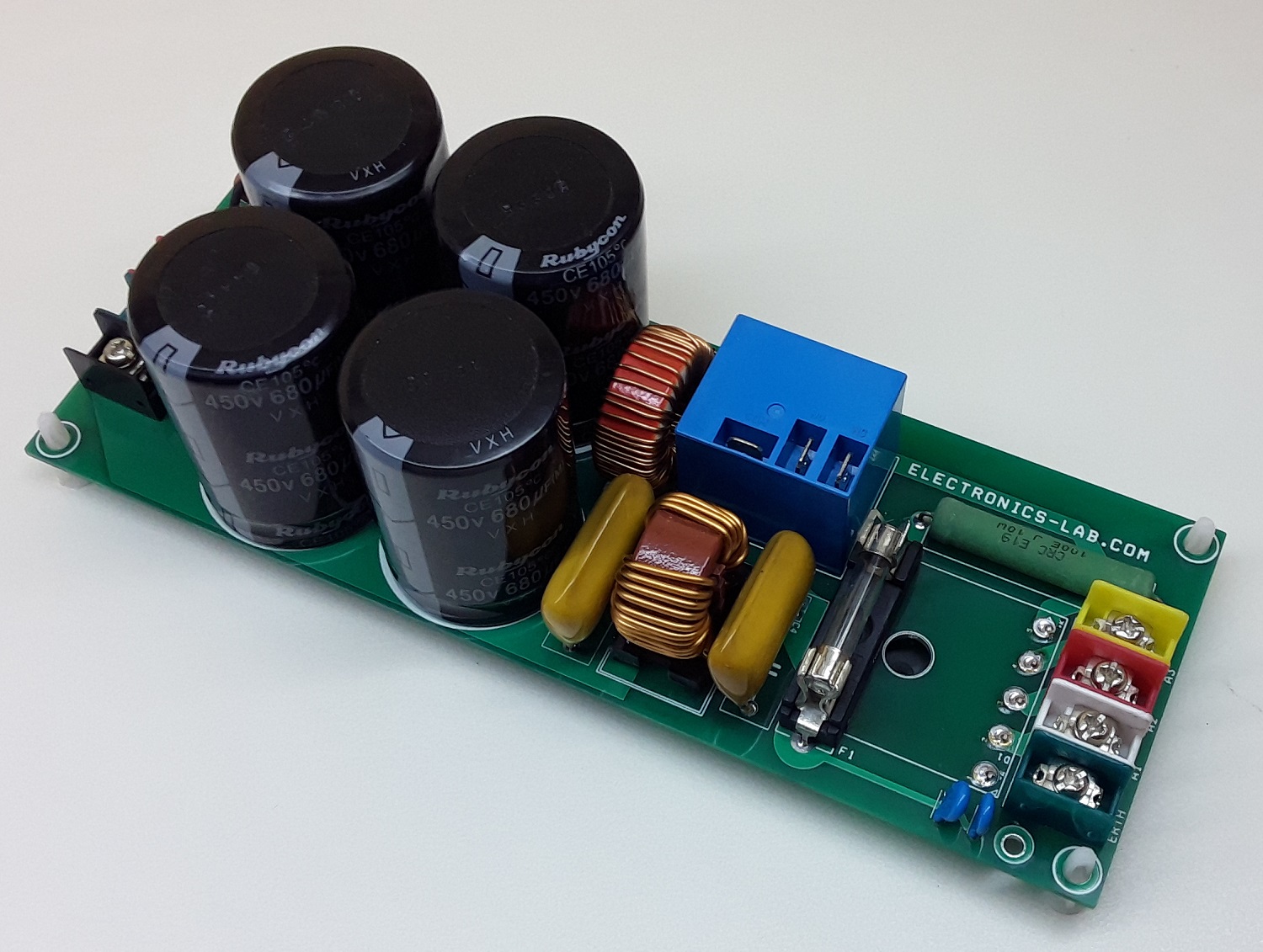
Although this power supply design is specific to the Intelligent Power Modules (IPM) VFD drives, high voltage boost converters, high voltage battery chargers, etc, the concept and circuit design may be used for any power supply that requires a high voltage output of up to 800V DC and 4 A. Since it is an unregulated power supply the output will depend on AC input voltage. The circuitry includes a passive EMI filter consisting of elements C8, C9, C4, T1, and L1. Bridge rectifier D1, R1 for inrush current protection, and a relay RL1 for soft powering up and reducing conduction losses in steady-state. 4 x electrolytic capacitors C2, C3, C6, C7 are used for buffering the rectified DC bus voltage, bleeding resistors R1, and R2 provided to discharge the DC bus capacitor after power off. It is advisable to use a heatsink for the bridge rectifier. Inrush current circuit requires 12-15V DC @ 80mA. Choose appropriate fuse as per current requirement. The relay takes care of the inrush current. It is important to switch ON the 12V-15V DC and 3phase power same time.
3 Phase AC input – DC Output – High Voltage DC Power Supply (2KW) – [Link]
This is an easy-to-build project and it is the most cost-effective and high-performance frequency multiplier, which instigates analog phase lock loop techniques. The circuit provides high-quality, high-frequency output from lower frequency crystal or clock input. The project can be used as a crystal frequency oscillator, clock multiplier and frequency translation. Using phase-locked-loop (PLL) techniques, the device uses a standard fundamental mode, inexpensive crystal to produce an output clock up to 200Mhz. On-board jumpers are provided to select from nine different multiplication factors, which output many common frequencies. The device also has an output enable pin that tri-states the clock output when the enable pin is taken low. The chip is intended for clock generation and frequency translation with low output jitter.
Clock Multiplier – Crystal Frequency Generator using PT7C4511 – [Link]
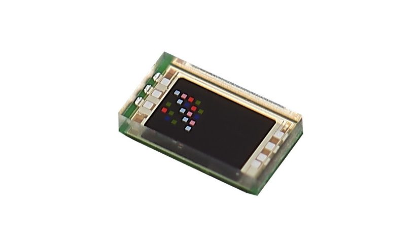
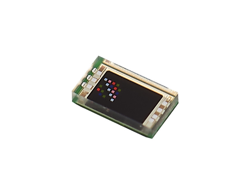
STMicroelectronics’ color sensor with advanced light flicker extraction is fast and accurate thanks to an individual ADC
STMicroelectronics’ VD6283 (1.83 mm x 1.0 mm x 0.55 mm) is a color sensor with advanced light flicker extraction. Light measurement is fast and accurate thanks to an individual ADC and a readout for each color channel. The VD6283 uses hybrid color filters with precise responses allowing accurate computation of the correlated color temperature (CCT) and Lux information. The VD6283 can be used for display brightness management or scene light correction.
With a patented architecture and a high-performance photodiode design, the VD6283 can extract light flickering frequencies to avoid banding effects on videos or check that they are safe for the human eye. Additionally, the VD6283 is the only sensor able to extract different light flicker waveforms from 100 Hz and 2 kHz, including LED square signals, that can run flicker operations simultaneously with ALS operations.
Features
Miniature optical module
1.83 mm x 1.0 mm x 0.55 mm
Optical BGA, 6-balls, reflowable package
Operates with cover glass on top
ALS operation with 6 independent channels (red, green, blue, IR, clear, and visible)
Advanced hybrid filters with high photocount response
Operating conditions: 7 mLux to 30 kLux (green channel)
Light flicker extraction
Innovative readout architecture to extract AC light flicker signal
From 100 Hz to 2 kHz frequency detection, sine or square wave
Software driver provided by ST
I²C interface up to 1 Mbit/s (Fast mode plus)
1.8 V power supply
Operating temperature: -30°C to +85°C
Applications
Screen brightness control for personal electronics
Auto white balance color for displays or cameras
Light flicker removal for cameras
Scene light correction thanks to Lux and CCT measurement
IoT display brightness control for power saving
Light control for smart buildings or greenhouses
Predictive maintenance for light aging
Light flicker frequency extraction to check eye-safety
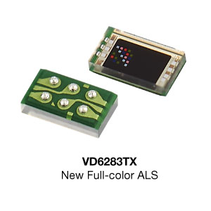
Cost-effective dimmable and intelligent LED systems are expected to increase the market share disproportionately in the coming years. Introducing the ICL8800, ICL8810 and ICL8820 single-stage flyback LED controllers for constant output voltages, Infineon Technologies AG addresses the need of LED driver manufacturers in this regard. With their unique features, the ICs meet the necessary performance requirements for LED lighting applications, such as LED drivers and luminaires up to 125 W, smart lighting, and emergency luminaire. Outside this market segment, adapters and chargers, flat TVs, all-in-one PCs and monitors up to 125 W profit from the ICL88xx family.
All three variants offer benchmarking performance for power factor correction and total harmonic distortion at full-load and low-load conditions, thus enabling platform design and window drivers. They are optimized as secondary-side regulated (SSR) constant voltage (CV) output flyback controllers and are also well suited for primary-side regulation (PSR). To achieve optimum efficiency and low electromagnetic interference (EMI) without compromising light quality, they are featuring critical conduction mode (CCM) and quasi-resonant mode (QRM) with smart valley hopping.
The ICL88xx family offers an external start-up circuit control signal for more flexibility and a cost-optimized bottom-up platform design for many applications. It has a comprehensive set of protection features, including a power limitation and secondary side over-voltage protection. In addition, the devices require a minimum number of external components, leading to outstanding cost-effectiveness compared to existing solutions. The gate driver current enables designs up to 125 W with state-of-the-art MOSFETs. The system performance and efficiency can be further optimized using Infineon’s CoolMOS™ P7 power MOSFETs.
ICL8800 is the basic variant providing all of the above features. ICL8810 is an advanced variant with an integrated burst mode that allows a very low standby power consumption of less than 100 mW and flicker-free deep dimming down to 0.1 percent. This feature makes ICL8810 ideally suited for smart lighting applications in connection with microcontrollers. Finally, ICL8820 is the fully-featured variant, additionally equipped with an integrated DC-input jitter function. The latter improves EMI performance and supports the fulfillment of EMI requirements in DC operation. ICL8820 eases EMI certification in the design of emergency lighting LED driver applications without additional circuitry, minimizing cost and effort.
Availability
ICL8800, ICL8810 and ICL8820 single-stage flyback LED controller variants are available in PG-DSO-8 packages and can be ordered now. More information is available at www.infineon.com/icl88.
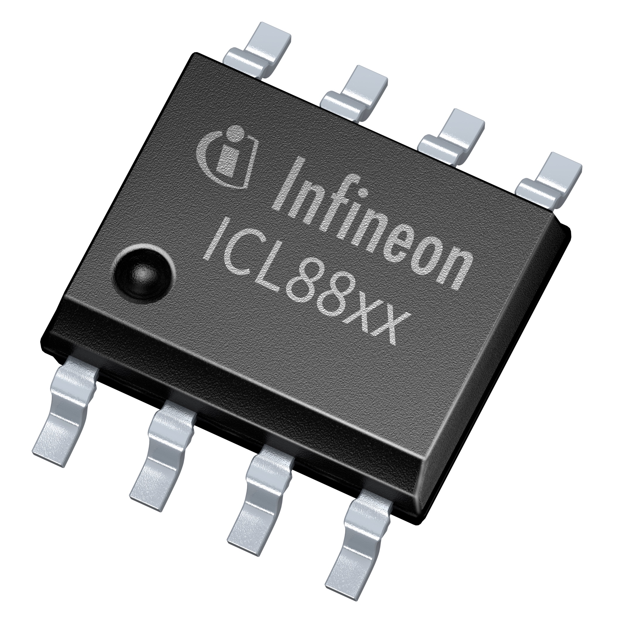
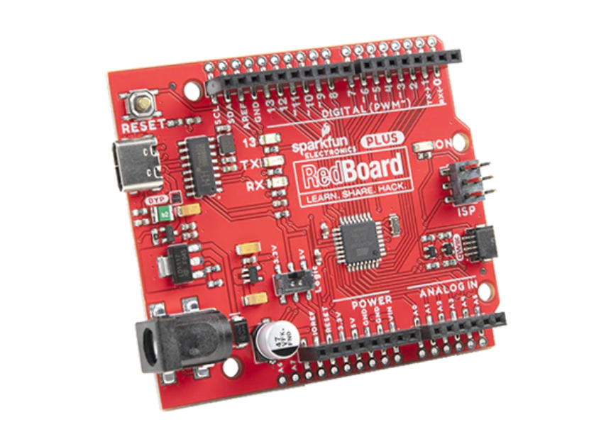
SparkFun RedBoard Plus Development Board is an Arduino-compatible board that is similar to an Arduino Uno with many extra perks. This DEV-1858 development board utilizes a handy Qwiic Connect System that means no soldering or shields are required to connect it to the rest of the system. The RedBoard Plus board includes the hardware peripherals like 22x digital I/O pins with 6x PWM pins, 8x analog pins, UART, I2C, SPI, and external interrupts. This board uses the LM1117 5V voltage regulator and AP2112 3.3V voltage regulator that provides up to 600mA to daisy chain multiple Qwiic boards and sensors. The RedBoard Plus board comes with an I/O voltage switch also known as the “Red Squirrel” switch. This Red Squirrel switch can easily select the GPIO voltage between 3.3V to 5V.
The RedBoard Plus can be programmed over a USB-C cable with 5V input voltage or through the barrel jack from 7V to 15V input voltage. This development board features 32kB flash memory, 16MHz clock speed, all SMD construction, R3 shield compatibility, and an improved reset button.
Features
ATmega328P MCU with Optiboot (UNO) bootloader
Input voltage:
7V to 15V via barrel jack
5V via USB-C
Voltage regulators:
LM1117 adjusted to 5V
AP2112 for 3.3V
Built-in resettable PTC fuse 5V/2A
CH340G Serial-to-USB converter
3.3V to 5V logic level switch
22x digital I/O pins:
6x PWM outputs, 8x analog inputs, UART, I2C, and SPI
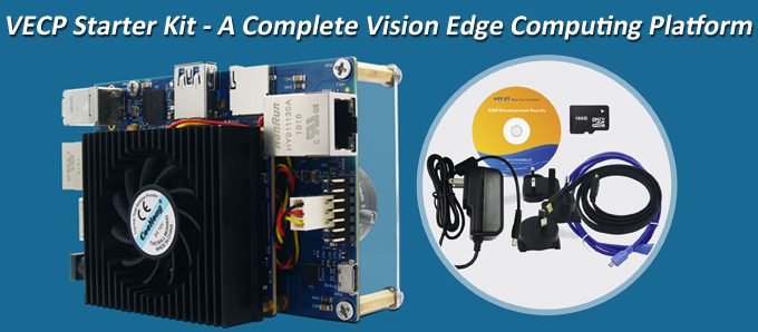
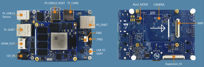
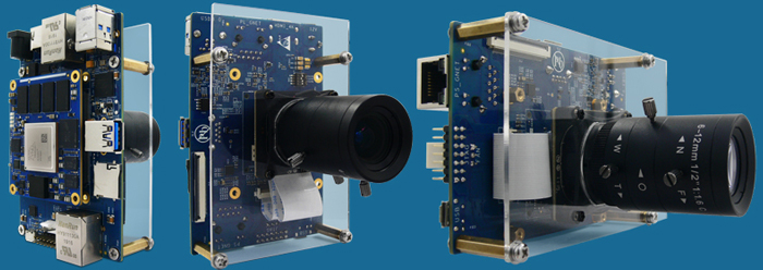
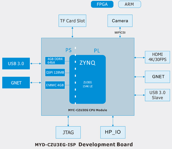
MYIR introduces the VECP Starter Kit, a complete Vision Edge Computing Platform designed to support excellent image processing for typical applications like Machine Vision, Industry, IoT, Medical and more others in different areas of business and everyday life.
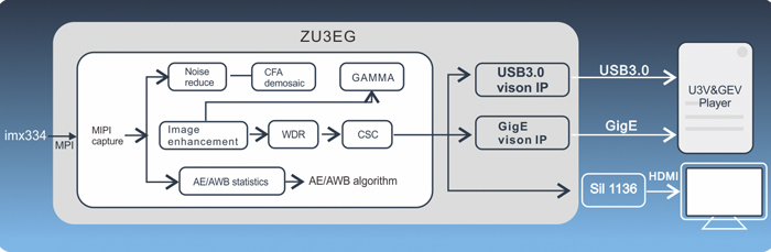
The VECP Starter Kit is using Xilinx Zynq UltraScale+ ZU3EG solution and comes with a MYD-CZU3EG-ISP development board as well as some accessories to help users start their development rapidly. The MYD-CZU3EG-ISP board consists of a MYC-CZU3EG CPU Module with installed active heatsink, a base board and a SONY imx334 4K Sensor which is installed on the rear of the base board and connected to the board MIPI-CSI interface through an FPC cable. The board is ready to run Linux OS and provided with plenty of software resources.
The MYD-CZU3EG-ISP development board shows outstanding image processing performance through the built-in ISP core which is capable of handling 4K video at 30fps and implementing ultra-low delay video transmission at maximum 0.7ms. It also has integrated IP cores for high-speed video standards like GigE Vision and USB3 vision to allow the image transmission via the Gigabit Ethernet or USB 3.0 from the board FPGA logic part.
The VECP Starter Kit is offered at $599/unit only. MYIR also offers custom design services for board design based on the MYD-CZU3EG-ISP development board or customized image sensors or customized IP cores according to customers’ requirements.
For whatever deep learning purpose or production, the VECP Starter Kit will be easy for users to begin their edging computing experience and reduce their time to market with the design reference or system integration.
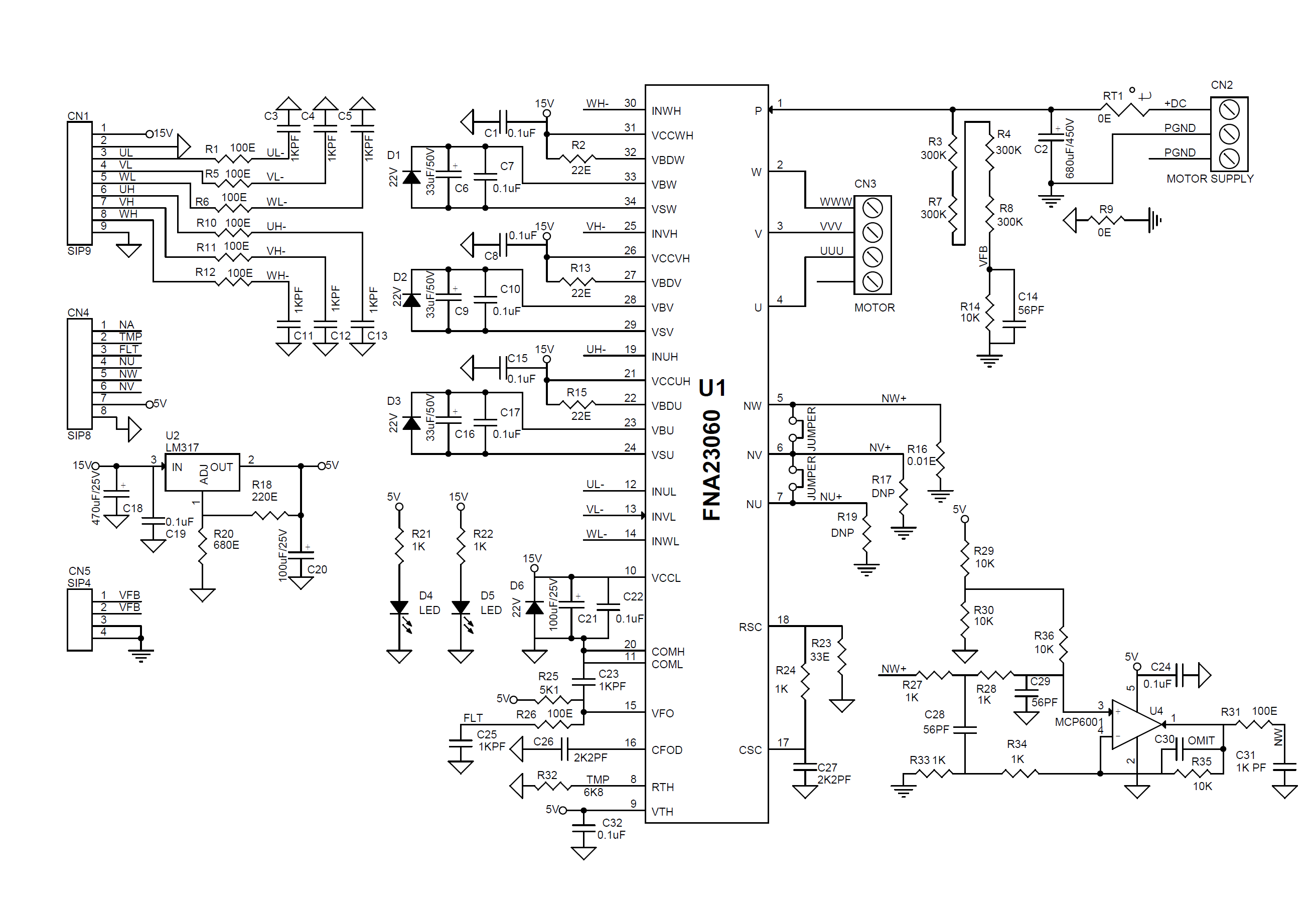
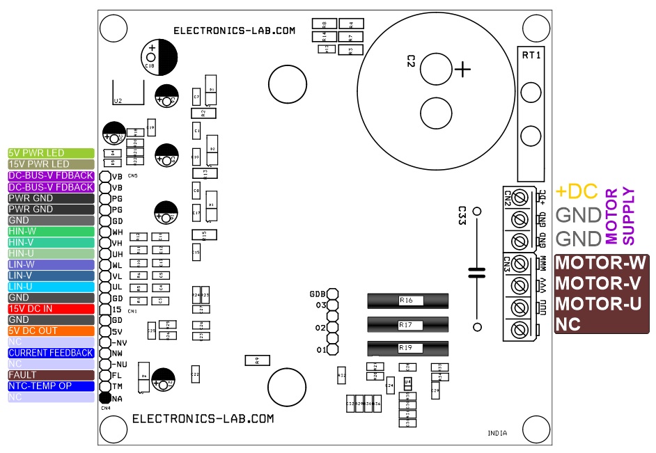
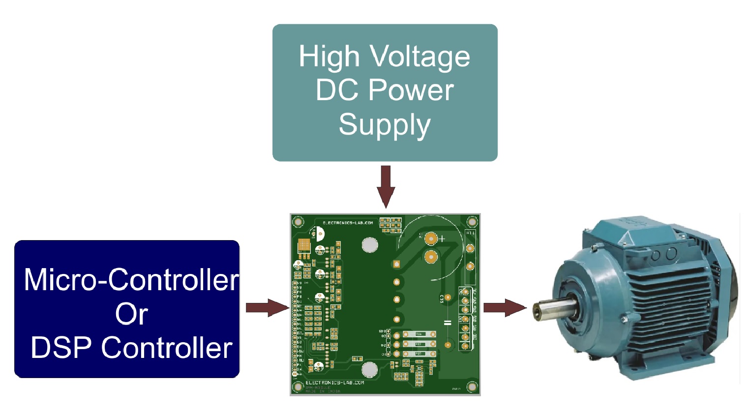
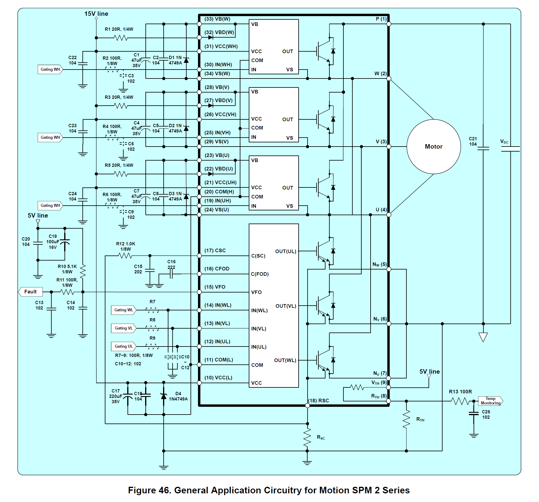
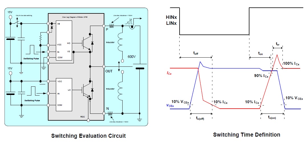
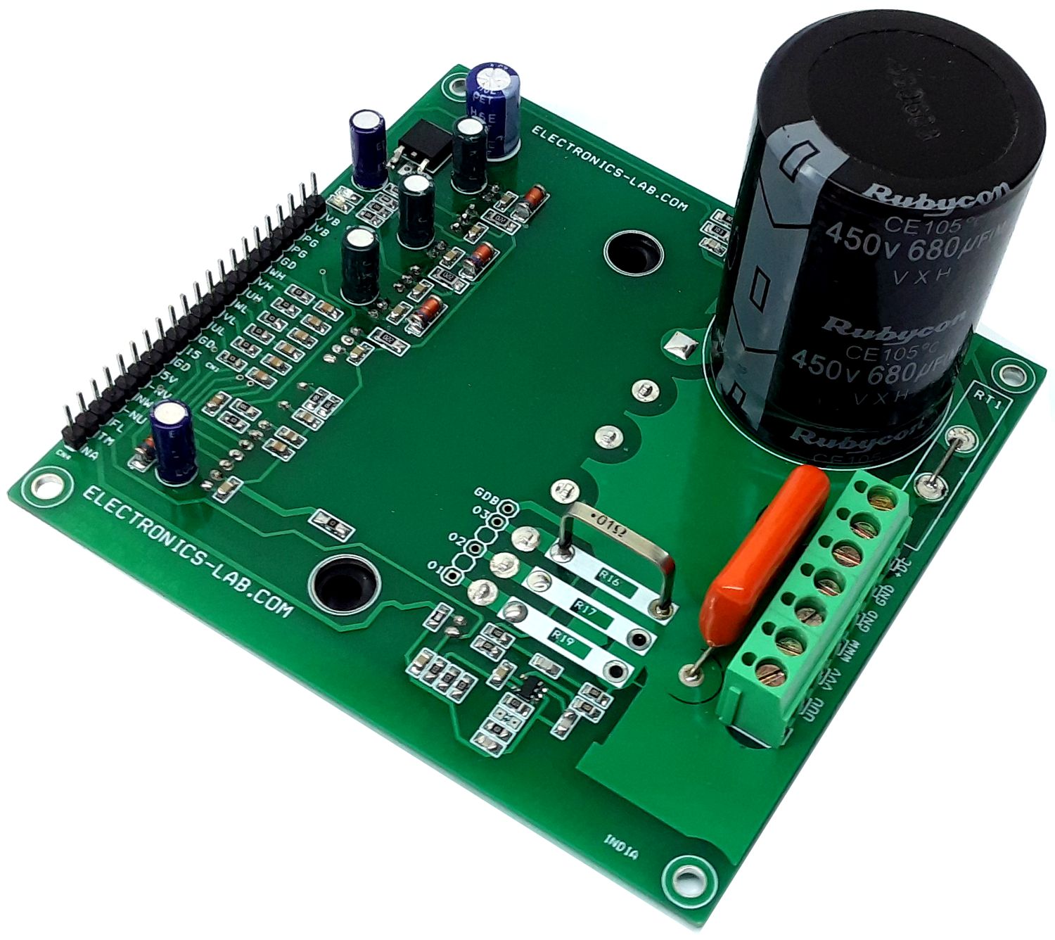
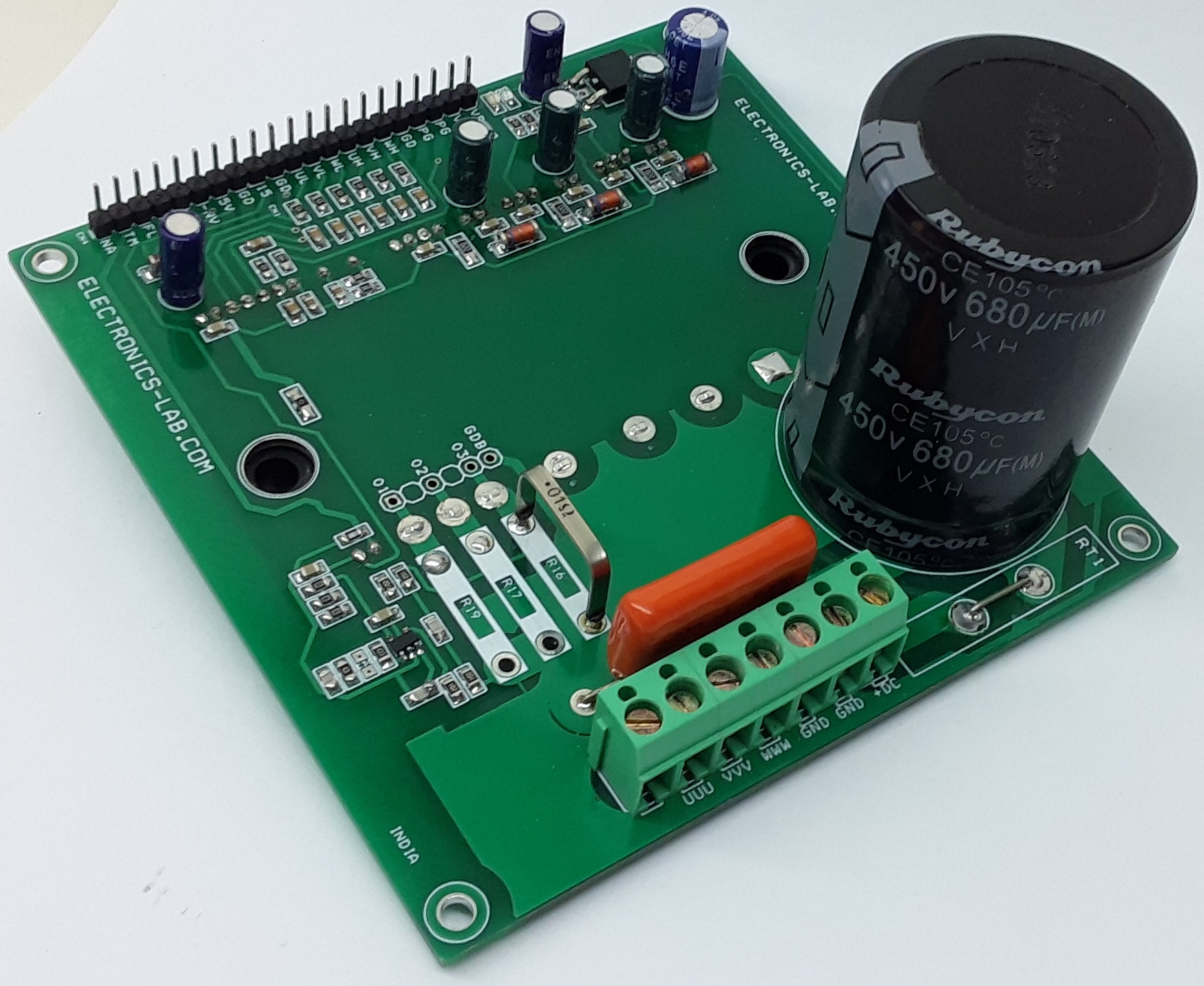
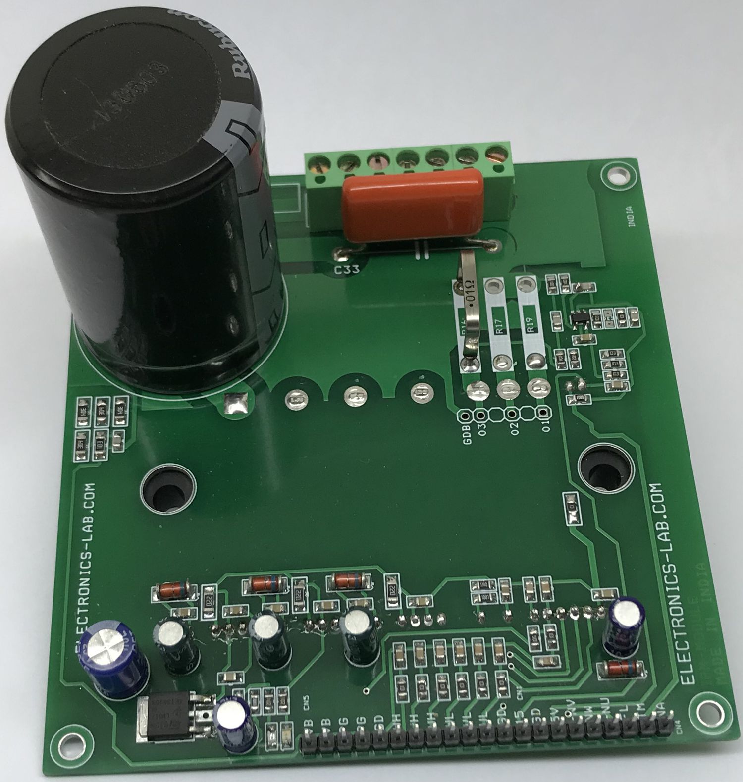
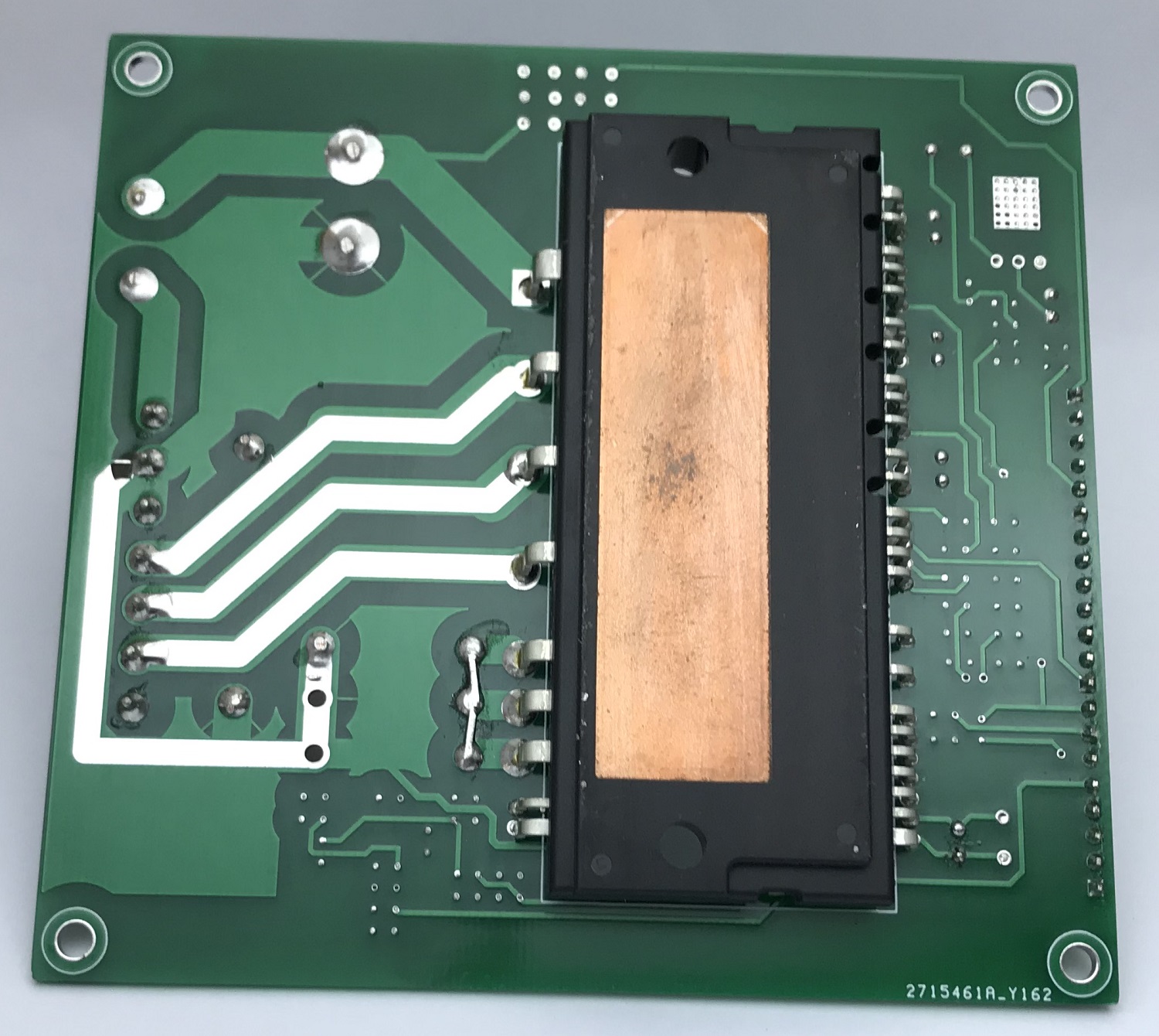
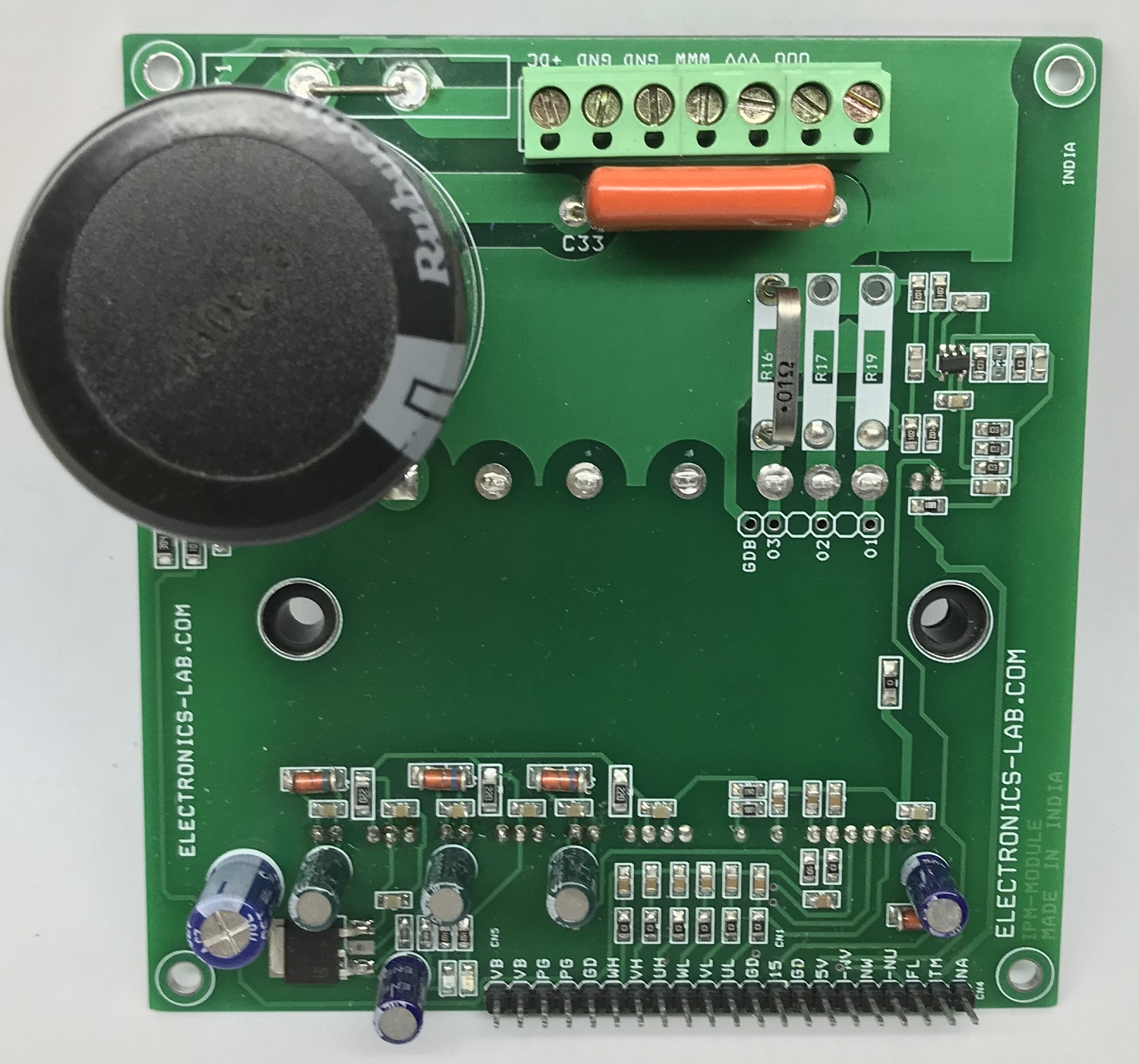
This compact IPM module circuit provides a fully-featured, high-performance inverter output stage for AC Induction, BLDC, and PMSM motors. The circuit is based on FNA23060 chip which integrates the optimized gate drive of the built-in IGBTs to minimize EMI and losses, while also providing multiple on-module protection features: under-voltage lockouts, over-current shutdown, temperature sensing, and fault reporting. The built-in, high-speed HVIC requires only a single supply of 15V and translates the incoming logic-level gate inputs to high-voltage, high-current drive signals to properly drive the module’s internal IGBTs. On-Board optional current sense circuit can be used to monitor the current. LM317 regulator provides 5V DC output to drive op-amp current sense circuit. LED D4 and D5 indicate 5V power and 15V power. Board has an option for 3 current sense resistors. An external 3 phase current circuit is required for 3 phase current sense circuit, if a single current sense circuit is required, solder all 3 phase NU+, NV+, NW+ together and use U4 op-amp circuit, in this case, solder R16. The current sense circuit is built using op-amp based, the gain of the circuit can be set as per user requirement. The board works with lethal high voltage DC and requires extra care while testing. PFC-based DC power supply is recommended to power the board.
Note: It is advisable to read the datasheet of FNA23060 to configure and control this board, current trip, Fault output, input PWM sequence, Over temperature output.
The board operates at lethal voltages and has bulk capacitors that store significant charge. Accidental contact can lead to lab equipment damage, personnel injury, and may be fatal. Please be exceptionally careful when probing and handling this board. Always observe normal laboratory precautions.
Features
Operating Supply Motor 90V to 390V DC
IPM Load Current Maximum 30Amps (Approx. 2.2KW Motor Rating)
Logic Supply 15V DC
Motor Supply (Bus-Voltage Feed-Back Output 3.2V when Bus 390V, 0.75 when Bus V=90V)
On-Board Current Sense Circuit
Current Sense Output 1.7V at 0 Amp 100mV/Amp Approx.
2X Power LEDs for 15V and 5V
Fault Output Normally High Goes Low When Fault Condition Occurs
Inbuilt Thermistor for over Temperature 47K Ohms @ 25 Degree Centigrade, 2.9K @ 100 Degree Centigrade
Over Temperature Protection Output
Operating Frequency up to 20Khz
PCB Dimensions 100.17 x 104.93 mm
Current Sense: the board has provision to mount 3 shunt resistors if 3 phase current monitor is required, in this case, use R16, R17, R19 resistors. This will require 3 phase current to voltage op-amp circuit, the board has provision to measure a single current sense, in this case, solder all 3 emitters of IGBTs (Pin 5,6,7) and use U4 op-amp circuit to monitor the current of the motor.
Over Current: The IPM module has an inbuilt separate over-current shutdown circuit, over-current is set using R23, R24, and C27, refer to datasheet of IC to calculate the Over Current shutdown threshold as per requirement.
Signal Input Pins: Pins IN(UL), IN(VL), IN(WL), IN(UH), IN(VH), IN(WH), These pins control the operation of the built−in IGBTs. They are activated by voltage input signals. The terminals are internally connected to a Schmitt−trigger circuit composed of 5 V−class CMOS. The signal logic of these pins is active HIGH. The IGBT associated with each of these pins is turned ON when a sufficient logic voltage is applied to these pins. The wiring of each input should be as short as possible to protect the Motion against noise influences. To prevent signal oscillations, RC (Resistors and capacitors) R1, R5, R6, R11, R12, R13, C3, C4, C5, C11, C12, C13) provided at all 6 inputs signals.
Power Supply: 15V DC supply required to drive the Logic gate driver circuit Use Pin 1and 2 of connector CN1 to apply logic supply. U2 LM317 regulator provides 5V DC to op-amp circuit for current sense. CN2 screw terminals are provided to power the load.
Power LED: D4 5V LED, D5 15V LED
Motor Supply Voltage Feedback: CN5 Connector provides Bus voltage (Motor Supply) feedback (Output 3.2V when 390V, 0.75V when Bus V=90V)
Motor Connections: 4 Pin screw terminal CN3 for motor connections, pin 1 motor phase W, pin 2 motor phase V, pin 3 motor phase U
Heatsink: Large size heatsink and fan is very important to cool down the IPM module.
Arduino Connections and Code
We tested the board with Arduino UNO board and ARDUINO_UNO_Code.zip. Please follow the instructions below to connect Arduino with the IPM board.
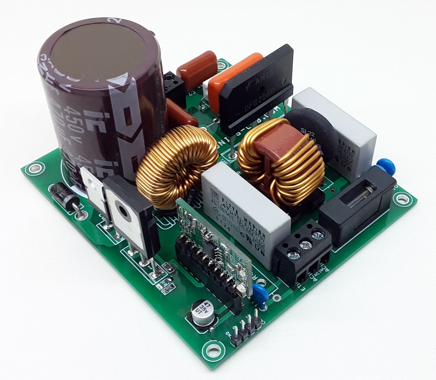
The circuit presented here is a 300W off-line power factor correction (PFC) boost converter providing a nominal regulated output voltage of 375V@ 0.8A of load current. The project accommodates an input voltage range of 85V AC to 265VAC and uses average current mode control at a fixed programmable switching frequency of 116KHz. The project is based on UCCC28180 PFC controller module which incorporates a wide range of protection features to ensure safe system operation. The controller operates under average current mode control at a fixed programmable switching frequency of 116 kHz. Simple external current and voltage loop compensation, along with advanced protection features, make this controller ideal for server and desktop power supplies, industrial power supplies, and white goods. The project includes onboard fuse for short circuit protection, EMI filter, NTC to control inrush current, Bridge rectifier for DC rectification, high voltage/current MOSFET for switching, switching diode, high current inductor, high-value DC bus filter capacitor on the output. This project requires UCC28128 based controller board that can be mounted vertically on the PCB socket.
Heat Sink: Use appropriate heatsink for MOSFET and Switching Diode.
Fan: A fan, capable of 200 LFM to 400 LFM, should be used to maintain component temperatures within safe operating ranges at all times during operation.
Note: This project has 2 blocks, the power board and controller board, information about controller board is available here
The board operates at lethal voltages and has bulk capacitors that store significant charges. Accidental contact can lead to lab equipment damage, personnel injury, and may be fatal. Please be exceptionally careful when probing and handling this board. Always observe normal laboratory precautions.
Features
AC Input Range 85V AC to 265V AC
AC Frequency 47Hz to 63Hz
DC Supply for Logic Circuit 12V DC @ 100mA
300W, 275V DC Output
Average Current Mode PWM Control
Fixed 116Khz Oscillator Frequency
Soft Over Current and Cycle-by-Cycle Peak Current Limiting
VCC Under-Voltage Lockout with Low Start-Up Current
Voltage Regulation Open Loop Detection
Output Over-Voltage Protection with Hysteresis Recovery
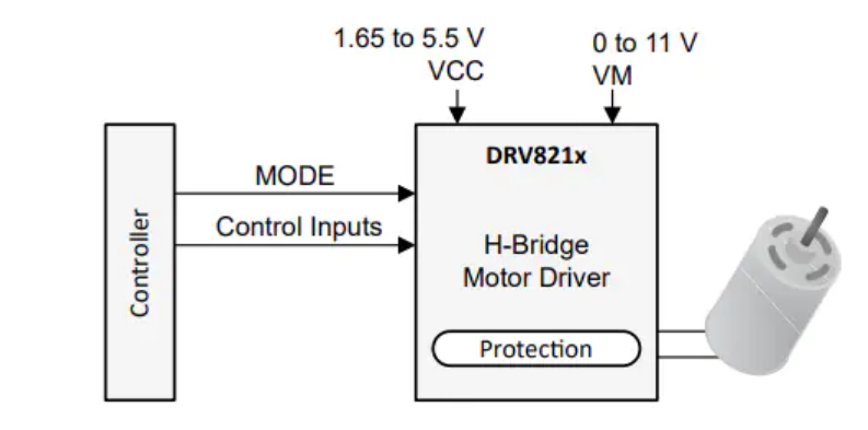
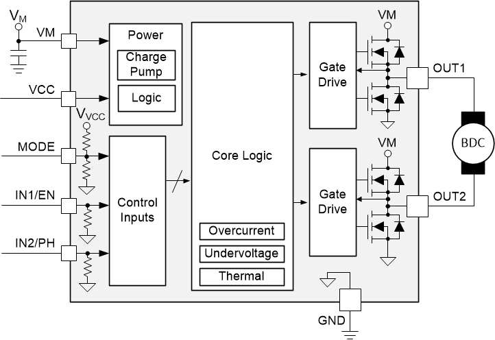
Texas Instruments DRV8212 12V, 2A Low Voltage H-Bridge Motor Driver provides PWM, PH/EN, and half-bridge control interfaces and low-power sleep mode. The DRV8212 Motor Driver is integrated with four N-channel power FETs, a charge pump regulator, and protection circuitry. The triple charge pump architecture allows the device to operate down to 1.65V to accommodate 1.8V supply rails and low-battery conditions. The charge pump integrates all capacitors to reduce the overall solution size of the motor driver on a PCB and allows for 100% duty cycle operation.
The TI DRV8212 supports multiple control interface modes including, PWM (IN1/IN2), phase/enable (PH/EN), independent half-bridge, and parallel half-bridge. Each interface supports a low-power sleep mode to achieve ultra-low quiescent current draw by shutting down most internal circuitry. The device supplies up to 4A peak output current and operates with a supply voltage from 1.65V to 5.5V.
Robust internal protection features are available on the DRV8212, including supply under-voltage lockout (UVLO), output overcurrent (OCP), and device overtemperature (TSD).
The DRV8212 is part of a family of devices that come in pin-to-pin scalable RDS(on) and supply voltage options to support various loads and supply rails with minimal design changes. This family of devices includes DRV8210, DRV8210P, DRV8212, DRV8212P, and DRV8220.
Features
N-channel H-bridge motor driver
MOSFET on-resistance: HS + LS 280mΩ
Drives one bidirectional brushed DC motor
Two unidirectional brushed DC motors
One single- or dual-coil latching relay
Push-pull and bistable solenoids
Other resistive, inductive, or LED loads
1.65V to 11V operating supply voltage range
High output current capability:
Full-bridge: 4A peak
Half-bridge: 4A peak per output
Parallel half-bridge: 8A peak
Multiple interfaces for flexibility and reduced GPIO