Maxim Integrated MAX77301 Lithium-ion Linear Battery Charger

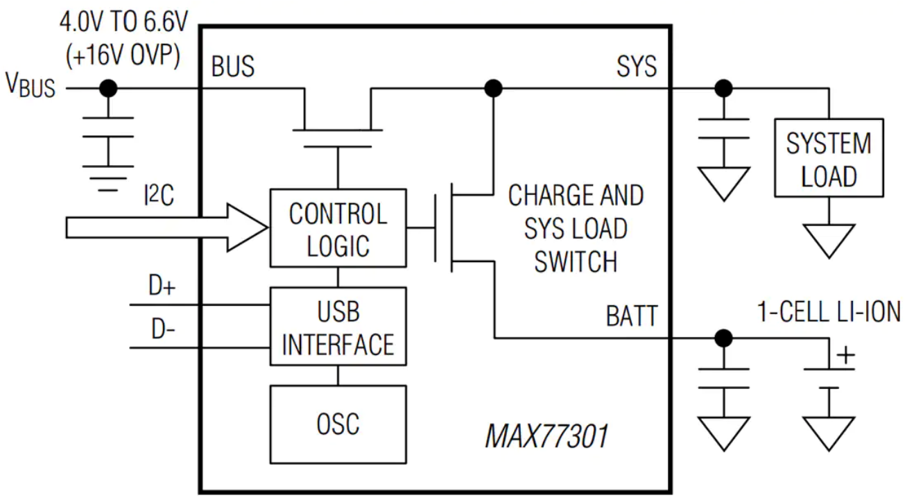
Maxim MAX77301 Lithium-ion Linear Battery Charger is JEITA-compliant and operates from a USB port, a dedicated charger, or a universal adapter. The IC provides automatic adapter-type detection and enumeration with a USB host or hub. The IC integrates an independent battery charge switch, current sense circuit, MOSFET pass elements, thermal regulation circuitry and eliminates the external reverse-blocking Schottky diode. This feature creates the simplest and smallest USB-compliant charging solution.

The Maxim MAX77301 includes automated detection of charge adapter type, making it possible to distinguish USB 2.0 devices, USB chargers, dedicated charger devices, as well as standard input adapters. When enumeration is enabled, the IC automatically negotiates with a USB host, making it possible to achieve the highest charging current available from a USB 2.0 device or USB charger without processor intervention. The adapter type detection is compliant with USB 2.0 as well as battery charging Specification Revision 1.1.
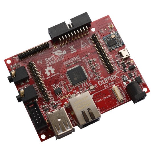
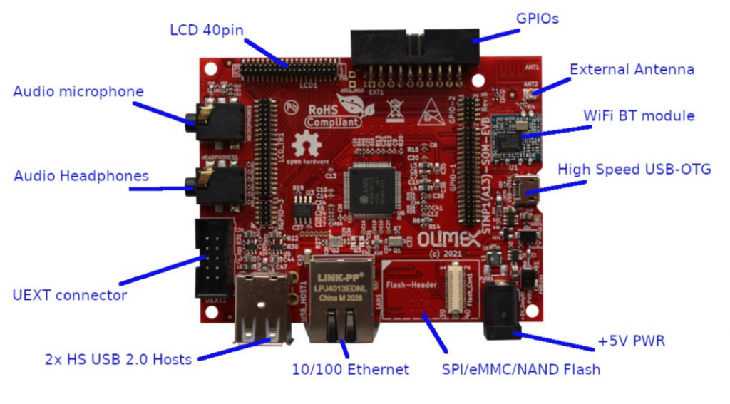
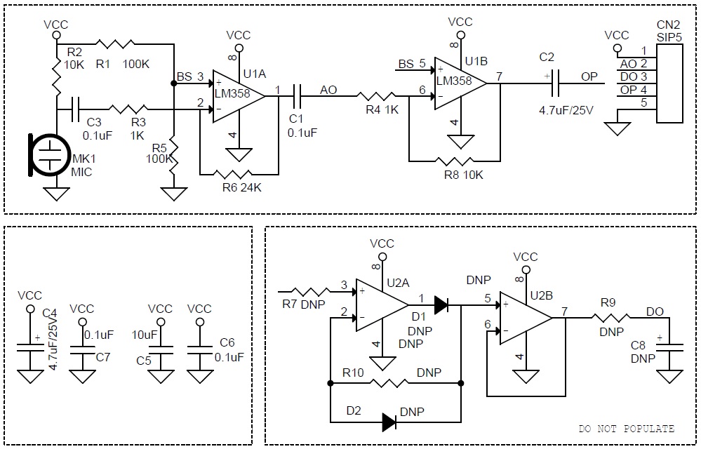
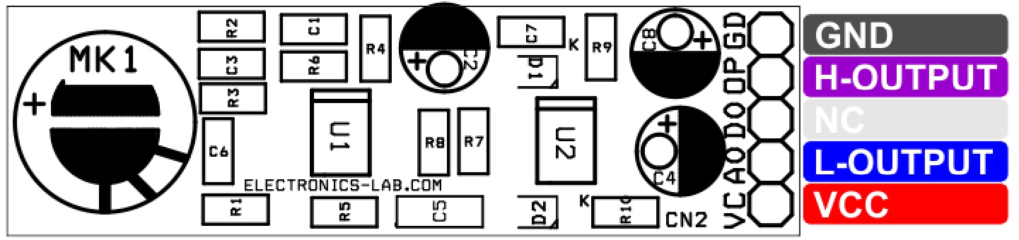
Block Diagram

The IC controls the charging sequence for single-cell Li+ batteries from battery detection, pre-qualification, fast charge, top-off, and charge termination. Charging is controlled using constant current, constant voltage, and constant die-temperature (CCCVCTj) regulation for safe operation under all conditions. The IC is also compliant with JEITA battery charging requirements.

Features

  • Enables charging from a USB port
  • Automatic detection of adapter type
  • Input current up to 1500mA and charging current up to 900mA
  • Enumeration without processor intervention
  • Supports USB low-speed and full-speed
  • Compliant with USB 2.0 specification and battery charging specification (Revision 1.1)
  • Compliant with next-generation low-voltage Li-Ion battery profiles
  • Input overvoltage protection up to 16V
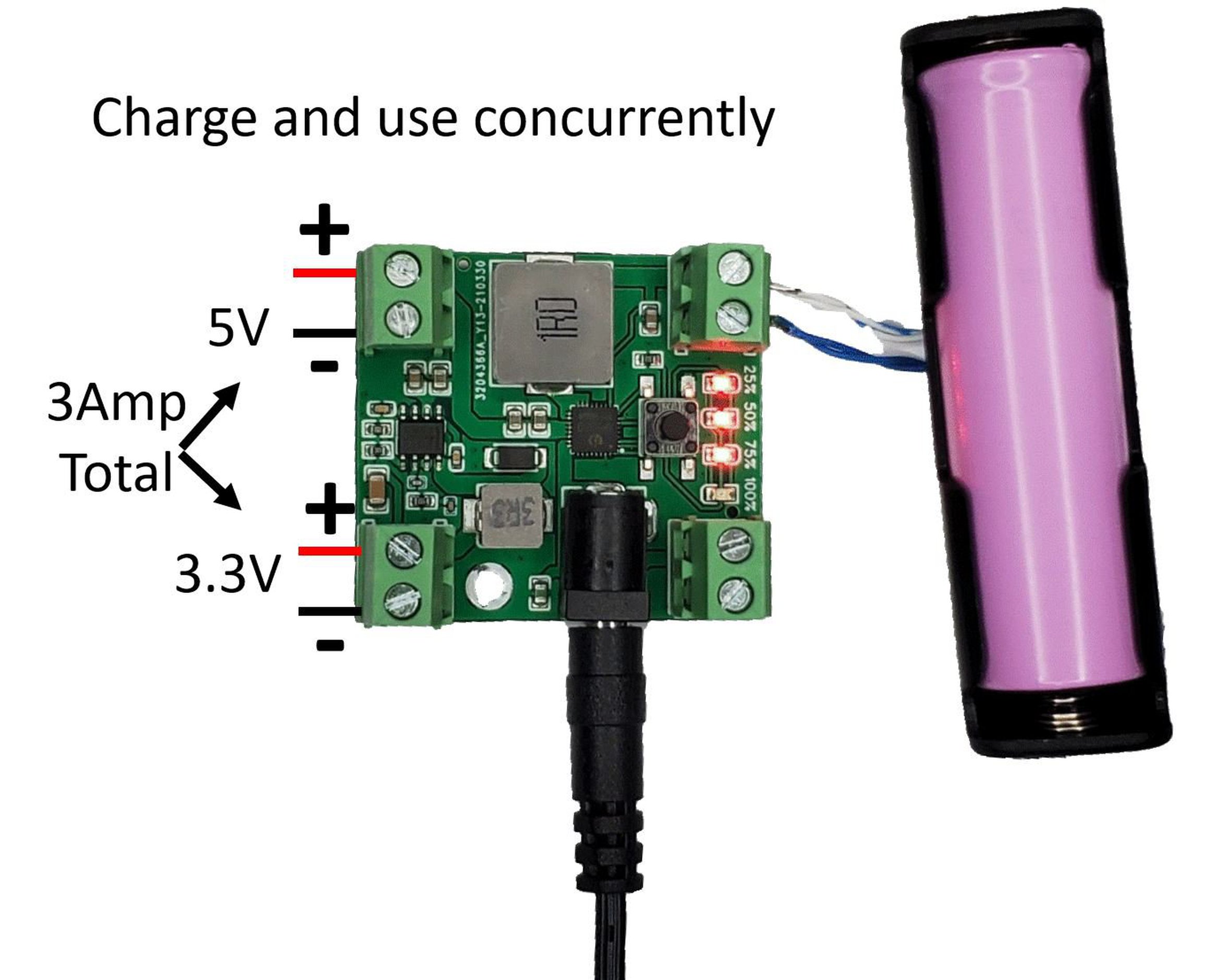
  • Smart Power Selector™ allows power path operation with discharged or no battery
  • Battery detection including packs with open protectors
  • Thermal regulation prevents overheating
  • LED indicator for charge done, precharge, and time/temperature error
  • Serial (400kHz) I2C-compatible interface
  • 6µA (Typ.) shutdown current
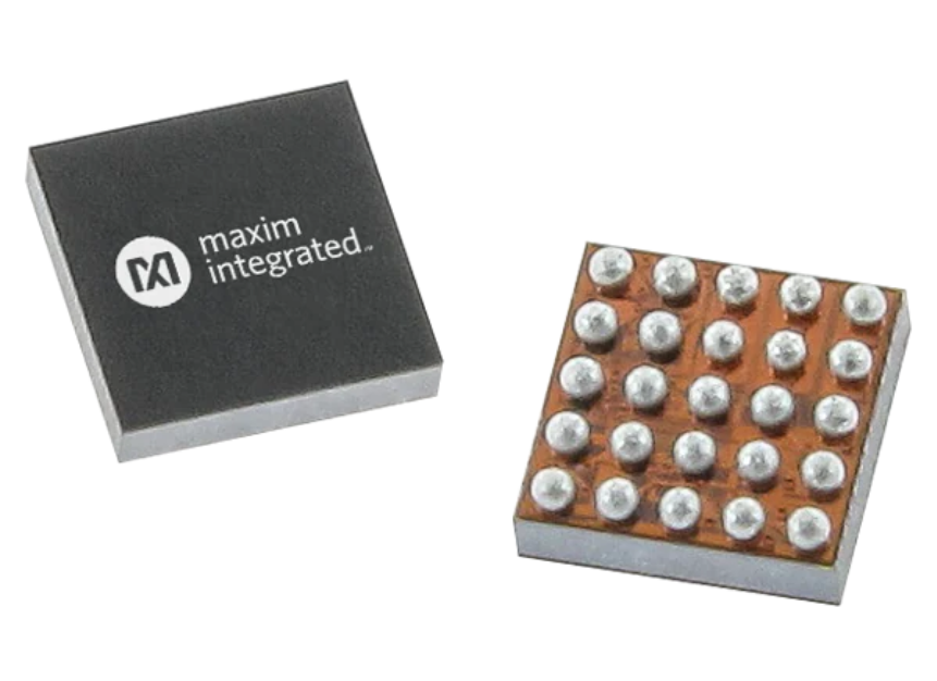
  • 2.44mm x 2.44mm, 25-Bump WLP package

The Smart Power Selector feature makes the best use of limited USB or adapter power. The battery charge current is set independent of the input current limit. Power not used by the system charges the battery. The battery assists the input source when needed. System voltage is maintained by allowing the application to operate without a battery, a discharged battery, or a dead battery. Automatic input selection switches the system from battery to external power.

The I2C interface provides full programmability of battery charge characteristics, input current limit, and protection features. This feature provides flexibility for use with a wide range of adapter and battery sizes.
Other features include undervoltage lockout (UVLO), overvoltage protection (OVP), charge status flag, charge fault flag, input power-OK monitor, battery detection, JEITA-compliant charging, charge timer, 3.3V/10mA auxiliary output, and an external power-on switch.

more information: https://www.maximintegrated.com/en/products/power/battery-management/MAX77301.html

Zero Voltage Switching Chipset Shrinks High-Power-Density Power Supply Units to 100W and Beyond

The innovative digital Zero Voltage Switching (ZVS) chipset from Dialog Semiconductor enables designers to reduce component size and BOM cost for delivering small form-factor, lightweight power supplies, including travel adapters for smartphones, tablets, laptops, power tools, and other portable devices. Targeting high power density PSUs with Zero Voltage switching technology, these new devices enable 100 Watt and beyond High Power Density (HPD) Power Supply Units (PSUs) that are 30-50% smaller than conventional high power PSUs.

The easy-to-use ZVS RapidCharge solution comes integrated with the iW9801 primary-side controller and the iW709 secondary-side USB PD protocol IC. Additionally, there is an integrated synchronous rectifier controller in the secondary-side iW709 further reduces the overall component count. This secondary-side digital compensation loop ensures stability and eliminates the need for extra compensation components.

The ZVS chipset solution enables customers to simply design higher power density chargers that are lightweight, ultra-small, and quite cost-effective. It offers robust protection for over-voltage (OVP), over-current (OCP), user-configurable over-temperature, shoot-through, brown-in/brown-out VSENSE/ISENSE short, output short, and extra primary-side OCP and OVP. Besides, low standby power of less than 20mW makes it an eco-friendly solution.

The chipset supports most fast charge protocols, including USB PD 3.0 with Programmable Power Supply (PPS) and other third-party proprietary protocols. With the option to employ switching frequencies up to 200 kHz, designers can use a much smaller and lighter transformer and smaller passive components thereby reducing the charger size and weight.

more information: https://www.dialog-semiconductor.com/products/acdc-conversion

Lithium Battery Battery Management System with 3A Dual Output

California-based Embedded electronics solutions manufacturer; EZBriz, recently announced the launch of their Battery management board; the Lithium Battery BMS.

Battery management systems, in their advanced states, are electronic systems/devices that manages rechargeable batteries (cells or packs) to ensure optimum power delivery, safety, and improved battery life, by preventing the battery from operating outside stipulated operating conditions by monitoring its state, charging, and discharging, controlling its environment, balancing it, and calculating and reporting secondary data.

While the EZBriz Lithium Battery BMS is not on this level, the BMS provides the basic features of optimizing power supply and battery life, by ensuring battery charging and discharging are in accordance with the requirements of the 3.7v single-cell lithium batteries for which it was designed.

Compatible with 3.7v single-cell versions of both Lithium-polymer (Lipo) and Lithium-ion (18650, 21700, etc.,) batteries, the BMS features over-voltage, under-voltage, over-current, and short-circuit protection, which helps keep the battery in good condition. To conserve battery power and prevent leaks, the board also automatically turns off if no load is detected after a 30-second wait time.

Designed to serve the maker community, the BMS comes with both 3.3v and 5v outputs which can both be used at the same time without drops in output performance and ensuring a wide range of support for all sorts of development boards, since they are usually based on either of these voltages. Speaking about support for a wide range of development boards, the BMS features a combined 3A output current, which makes it good enough to power Single Board Computers like the Raspberry Pi and Nvidia Jetson range of boards.

The compact board is built around Texas Instrument’s TPS54331 buck converter and Injoinic IP5310 power management system-on-chip (SoC), though without taking advantage of the chip’s support for USB Type-C connectivity, as the team opted for a power jack to which a 5v output adapter can be connected for charging. Asides from the power jack input, the board also comes with a terminal block through which a 5vDC supply (Strictly 5V no tolerance) can be connected to the board to charge the battery.

One of the great features of the BMS board for me is the uninterruptible battery side power, which ensures that the connection or disconnection of the charger (via the Jack or Terminals) does not interfere with supply to the devices connected at the BMS output terminal.

The BMS board along with a compatible DC power supply is available on EZBriz’ Tindie store for $14.98, with shipping fees ranging from $8-9 depending on your desired courier.

More information on the Lithium battery board and its features are available on the project’s tindie page.

Newsmay’s Latest Mini PC is based on Intel Jasper Lake

With the interest in Mini-PC growing thanks to the growth being experienced across application feeds like Edge computing and Digital Displays, Intel at the beginning of the year announced the launch of the Jasper Lake processors to provide a more powerful processor for Mini PCs, and China-based mini-PC manufacturer, Newsmay technologies, has tapped up the processors in the new family to power their latest Mini PC; The AC8 Series.

The Jasper lake processors are a more powerful upgrade to the Gemini Lake processors which had dominated the Mini-PC market, and while there have been leaks and hearsays indicating they several manufacturers have a Jasper lake processor-powered Mini-PC in the work, the first one to the market is the AC8 series.

Fitted into a portable 127 x 127 x 48mm chassis, the Mini-PC AC8 comes in 3 flavors which represent 3 different processors options from which users can choose from including; the Intel Jasper Lake Celeron Processors Dual-Core N4505, the Quad Core N5105 (2.0GHz-2.9GHz), or the Intel Pentium Silver Processor N6005 (2.0GHz-3.3GHz), each with different thermal design power options ranging from 6 – 15W TDP.

Irrespective of the processor and thermal design power choice, the Mini-PC AC8 comes with 3 Display Ports with support for VGA DP and HDMI(at up to 4kp60) making it the perfect solution for multi-display applications, 2 SODIMM DDR4 slots which allow RAM expansions up to 32GB,  multiple storage options including an M.2 SSD and an SD Card slot, multiple USB ports, multiple communication options including Ethernet, WiFi( 2.4G/5.2G), and Bluetooth 4.2 to mention a few features, all of which comes together to make the Mini-PC AC8 one of the “really complete” mini-PC on the market.

Asides from leveraging the Jasper Lake processors, one of the really cool features of the AC8 for me is the super quiet and cool fanless design. While the fanless design is definitely not new, the AC8 employs a honeycomb design for the top and bottom chassis which gives users the license to push the PC to its limits without worrying about heat.

Some highlight features of the Mini-PC AC8 include:

  • CPU: Intel Jasper Lake Celeron Processors Dual Core N4505; Quad Core N5105 (2.0GHz-2.9GHz); Intel Pentium Silver Processor N6005 (2.0GHz-3.3GHz).
  • chassis only 127x127x48mm; More space; Lower energy consumption; Environmental friendly; More Applications.
  • 3 Display Ports Support: VGA DP and HDMI
  • Mic and Audio
  • 4xUSB 3.0 ports
  • 2xUSB 2.0 ports
  • 1x4G SIM Card Slot
  • Micro SD
  • M.2 2280 2.5inch SSD/HDD
  • Gigabit Ethernet
  • 2.4G/5.2G Wifi
  • Bluetooth 4.2

The AC8 is available for orders on the Newsmays page on GlobalSources at prices ranging from $195 to $215 depending on the type of processors you select and extra features you add, with a 7-30 days lead time depending on quantity.

In addition to the Mini-PC AC8, Newsmays also released a barebone version which features the Intel® Jasper lake Celeron® Processor N5105.

More information about the Mini-PC AC8 can be found on the AC8 page on Global sources here, while information on the AC8 barebone version can be found on the products page.

Olimex STMP15X-SOM and STMP1(A13)-EVB Eval Board Based on STM32MP1 SoC

We saw several STM32MP1 SoC-based modules and SBCs entering the market in 2020. These include Ka-Ro Electronics’ QSMP module, Shiratech’s Stinger96 SBC, Exor Embedded NanoSOM nS02 module, and Octavo’s OSD32MP15x SiP module harnessing the functionalities of STM32MP1.

Recently, Olimex unveiled the release of STMicroelectronics’ STM32MP1 SoC-based products, the STMP15X-SOM SoM, and the STMP1(A13)-EVB eval board. The STM32MP15X SoC features dual-core Arm Cortex-A7/M4 combined with an LCD interface, dedicated to 3D Graphics Processing Unit (GPU). Additionally, the eval board is compatible with the new STM32MP1 module and the previous A13-based SOM.

Olimex STMP15X-SOM System on Modules

The STMP15X-SOM is a system-on-module (SoM) available in industrial and extended temperature ranges. It is pin to pin compatible with the A13-SOM System On Module. The STMP15X-SOM comes in three versions with variations in the SoC models. These include STMP151-SOM, STMP153-SOM, and STMP157-SOM. The modules come with a MicroSD card slot for memory storage and 256 or 512MB DDR3L of system memory.

Discussing further, the board design comes with an onboard Power Management Unit (PMU) based on AXP209 IC. It enables the power voltage to the SoC core, peripherals, DDR3L memory, and other components to be programmable through I2C. Generally, the PMU is included in battery-operated devices such as mobile phones and portable media players to reduce the amount of space required.

Top View of STMP15X-SOM

Moreover, when a regular power source fails or voltage drops to an unacceptable level, the onboard LiPo battery functions as an Uninterruptible Power Supply (UPS). Thus, it provides backup power to the SoC, memory, and PMU. The STMP15X-SOM also features the ES8388, a low-power stereo audio codec, designed for portable audio devices and many more.

Specifications of Olimex STMP15X-SOM

  • STM32MP151/153/157 is a dual-core Arm Cortex-A7 running up to 650 to 800 MHz with 209 MHz Cortex-M4.
  • ES8388 Stereo Audio codec to generate audio output
  • The module includes a Power Management Unit (PMU) based on the AXP209 IC and a LiPo battery charger.
  • It features 5V DC power, a RESET button, power and charge LEDs, boot select, and serial debug support.
  • The system on modules are available in Temperature Ranges of– Commercial grade: 0 to +70°C; Extended Temp grade: -20 to +85°C; Industrial grade: -40 to +85°C
  • The dimensions of the board are 60.96 x 30.48mm.

Bottom View of STMP15X-SOM

The manufacturer has also provided several board-to-board connectors. 39 GPIOs, 3x UARTs, 1x QuadSPI, 2x I2C, and 2x eMMC are available on the GPIO-1 40-pin connector. The GPIO-2 supports USB host, USB OTG, Audio mic, Audio HP, and ADC. The GPIO-3 is for USB-OTG and SPI. And a 40-pin RGB LCD connector for LCD-OLinuXino displays.

Olimex STMP1(A13)-EVB Eval Board

The SMP1(A13)-EVB is an evaluation board that functions as a carrier for Olimex’s Allwinner A13-SoM and the STM15X-SOM. The SoMs connects to the eval board via a 1.27mm pitch connection. Unlike the STMP15X-SOM, the STMP1(A13)-EVB is available only in commercial temperature rating 0 to 70°C.

Talking about the hardware specifications, the eval board has a flash module connector for SPI, eMMC, or NAND flash for storage. The network communication platform comes with a 10/100M Ethernet RJ45 connector. It also features WiFi/Bluetooth module with a PCB antenna and an optional external antenna. Displays are interfaced with a 40-pin 1.27 mm pitch connector for LCD-OLinuXino display. Additionally, there are 3.5mm audio jacks for a microphone and headphones each.

For expansion, the eval board comes with a Universal EXTension connector (UEXT) to connect different modules and sensors to SPI, UART, 12C, and also a GPIO connector. There are also 2x USB 2.0 host ports, 1x micro USB 2.0 OTG port, and a 5V DC power supply connector.

Coming to the software part, both boards run Linux mainline Kernel and Uboot. Bulgarian-based Olimex, on the other hand, recommends using its open-source Olimage Linux software. CNX Software’s post has brought to our attention that the company has developed some Linux 5.10 based Debian Buster and Ubuntu Focal images that are now available for the STMP15X-SOM module.

The STMP15X-SOM is available for €30 on the module’s product page. The STMP1(A13)-EVB eval board without module is available for €18 along with KiCAD files and PDF schematics on the product page. For more information visit the announcement page.

This RF Listener Lets You Hear The RF Sources!

Have you heard about RF listeners earlier? If not, Maker Wolf has designed an RF listener that lets you hear the RF sources. When we look at the RF receivers, it usually singles out a particular frequency and decodes it. But in this project, the handheld device takes a range of frequencies and plays it as audio without decoding it into some type of information.

“When you turn it on you immediately hear a whole forest of sounds; rapid blips from Wi-Fi, the intermittent chirps of airport radar, the drone of a microwave oven, and so on”,

says the Maker Wolf.

With this handheld device, you can now listen to a sound that you have never heard before.

When testing the schematic, the designer realized that it would not be possible to have a 0V = 0 signal for an op-amp circuit. The zero signal was made at 224mV, but when the actual prototype was tried, the chopper was disturbing the zero-voltage point. Hence the chopper was given its own buffer. The below figure shows the rewiring required to do this in the first prototype hardware.

At the heart of this wideband directional RF receiver is the AD8318 demodulator chip, of which the breakout board is available on Amazon that takes the RF signal as input and outputs the logarithmic amplitude signal. But before it becomes audible, the output signal is passed through several filters and amplifiers.

The handheld RF listener employs a TSA900 antenna that is bidirectional in nature and supports a wide frequency band of 900MHz-12GHz. In the final working prototype, there is an addition of a peak detector to the amplitude path and an exponential amplifier before the speaker. When the first PCB arrived, the schematics did not work due to some minor errors in the wiring and a few assumptions in the zero-point voltage. However, after some re-work and minor tweaks, the handheld device worked perfectly well. If you are interested in detailed explanations and project files, head to the official blog post.

Microphone Preamplifier – Sound Sensor

This is an easy to construct dual-stage microphone pre-amplifier. The project can be used as a sound sensor or microphone pre-amplifier. The 1st op-amp pre-amplify the very low-level signal coming from the condenser microphone and 2nd op-amp provides more boost to the audio signal. The pre-amplifier is an important building block for many audio communication systems and sound sensors.  The circuit has been built around OPAMP LM358. The output signal level is dependent on the input sound level. The maximum peak to peak output is 2Vpp.

Microphone Preamplifier – Sound Sensor – [Link]

Voltage-Controlled Pulse Width Modulator (PWM) – PWM Signal Generator

This is an easy-to-use voltage to PWM converter. The project occupies very little space.  The circuit is built using the versatile silicon timing device LT6992-1 chip. Pulse Width Modulation (PWM) Controlled by Simple 0V to 1V Analog Input, multiturn trimmer potentiometer provided to adjust the duty cycle 0 to 100 %. The circuit also has provision to set the frequency to 2.65Khz, 7.8Khz, 10.7Khz or 15.7Khz using jumper J1 and J2. Circuit operates with a 5V Supply.  D1 is a power LED, all connections are made easy using the 3 pin male header connector CN1. This is a very useful tool as test gear or to drive various circuits that require a PWM signal. The output frequency is very accurate and steady has 1.7% Maximum Frequency Error. CMOS Output Driver Sources/Sinks 20mA

Voltage-Controlled Pulse Width Modulator (PWM) – PWM Signal Generator – [Link]

Stereo Balanced to Unbalanced Audio Converter

The primary role of this project is to convert a differential input audio signal into a single-ended output signal while rejecting noise that is common to both inputs (common-mode noise).

The circuit presented here is a differential amplifier intended to receive balanced line inputs in audio applications requiring a high level of noise immunity and optimum common-mode rejection. The circuit typically achieves an extremely high common-mode rejection ratio (CMRR) of 91 dB while maintaining an ultra-low THD+N of –120 dB at 1 kHz for 22-dBu signal levels. Precision matching of on-chip resistors gives the circuit an excellent CMRR performance. Operating supply range +/-12V to +/-15V. Connection of a stereo balanced line input via 2 x female XLRs to a stereo unbalanced output on RCA connectors. The circuit includes D1 power LED, Ferrite beads L1, L2 on the supply line to provide noise immunity. Ferrite Beads at input signals to reduce the RFI/EMI noise.

Stereo Balanced to Unbalanced Audio Converter – [Link]

Microphone Preamplifier – Sound Sensor

This is an easy to construct dual-stage microphone pre-amplifier. The project can be used as a sound sensor or microphone pre-amplifier. The 1st op-amp pre-amplify the very low-level signal coming from the condenser microphone and 2nd op-amp provides more boost to the audio signal. The pre-amplifier is an important building block for many audio communication systems and sound sensors.  The circuit has been built around OPAMP LM358. The output signal level is dependent on the input sound level. The maximum peak to peak output is 2Vpp.

Connections: CN1 Pin1 = VCC, Pin 2 = Low level audio signal, Pin 3 = NC, Pin 4= High level Audio Signal (it can be used for microcontroller interface)

Features

  • Power supply: 5V DC @ 10 mA
  • On-Board electret condenser microphone
  • Dual Stage Amplification using OPAMP LM358
  • PCB dimensions: 47.31 x 14.76 mm

Schematic

Parts List

NO.QNTY.REF.DESC.MANUFACTURERSUPPLIERSUPPLIER PART NO
11CN25 PIN MALE HEADER PITCH 2.54MMWURTHDIGIKEY732-5318-ND
22C2,C44.7uF/25VNICHICONDIGIKEY493-11353-3-ND
33C3,C6,C7,C10.1uF/50V SMD SIZE 0805MURATA/YAGEODIGIKEY
41C510uF/25V SMD SIZE 1206MURATA/YAGEODIGIKEY
57D1,U2,D2,R7,C8,R9,R10DNP
61MK1MICSOBERTON INCDIGIKEY433-1088-ND
72R1,R5100K 5% SMD SIZE 0805MURATA/YAGEO
82R2,R810K 5% SMD SIZE 0805MURATA/YAGEO
92R3,R41K 5% SMD SIZE 0805MURATA/YAGEO
101R624K 1% SMD SIZE 0805MURATA/YAGEO
111U1LM358 SOIC8TIDIGIKEYLM358MX/NOPBCT-ND

Connections

Gerber View

Photos

Video

LM358 Datasheet

TOP PCB Companies