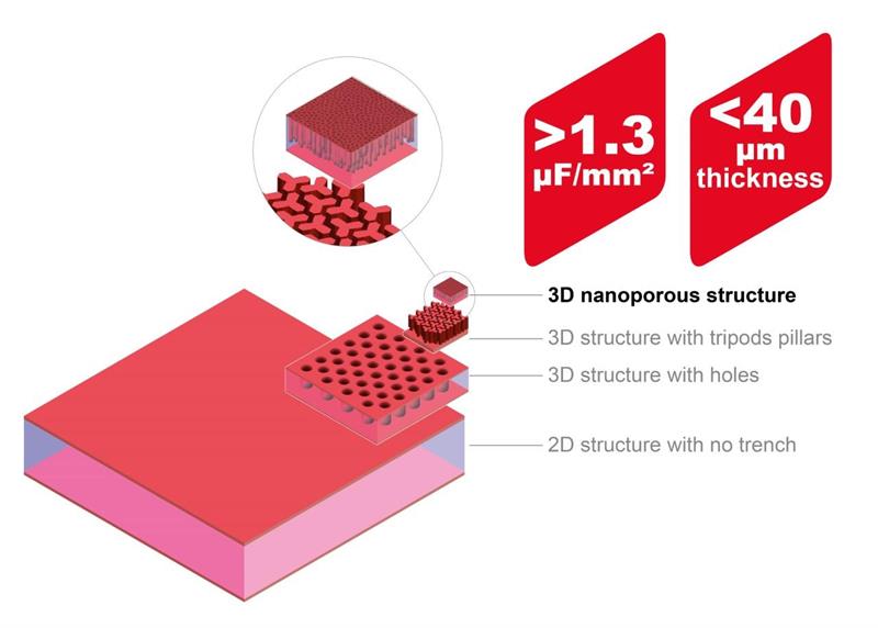
Murata has developed a silicon process technology capable of fabricating silicon capacitors with a density of 1.3 µF/mm².
Intended for the mobile and high-performance computing (HPC) markets these devices have an extremely low ESL (few pH) and low ESR (few mΩ) which support the high performance of new power distribution networks (PDN) that require low impedance over a wide frequency bandwidth.
As digital ICs evolve to offer more features at lower voltages, resolving issues like noise and voltage fluctuation is critical, so with its <40 µm profile chip designer engineers will be able to embed the silicon capacitor into the package as close to the active die as possible, minimizing the current’s effective path length and reducing parasitics.
These multi-terminal devices satisfy the various SoC and microprocessor design requirements for multiple terminal capacitor networks. Replacing conventional monolithic ceramic capacitors with multi-terminal silicon devices reduces the total quantity of capacitors required on the board significantly and will help to improve the overall compactness of the end design.
Fewer capacitors will also result in total savings in both bills of materials and mounting costs.
The Internet of Things (IoT) modules are revolutionizing and improving the way we work with wireless systems in the industrial environment. IoT modules come with a wide range of wireless technology standards, and they provide a variety of features that can impact the success of IoT applications. The fundamental duty of any IoT module is to connect anything to wireless networks. Wireless sensor networks are one of the classic examples of an IoT system. They are the wireless networks that monitor physical or environmental conditions and pass their data through the network to the central location for analysis and processing. The wireless technologies used in IoT modules can range from 5G, 4G, and 3G cellular solutions to Bluetooth and LoRa. IoT modules are useful in industrial sensor-based applications, automotive applications, intelligent road systems, enterprise applications, and many more intelligent systems.
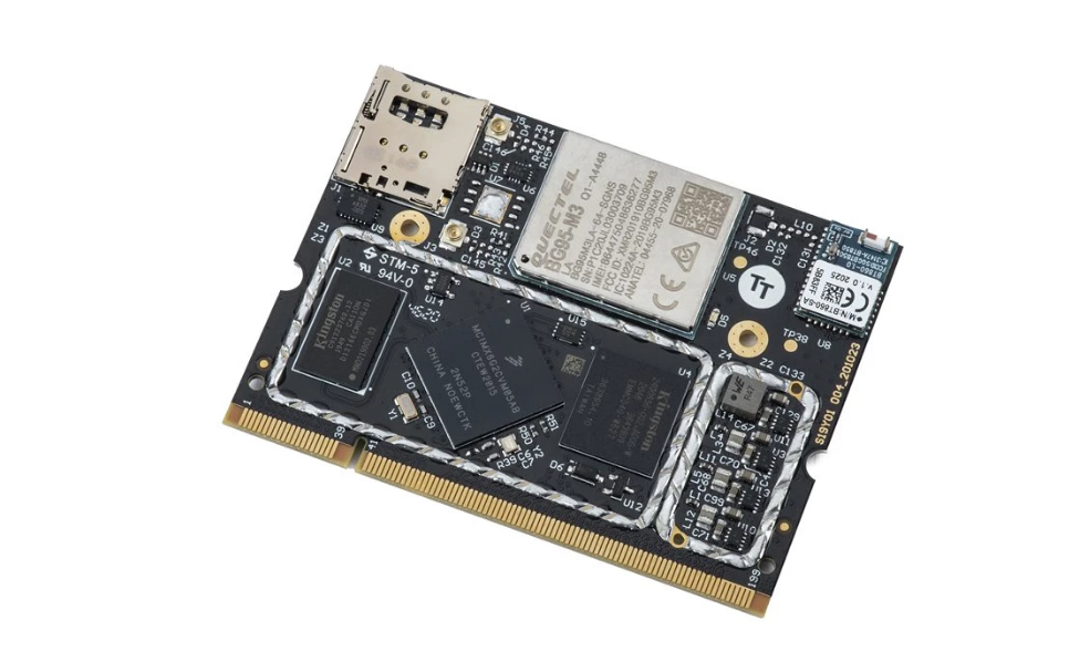
Latest IoT embedded modules are system on a module (SOM), a board-level circuit that integrates a system function in a single module. SOMs are highly suitable for connected IoT applications. TT Electronics recently launched the new S-2CONNECT Creo SOM, a robust, scalable, and cost-effective embedded system-on-module platform for rapid IoT deployment. It is the perfect solution for building wireless systems that deal with real-time sensing and positioning data.
According to the TT Electronics team,
“The system-on-module board is designed for engineers, programmers and developers who are charged with reducing R&D risk and fast-tracking their IoT applications development using a pre-certified system-on-module (SOM) board with cellular connectivity.”
The board features a powerful ARM Cortex-A7 processor with embedded Linux OS, 4GB flash memory, 256MB RAM, and a TPM (Trusted Platform Module) integrated security cryptoprocessor that helps you with generating, storing, and limiting the use of cryptographic keys. Besides, the SOM consists of an eSIM and 3FF micro SIM-card holder with an optional cellular connectivity subscription. The SOM, moreover, supports a wide range of interfaces for connecting peripherals such as Bluetooth, GNSS for positioning, and serial interfaces. This flexibility makes it suitable for various applications such as automation, asset tracking, mobile healthcare, and broader industrial IoT.
The highly integrated SOM solution provides the following benefits for IoT applications:
Ready to use advanced SOM
Access to the latest technology
Reduce R&D Risk
Accelerate development and time to market
Improved efficiency
Reduced carbon footprints
Enabled data-led business decisions
No need for unnecessary maintenance
The company says:
“To meet the rising demand for connected applications, speed to market is critical and the right development tool can accelerate the process. Even experienced developers and integrators can benefit from solutions that provide the hardware, software, firmware, connectivity and cloud-based services that will reduce time-to-market,” commented Kjell Karlsson, Managing Director at TT Electronics.
“In addition, the connectivity landscape is changing and as networks move towards switching off and sunsetting their 3G and 2G infrastructure, the S-2CONNECT Creo SOM has been designed with future-proof LTE Cat M1 and NB-IoT technology to give customers confidence in a solution that will stand the test of time.”
The S-2Connect series can be found here. An online software development kit (SDK) is also available for developers, and an evaluation kit to complement the S-2CONNECT Creo SOM was set to in summer 2021.
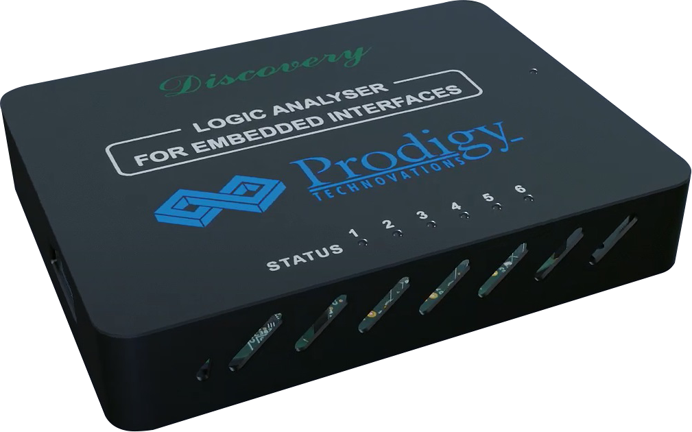
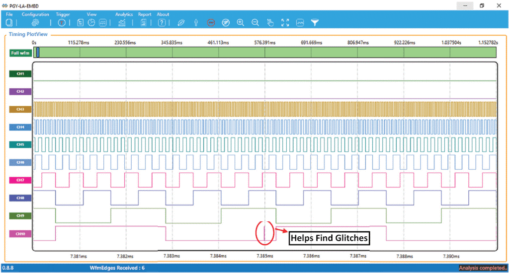
We have already seen several logic analyzers, but an Indian startup, Prodigy Technovations, the leading provider of innovative protocol analysis solutions, has launched a Logic Analyzer for Embedded Interfaces. The Discovery series logic analyzer, also identified as PGY-LA-EMBD, offers a Logic analyzer plus Protocol analyzer in a single product. Building a robust embedded system requires a lot of debugging to make it successful. With PGY-LA-EMBD, the process of capturing and debugging digital signals becomes even more effortless than ever. Together with a small form factor and an easy-to-use GUI, the Discovery series logic analyzers are well suited for hobbyists, small engineering teams, and startup enthusiasts.
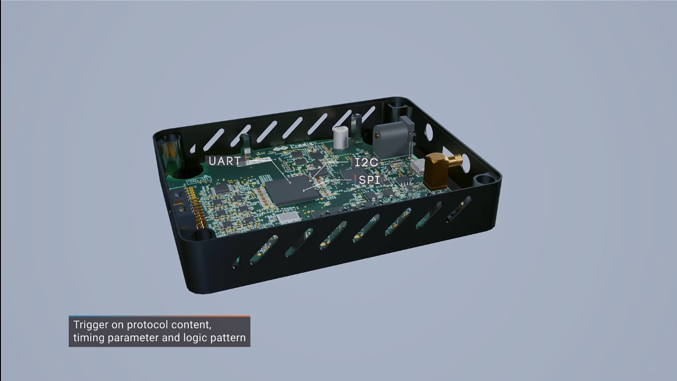
“Current generation embedded designers need to collect data from multiple interfaces such as I2C, SPI, UART, I3C, SPMI and RFFE and process it to achieve optimal performance of their designs. Embedded design teams need to take timely action to meet the intended objectives of the product,” says Prodigy Technovations on the product page. “PGY-LA-EMBD simultaneously decodes I2C, SPI, UART, I3C, SPMI and RFFE bus and displays the protocol activity with timestamp information. PGY-LA-EMBD is an ideal instrument to debug the hardware and embedded software integration issues and optimize the software performance.”
Features of Discovery series logic analyzer
The Discovery series logic analyzer provides a sampling speed of 1 GS/s on all of its channels. In addition to that, it comes with a state speed of 100MHz (synchronous capture). Discovery series logic analyzers can perform simultaneous protocol analysis of I2C, SPI, UART, I3C, SPMI and RFFE interfaces in embedded system designs. With this functionality, the user can simultaneously capture data from all the protocols and view them in a time-correlated view.
Discovery series logic analyzers provide advanced triggering capabilities. These include Auto, Pattern, Protocol awareness (UART, SPI, I3C, SPMI, RFFE and I2C), and timing (pulse width and delay). PGY-LA-EMBD also supports smart continuous streaming of data to the HDD/SSD of the user’s PC through a USB3.0 interface.
PGY-LA-EMBD supports logic levels between 1.2V and 5V. It supports external triggers through an SMA connector and also has a connector for a flying lead probe cable. The status LEDs on the top indicate different conditions such as Trigger found, Trigger set, Capture start, and Capture Stop. Logic analyzers have dimensions of 140x100x35mm and weigh 200 grams in total.
A look into the software part of Discovery series logic analyzer
The software interface for the Discovery series logic analyzer is simple and to the point, making the configuration very easy. The interface displays all the information on a single page about all the connected input channels. Furthermore, it gives the users the flexibility to select sampling rates which allows them to investigate glitches in their designs. Users can capture glitches of up to 1ns with the Timing PlotView.
Video
After capturing and analyzing the data, the user can export the report in either CSV or PDF format. The protocol activity window gives system-level insight to the design team. There are separate decode windows for each interface to provide better insights.
Discovery series logic analyzer retails for $1500. To learn more about it, you can visit the product page or request a demo before buying one.
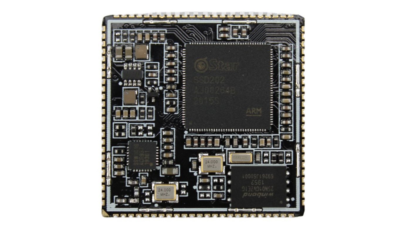
We have already seen several modules coming to the market by Seeed Studio that was based on the SSD202 SoC, which integrated Arm Cortex-A7 processor core running at a clock frequency of up to 1.2GHz. Since this SoC is widely used in smart display applications, Seeed Studio has introduced yet another ultra-small system on module (SoM), IDO-SOM2D02-V1-2GW SoM, designed with 128MB DDR3 RAM and 2GB NAND flash storage.
With the small form factor, the system on module supports Wi-Fi communication through a dedicated Sigmaster Wi-Fi chip, SSW101B that can wirelessly transmit data over 500 meters in open space. This gives the user high performance for several wireless communication IoT and smart display-based applications.
“This SoM has a single-sided layout which means the back of the PCB is completely flat and has no traces. This helps to get rid of any interference when using this board with a carrier board.”
Specifications:
CPU: SigmaStar SSD202 SoC integrated Arm Cortex-A7 dual-core processor, clocked up to 1.2GHz
Video Processor: Support for maximum resolution of 1920×1080 at 60fps decoding, H.265/HEVC Decoder, I/P/B slices
RAM: 128MB DDR3 memory
Storage: 2GB SPI flash storage
Operating system: Linux OS
Wireless network: Sigmaster Wi-Fi chip (SSW101B) capable to transmit over 500 meters in open space
Designed for smart displays, IoT gateways, and smart homes, it comes with support for audio and video interfaces. Audio support has a sampling rate of up to 48KHz giving it better audio quality and processing capabilities. Video support has output support of 1920×1080 at 60 frames per second, signifying the use-case for smart home applications.
For more information on the product, head to the official product page where it is priced at $15.00.
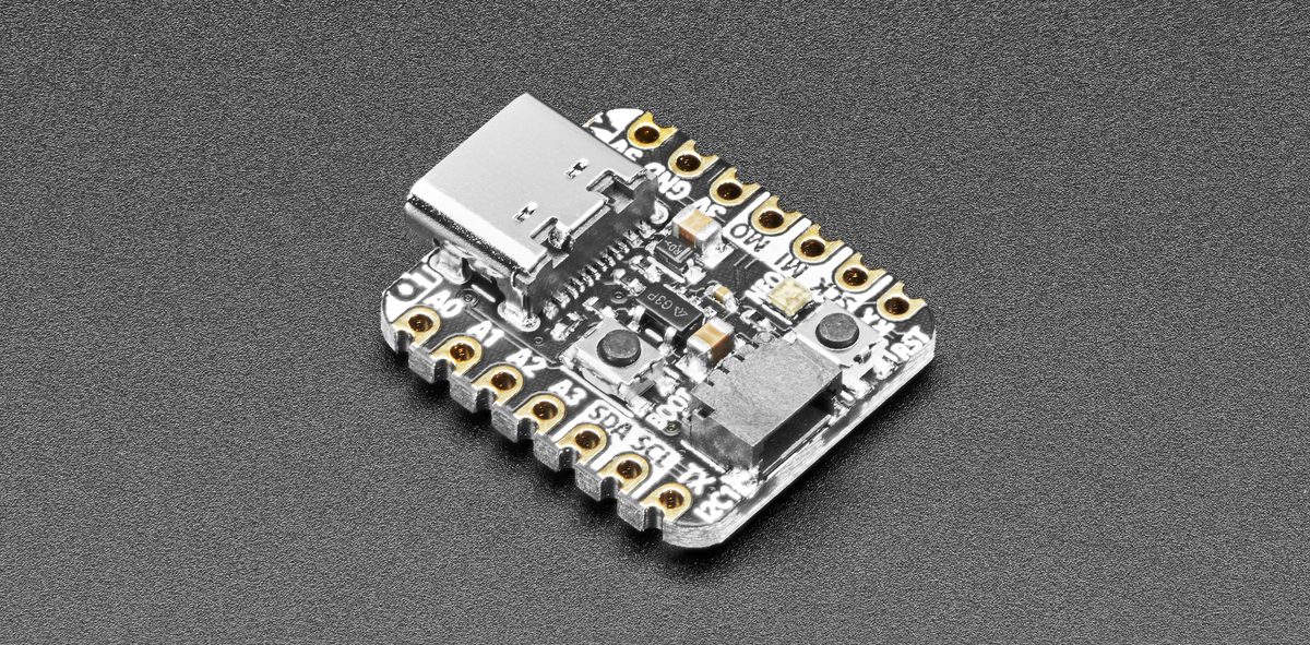
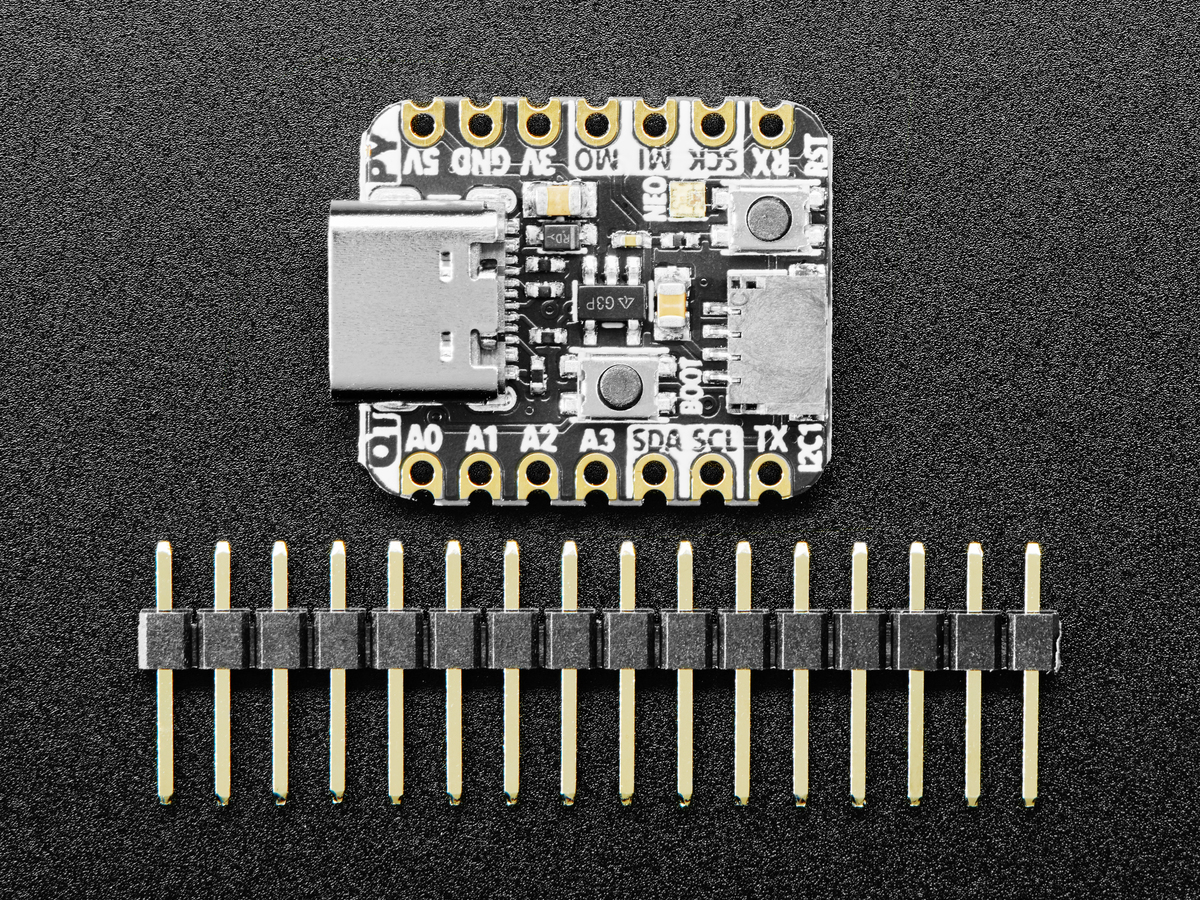
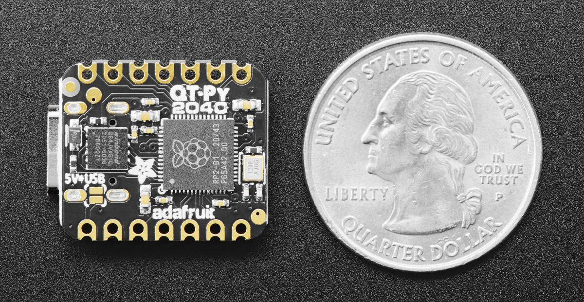
With the growing popularity of the Raspberry Pi’s RP2040 and its powerful features, many third-party manufacturers have come up with hardware based on this chip, such as the Adafruit’s Feather RP2040, ItsyBitsy RP2040, and Pimoroni Tiny2040. The company has turned its attention to bringing the same chip to a new form factor, Adafruit QT Py RP2040, the latest Adafruit tiny board incorporating the Raspberry Pi RP2040 microcontroller. It is twice as fast as the original QT Py and has significantly more storage memory.
Adafruit QT Py RP2040 is a compact board with dimensions of 21.8mmx 17.8mm and a weight of 2.2 grams. Hence, this makes it ideal for wearable applications like fitness trackers and watches. The board comes with a USB interface, which is compatible with all operating systems. Power, data, and programming are all accessible through the USB Type-C connector. This connector helps in incorporating it into small projects like wearables as a reversible connector. Hence, making it easier to access and user-friendly. Many USB HID devices, such as mouse/keyboard shortcuts, and MIDI, are powered by the board.
Speaking more about the hardware design, the Adafruit QT Py RP2040 has two push buttons on the topside: boot and reset, for quick restarts. The addition of these buttons avoids unplugging and replugging to reload the code. It also features a built-in NeoPixel RGB LED on the top of the board, which serves as a status indicator and notifies us when our code has issues.
Technical Specifications of Adafruit QT Py RP2040
Turning the board over, besides the 264KB of storage offered by the RP2040, the board also has an 8MB SPI flash memory to store project files and CircuitPython/Micropython codes. While using C/C++, you receive the whole flash memory. While using Python, you get the remaining 7MB for storing code, files, images, fonts, etc.
However, unlike SAMD21-based QT Py, this QT Py offers 13 GPIO pins, including four 12-bit ADCs, two I2C channels, and two SPI and UART peripherals. Additionally, it has PWM output on every IO pin for servos, LED’s, etc, and 6 GPIO in consecutive order for PIO compatibility. It has also got a 3.3V pin, a powerful voltage regulator capable of providing 600mA of power to the onboard electronics.
The highlight of QT Py RP2040 is the Stemma QT connector located opposite the USB C port.
“STEMMA is a plug-and-play board and sensor system that lets you quickly plug together various devices and accessories. Including OLEDs and inertial measurement units, without any soldering! Use any SparkFun Qwiic boards! Seeed Grove I2C boards will also work with this adapter cable.”
The Pimoroni Tiny 2040 and Adafruit QT Py RP2040, include a dual-core Cortex-M0+ processor running at 125MHz, a USB-C port, two buttons, several I/O ports, and all of the Raspberry Pi RP2040’s features. CNX Software’s post has brought to our attention that both the boards are almost similar with the same specifications and functionalities, except for the I/O’s.
Programming on the Adafruit QT Py RP2040
In terms of programming, you can program this board like the pico or any other RP2040 board. It is C/C++ compatible and comes with official MicroPython and CircuitPython ports. Adafruit provides more intensive support for CircuitPython, thus it is preferred for QT Py RP2040 as well. However, there is no Arduino core support for the chip on this board.
The board costs $9.95, but it is temporarily out of stock. To know more about the Adafruit QT Py RP2040, you can visit the product page. Images and technical specifications have also been taken from the Adafruit store’s product page.
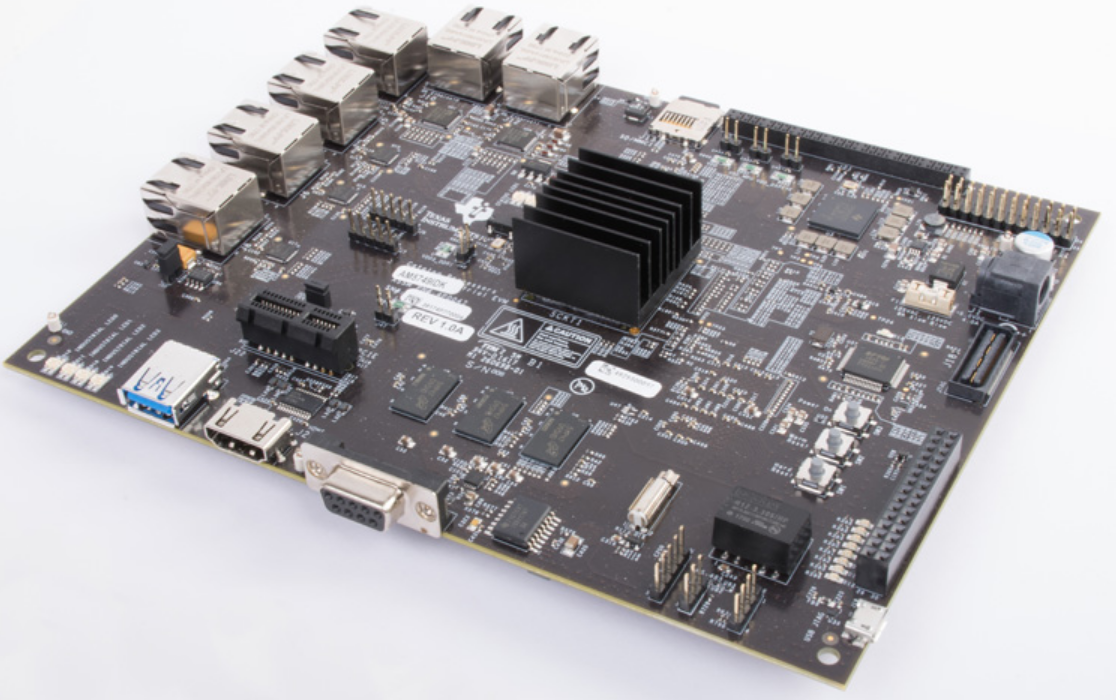
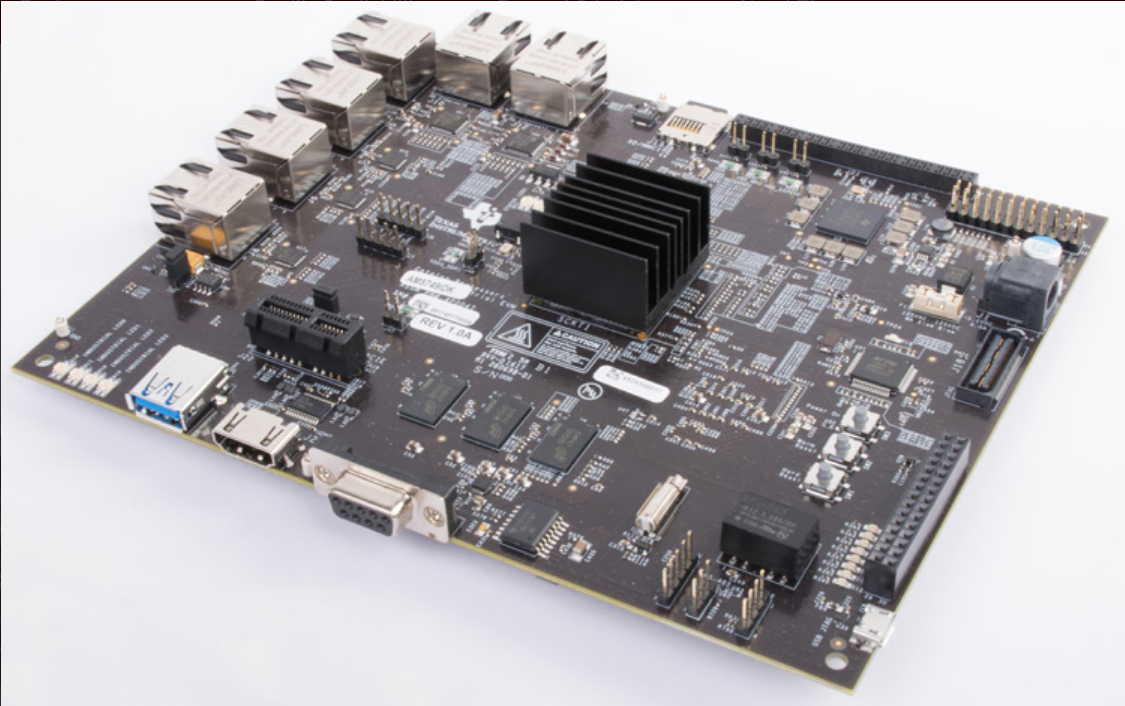
This reference design demonstrates how to use TI Deep Learning (TIDL)/Machine Learning on a Sitara AM57x System-on-Chip (SoC) to bring deep learning inference to an embedded application. This design shows how to run deep learning inference on either C66x DSP cores (available in all AM57x SoCs) and Embedded Vision Engine (EVE) subsystems, which are treated as black boxed deep learning accelerators on the AM5749 SoC.
This reference design is applicable to any application that is looking to bring deep learning/machine learning inference into an embedded application. Customers looking to quickly get started with a deep learning network or to evaluate their own networks performance on an AM57x device will find a step-by-step guide on how to use TIDL available as part of TI’s free AM57x Processor SDK.
Features
Embedded deep learning inference on AM57x SoC
Performance scalable TI deep learning library (TIDL library) on AM57x using C66x cores only, EVE subsystems only, or C66x + EVE combination
Performance optimized reference CNN models for object classification, detection and pixel-level semantic segmentation
Full walk-through of TIDL development flow: training, import and deployment
Benchmarks of several popular deep learning networks on AM5749
This reference design is tested on AM5749 IDK EVM and includes TIDL library on C66x core and EVE subsystem, reference CNN models and getting started guide
After the launch of the cheapest Raspberry Pi’s single-board computer, Raspberry Pi Zero, we have seen several alternatives coming to the market. With the same form factor and minimalistic design, this board integrates an Amlogic S905Y2 SoC with quad-core Arm Cortex-A53 processor core running at a clock frequency of 1.8GHz. Some similar alternatives include the popular Banana Pi M2 Zero that came with Allwinner H2+ SoC but the clock frequency of Radxa Zero outperforms all these alternatives.
With the same form factor, the device comes with a rich set of physical connectivity through 40-pin GPIOs, a USB 2.0 Type C OTG, and one USB 3.0 Type C host. Along with this, the small hardware also supports HDMI 2.1 for video output at 4K resolution at 60 frames per second. On the wireless connectivity, similar to Raspberry Pi Zero W, Radxa Zero also supports WiFi4/BT4 or WiFi5/BT5 depending on the variant.
Features of Radxa Zero
CPU: Amlogic S905Y2 SoC with quad-core Arm Cortex-A53 processor core @ 1.8GHz
GPU: Mali G31 MP2
RAM: LPDDR4 512MB/1GB/2GB/4GB
Flash storage: eMMC 5.1 flash storage of 8/16/32/64/128GB with MicroSD up to 256GB
Wireless connectivity: WiFi4/BT4 or WiFi5/BT5
HDMI: Micro HDMI, HDMI 2.1, 4K@60 HDR
Video: H265/VP9 decode 4Kx2K@60
Peripherals: 1x USB 2.0 Type C OTG, 1x USB 3.0 Type C host, 40Pin GPIO, ADC/UART/SPI/PWM
Given the high performance on such a small board, the manufacturer has designed this with Mali G31 MP2 GPU and integrated RAM options (LPDDR4 512MB/1GB/2GB/4GB). When it comes to choosing an SBC that can deliver high performance along with low cost, then this can be a better alternative as this supports a maximum of 4GB LPDDR4 RAM which is 8x more than the Raspberry Pi Zero W. But it is important to note that, this comes with a drawback if in case you plan to use Raspberry Pi HATs, then this won’t be able to support it.
Radxa Zero v/s Rasberry Pi Zero
When it comes to storage, the Radxa Zero comes with eMMC 5.1 flash storage of 8/16/32/64/128GB and an optional MicroSD card that is expected to support storage up to 256GB. The board adds on with a cryptographic accelerator that performs computationally intensive cryptographic operations. The hardware supports Android 9, but since the manufacturer has already done Armbian booting, it will be the official OS.
The board starts from $15.00 for 512MB LPDDR4 RAM with WiFi4/BT4 and goes up to $45.00 for the 4GB LPDDR4 RAM with 16GB eMMC, WiFi5/BT5 variant. More details are available on the Radxa community page.
As the name suggests, the bypass diodes allow the current to bypass a device or equipment under certain conditions. The conditions of bypass may include the faulty or open-circuited device etc. In solar panels, the bypass diodes come into action when they become faulty or open-circuited or in other words become underrated compared to other adjacent solar panels.
The bypass diodes are connected in reverse-parallel configuration with the solar panel. The solar cells or panels are connected in series to ascertain a voltage level. The bypass diodes installed in reverse-parallel configuration to each cell allow current supply in case any of the adjacent solar cells becomes unavailable. The reverse-parallel configuration does not affect the output of the solar cell and the bypass diode is connected to a group of cells rather connecting across each cell which becomes costly.
Construction and Working Principle of Solar Cell
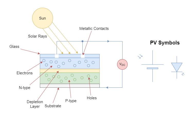
The solar cell is basically a semiconductor device and has layers of semiconductor materials. Just like a PN junction diode, the solar cell is made of P-type and N-type layers. These layers are formed by doping with materials having excess or deficiency of electrons. The layer having excess electrons is made of N-type semiconductor and the layer having deficiency of electrons or excess of holes is made of P-type semiconductor. The combination of these layers enables the silicon wafer to become light-sensitive and produces electric energy across its terminals upon striking of photons/ light. A number of such silicon wafers are connected in a series-parallel combination to obtain a cell of significant open-circuit voltage and this comprises a solar cell.
The solar cells are connected to each other through metallic strips to guide the flow of current towards the output. The light falling upon cells gives energy to electrons of semiconductor material and free them from atomic bonds. The electrical paths are established using semiconductor materials to collect current from each semiconductor wafer towards output, collectively. The solar cells are connected with each other on the surface facing the Sun. The sun-facing surface is made anti-reflective in order to absorb most of the sunlight falling upon it. The two electrical contacts (+ & -) obtained from the solar panel are either connected to the load or other panels to expand the capacity of the overall solar system. The positive terminal is normally obtained from the front surface and the negative terminal from the back surface of a solar cell.
Figure 1: The Solar Cell construction under the Sunlight and its symbols
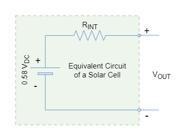
The voltage produced by a single solar cell normally ranges from 0.5 to 0.6 Volts (DC). The voltage produced by a solar cell depends on the construction and configuration of the solar cell. However, the magnitude of the current produced upon connection of load depends majorly on the photons striking on the surface of the solar panel. Normally, the voltage remains nearly constant whereas the current is considered to be proportional to the size of the cell and the intensity of light falling upon it. The solar cells may vary to other connected solar cells due to the manufacturing process and this can be modeled as internal resistance in conjunction with the solar cell. The equivalent model of a solar cell or photovoltaic (PV) cell is shown in the following figure.
Figure 2: The equivalent circuit of a Solar Cell
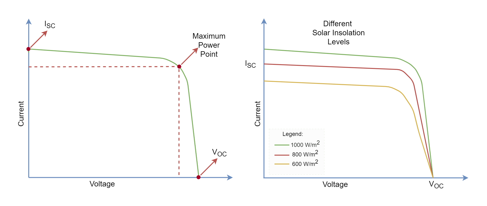
Photovoltaic (PV) Characteristics
The photovoltaic solar cells produce DC power when exposed to sunlight. In the absence of load (IOC = 0), the voltage produced is maximum and termed as open-circuit voltage (VOC). The open-circuit voltage (VOC) is normally in the range of 0.5 to 0.6 Volts DC and such a voltage is quite less compared to standard battery voltage i.e. 1.5 Volts. The series connection of multiple cells can increase the open-circuit voltage just like normal batteries.
The maximum current produced by the solar cell is dependent on sunlight absorption. Under certain sunlight exposure, the maximum current is produced upon shorting the terminals and is called short-circuit current (ISC). However, at this operating point, the open-circuit voltage has reduced to zero and, as such, the output voltage is dependent very much on the load current. The output voltage (VO) increases from 0 to VOC as the output current decreases from ISC to 0.
Figure 3: I-V Characteristic of a typical Solar Cell and I-V Characteristics at different Insolation levels
The output current or power is proportional to the intensity of sunlight absorbed by the front surface of the photovoltaic. For example, under cloudy weather, the sunlight striking on the front surface may reduce the output current or power but, still, it may produce a full output voltage. Brighter sunlight, not the temperature, can provide a heavy load current requirement of a load connected to it. However, there exists a maximum limit of the current that can be produced i.e. IMAX which can be delivered to the load and depends majorly on the size of the photovoltaic.
The selection of diodes for the solar cells merely depends on the maximum deliverable current (IMAX) of the photovoltaic. It depends on:
The surface area of the cell
Sunlight
Type of semiconductor used
The efficiency of conversion into electric current
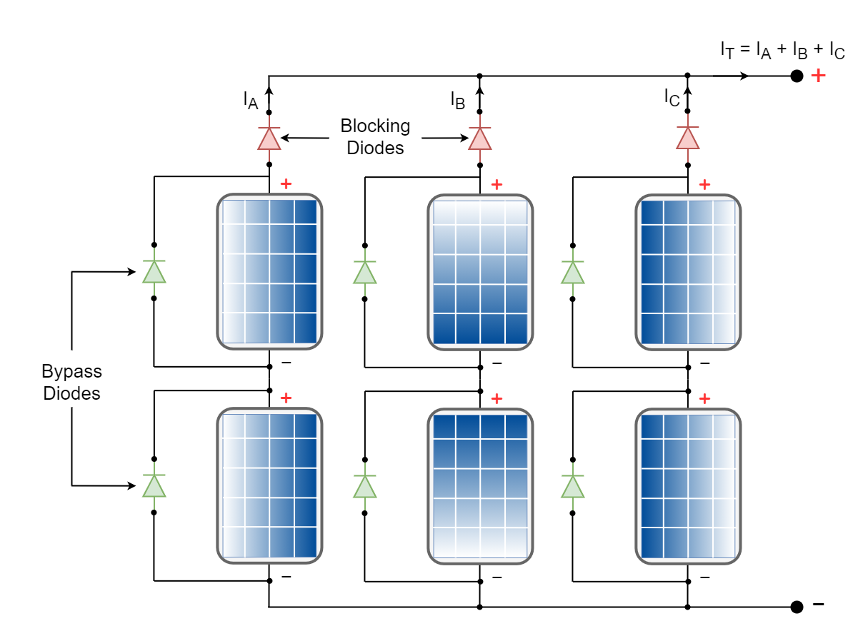
Usage of Diodes in Photovoltaic Arrays
A photovoltaic array consists of solar panels connected in series and parallel configuration. A series combination helps in attaining a higher open-circuit voltage whilst a parallel combination provides a higher output current. The diode is a unidirectional device which means that it allows the flow of current only in one direction. The blocking diodes used in the series branches allow the branch currents to flow from solar cells/ panels to the output only. In absence of blocking diodes, the branches with higher voltages may contribute/ supply current to low voltage branches causing loss and heating. A damaged cell or partial shading can lead to such a condition. However, blocking diodes block the current flow from other branches to branches with such solar panels.
Bypass Diodes
The bypass diodes are placed in reverse-parallel arrangement with the solar cell or panel. As we know that in the series branch the same current flows through each series element. In a photovoltaic array, a solar panel output may weaken due to deterioration or partial shading which may reduce its current capacity compared to the current produced by efficient and fully exposed to sunlight solar panels. The current produced by efficient and exposed solar panels may overdrive the inefficient solar panel causing overheating and burning. However, a bypass diode becomes forward-biased under such conditions, and current flows through bypass diodes rather than passing through weakened/ damaged solar panels. The bypass diode is placed parallel to the solar panel whereas the blocking diode is placed in series with solar panels.
Similar diodes can be used as bypass or blocking diode but they both serve different purposes and rating of these diodes depend on the IMAX of the series branch.
Figure 4: The PV array with bypass and blocking diodes
In the above figure, the green color diodes placed in parallel to solar panels are bypass diodes. They serve the purpose of a low resistance path and should have the capability to safely handle the rated current. The red color diodes are blocking or isolation diodes and they ensure that current flows from solar panels to the output only towards the external load. This is to prevent flow of generated current from parallel branches to other branches of the same array which has shaded/ weakened solar panels. Also preventing, drainage of charged batteries by supplying current to a solar array at the night. The blocking diodes are used in each parallel branch of a photovoltaic array.
The conventional diode and Schottky diode can be used as a bypass and blocking diode. Moreover, they are available in a wide range of ratings and can be selected as per photovoltaic array rating. Moreover, the voltage drop of a conventional diode is around 0.7 Volts and of Schottky diode is around 0.4 Volts. The less voltage drop of the Schottky diode makes it more suitable for usage in photovoltaic arrays as bypass and blocking diode. The Schottky diodes cause less voltage drop in a series branch, leading to an efficient array with less power dissipation in blocking diodes.
The manufacturers of photovoltaic panels fabricate the bypass and blocking diodes inside the solar panels to keep the external circuitry simple.
Conclusion
The solar cells are made of semiconductor layers having an excess of electrons (N-type) and deficiency of electrons (P-type).
The layers that form the PN junction are sensitive to light/ photons. The light energy is converted into electrical energy by this PN junction forming a solar cell.
The voltage of a solar cell is very low in the range of 0.5 to 0.6 Volts DC and can be increased by adding multiple solar cells in series and may include parallel branches as well. This form of solar cells in series parallel combination makes a solar panel.
The current produced by the solar cells is dependent mainly on the light intensity, surface area, and material used in its fabrication.
The solar arrays are formed by further connecting multiple solar panels in series-parallel combination increasing the covered area with a large number of solar panels.
The series solar panels may face reduced current when any solar panel gets damaged or becomes partially shaded. In such a case, a bypass diode is used to bypass that weakened solar panel to avoid heating and burning of that solar panel.
Similarly, the current may flow from other parallel branches to weakened branches. Especially, at night, the charged batteries may start supplying current towards the solar array. In order to prevent this backward current flow in a branch, a blocking diode is used.
The rating of bypass and blocking diodes depend on the maximum current rating of the solar panel. Both diodes can be the same but serve different purposes.
The Schottky diode has a less forward voltage drop compared to conventional PN junction diode and is more efficient in solar panels.
The bypass and blocking diodes are normally internally connected by the manufacturer to keep the design simple.
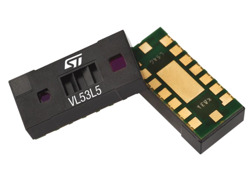
STMicroelectronics VL53L5 FlightSense™Time-of-Flight Mini Depth Camera integrates a SPAD array, physical infrared filters, and diffractive optics (DOE) in a miniature reflowable package. These features allow the VL53L5 to achieve the best ranging performance in various ambient lighting conditions with various cover glass materials. The use of a DOE above the vertical-cavity surface-emitting laser (VCSEL) allows a square FoV to be projected onto the scene. The receiver lens focuses the reflection of this light onto a SPAD array.
The STM VL53L5 FlightSense Time-of-Flight Mini Depth Camera utilizes a direct ToF technology that allows absolute distance measurement, whatever the target color and reflectance. The ToF technology provides accurate ranging up to 400cm, and the 32bit MCU with extra HW accelerator can post-process the histogram and stream ready-to-use depth information at fast speeds (60Hz).
Features
Fully integrated miniature module
Emitter: 940nm invisible vertical cavity surface emitting laser (VCSEL) and integrated analog driver
61° diagonal square system field of view (FoV) using diffractive optical elements (DOE) on both transmitter and receiver
Receiving array of single photon avalanche diodes (SPADs) in both transmitter and receiver apertures
Low-power microcontroller running firmware
6.4mm x 3.0mm x 1.5mm Size
Fast, accurate distance ranging
Parallel multi zone output; either 4×4 or 8×8 separate regions of interest (ROI)
Up to 400cm ranging
60Hz frame rate capability
Histogram processing and algorithmic compensation minimizes or removes impact of cover glass crosstalk
Fully autonomous device with on-board histogram and ranging processing running on ST in-house 32Bit MCU
Dynamic crosstalk compensation for fingerprint smudge via latest patented ToF techniques
Easy integration
Flexible power supply options, single 3.3V or 2.8V operation or combination of either 3.3V or 2.8V AVDD with 1.8V IOVDD
Compatible with wide range of cover glass materials
I²C or SPI interface
Low-power pin and two general purpose inputs (GPIOs) for interrupt and synchronization
Full set of software drivers (Linux and Android compatible) for turnkey
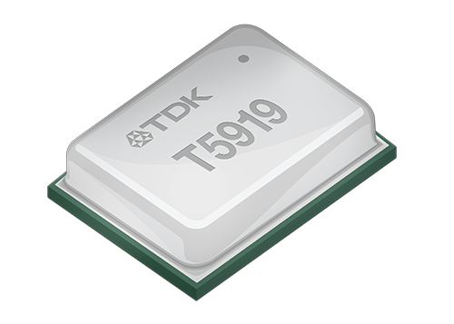
TDK Corporation introduces three new MEMS microphones as part of the SmartSound™ family of products for mobile, IoT and other consumer devices. Each of these high-performance microphones push the boundaries of microphone acoustic performance, providing advanced feature sets with very low power in small package footprints. The SmartSound family of MEMS microphones from TDK are designed for a multitude of applications in a variety of dynamic environments. Our High AOP, high SNR and wide dynamic range microphones are ideal for environments that shift from very quiet to very loud, such as far-field voice pickup barge-in for Smart Speaker applications.
T5919, the world’s first PDM digital output microphone with built-in Particle Ingress Filter (PIF):
The T5919 is a multi-mode, low noise digital MEMS microphone in a small 3.5 x 2.65 x 0.98 mm bottom port package. The PIF filter is embedded in the microphone package, providing protection to particles and moisture. T5919 includes multiple modes of operation: High Quality, Low-Power (AlwaysOn), and Sleep. The T5919 microphone boasts high SNR in all operational modes. The microphone maintains 135 dB SPL AOP in High Quality Mode and 120 dB SPL AOP in Low-Power mode.
T4086, an ultra-small analog output MEMS microphone:
The T4086 analog microphone is designed to achieve high SNR and AOP at low power in a tiny 2.75 × 1.85 × 0.9 mm bottom port package to support very space constrained applications/devices.
T3903, a very low power wide dynamic range PDM MEMS microphone:
The low power T3903 enables the transition of microphones from analog output to digital output to support ‘AlwaysOn’ applications in smartphones, tablets, remote controls, smart TVs, Bluetooth headsets, and digital still/video cameras. The T3903 is a multi-mode, low noise, bottom ported MEMS microphone with -37dBFS sensitivity, 66dBA SNR and 133dB AOP in a 3.5 × 2.65 × 0.98 mm package.
“TDK continues its commitment to bringing to market a broad portfolio of disruptive, high performance and innovative SmartSound solutions,” said Omar Abed, GM and VP of microphone business unit at InvenSense, a TDK group company. “By applying several new MEMS technological breakthroughs, we developed microphones designed for a multitude of applications in a variety of challenging and dynamic environments, thus enabling our customers to create a differentiated audio experience.”
The TDK T5919, T3903 and T4086 are available from multiple distributors and are part of a fully compatible and multi-grade SmartSound portfolio of microphone products.