The role of power supply is crucial for electronic circuits because without sufficient power, the circuit cannot function at its optimal level. On the other hand, an exceeded power supply can deteriorate the circuit components by heating effect. There are usually two choices for power supply topologies; Linear Power Supply and Switched Mode Power Supply (SMPS).
The linear power supply is traditionally an old topology, thus it had its presence in the design and architecture of older electronic components. But the new Switched Mode Power Supply topology is preferred over Linear Power Supply for current circuit designs due to its increased efficiency and compact size. However, the SMPS has more components and complex design still its advantages outweighs the linear power supply.
Also, the cost of SMPS was high initially
“but with the birth of the electronic age, component costs have dropped so low that the high raw material content of copper and iron in the linear transformer has made the SMPS technology more cost-effective.”
We saw the introduction of SMPS technologies by Microchip’s A1114 application note, which described the working of SMPS circuits in December 2015. The application note highlights the applications of various SMPS technologies and the design specifications of components for SMPS. It also suggests the factors for consideration while selecting SMPS topologies.
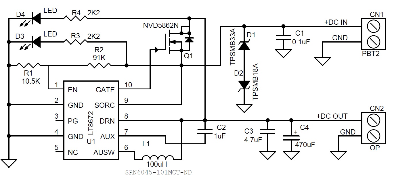
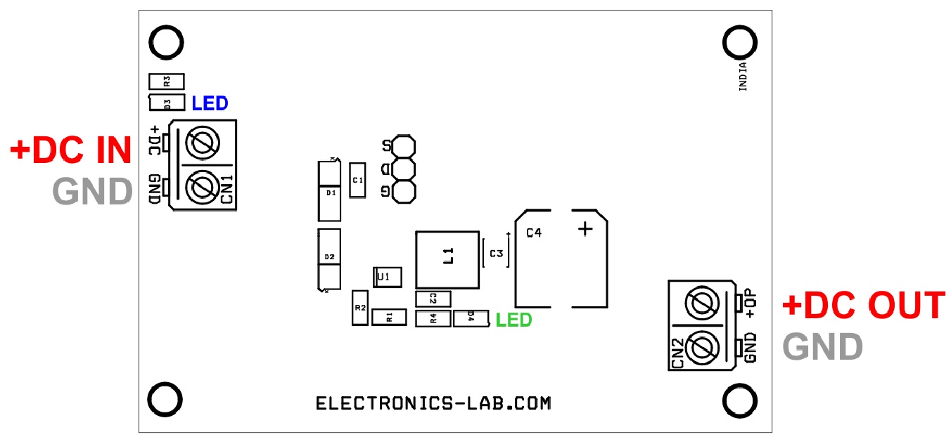
Switched Mode Power Supply Topology
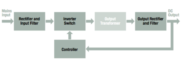
As Switch Mode Power Supply contains a large number of components, thus it needs different stages. Every stage takes care of all the factors necessary for optimal performance. Example: If the input supply is AC, then the input stage has a provision of rectifier and low-pass filter for AC to DC conversion. There is also an inverter stage available for DC to AC conversion by simultaneous switching DC voltage on and off. The rate of switching decides the frequency of the AC output.
We also saw the Open Electronics’ Switched Mode Power Supply known as Torpedo, with a SEPIC configuration. Its circuit structure came with three different stages; Input Stage, Battery Charger, and SEPIC Converter. A transition from battery power to another source without interruptions was one of the unique features of the Torpedo circuit.
Comparison between Linear Mode and SMPS
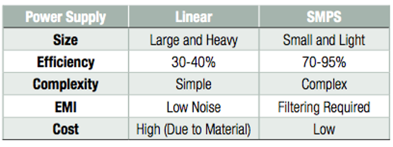
From the above image, it is quite clear that SMPS is preferred over linear mode power supply when design criteria are taken into consideration. Also, the compact size and efficiency also act in favour of SMPS as discussed in the previous sections. Although SMPS outweighs linear mode, the selection of different topologies of SMPS is also a difficult choice. There are various SMPS topologies:
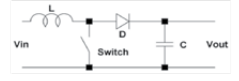
Buck
Generally, Buck topology needs a single inductor for single-phase use cases. But there is a necessity for catalog inductors in the case of robust applications. As the topology comes with an inductor in series and capacitor in shunt, it is ideal for DC to DC conversion. Although buck converters provide high efficiency and power levels with poly-phase topologies, it is not an appropriate choice for use cases where isolation is necessary.
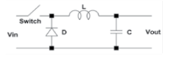
One of the major drawbacks of buck converters is that the input current is always discontinuous which results in larger EMI. However, it can be solved with filter components such as chip beads, common mode chokes and filter chokes. Additionally, one can also build custom inductors for specific cases and for applications that need additional coils for sensing and providing power.
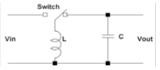
Boost
Boost topology is preferred for non-isolation use cases. It helps in stepping up voltages because of the switch in shunt position with respect to the input voltage. The topology also provides a wide range of catalog options for inductors in boost circuits depending on the functionality requirement. Additionally, the provision for the use of custom inductors helps with the dynamic designing of circuits for various applications.
The power factor variation from the unity value reduces the efficiency of the circuits. Hence, there is a necessity for a power factor correction circuit to bring this value close to one. Boost topology draws continuous current when operating in conduction mode, thus it improves the power factor in case of significant variations.
Buck-Boost
As the name suggests, buck-boost topology is the combination of individual Buck and Boost topologies. Hence, the topology is suitable for both step-up and step-down voltage applications. As the connection of the inductor to the main circuit varies with the switch position, thus the flow of the drive circuit is a bit complex.
This topology is specifically useful for battery applications because the input voltage varies over time but it comes with the drawback of inverting the output voltage.
SEPIC/Ćuk
The SEPIC and Ćuk topologies both utilize capacitors for energy storage along with the two inductors in the circuit. “The two inductors can be either separate inductors or a single component in the form of a coupled inductor.” The step-up or step-down feature makes them suitable for battery applications.
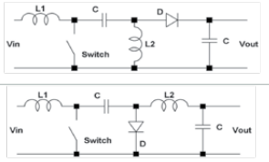
SEPIC topology is preferred over both the Ćuk and the buck-boost due to its non-inverting output. Capacitors in both topologies provide limited isolation, hence it addresses the isolation issue.
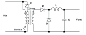
Flyback
Flyback topology consists of a transformer that acts as a storage inductor for providing isolation. The transformer also opens the option for variable voltage by adjusting the turns ratio. Additionally, the use of a transformer creates the possibility for multiple outputs.
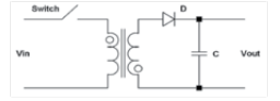
Flyback topology is the simplest and most common of the isolated topologies for low-power applications. Additionally, the flyback transformer avoids the requirement for a separate inductor, thus it is a cost-effective topology.
Forward
The forward topology comes with a transformer along with an extended buck circuit at the output side of the transformer. Hence, it is also known as a transformer-isolated buck converter. Forward circuits are flexible for high current supply due to non-pulsating output current. Thus it is a good choice for applications with excessive current specifications of 15A.
“Like the flyback topology, the forward converter is specifically for lower power applications. While efficiency is comparable to the flyback, it does have the disadvantage of having an extra inductor on the output and is not well suited for high voltage outputs.”
Push-Pull
As seen from the circuit, push-pull topology comes with dual primary windings of the forward topology circuits to build a two-drive winding. Hence, it increases the efficiency as the utilization of the transformer core is optimal than any flyback or a forward converter. Push-pull converters also have a provision of scaling up during high-power requirements.
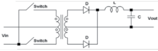
As the use of copper is 50% at an instance, thus it leads to an increase in the copper loss values. For alike power levels, the push-pull circuits feature compact filters with respect to the forward converter. Additionally, the switching functionality is crucial because if both the switches turn on simultaneously. Then it will cause an equal and opposite flux in the transformer, thus reducing the impedance of the circuit. This sudden drop in the impedance value rises the current value exponentially. Hence, there is a potential chance for the damaging of the circuit.
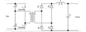
Half-Bridge
The half-bridge topology also features the functionality of scaling up to higher power levels like the push-pull topology. Hence, it also has the same issue of a sudden rise in the current if the switches are on simultaneously. “In order to control this, there needs to be a dead-time between the on-time of each switch. This limits the duty cycle to about 45%. Beneficially, the half-bridge topology switching stresses are equal to the input voltage. This makes it much more suited to 250VAC and PFC applications.”
Resonant LLC
Resonant LLC circuit has a design similar to Half-Bridge topology, it further uses the concept of resonance to cancel the leading and lagging effect. This decreases the switching losses because of the zero voltage switching even if the circuit is in the no-load mode.
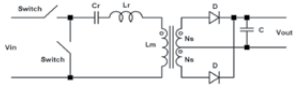
This topology is a very good choice for standby mode power supplies, as the resonant tank circuit requires a continuous supply of energy. The resonant LLC is preferred over both push-pull and half-bridge topologies as it is flexible for a wide range of input voltages. The only drawback to the resonant LLC topology is its “complexity and cost.”
For detailed information on the specifications and parameters of every topology, you can download this pdf file by clicking here.
source: https://www.we-online.com/web/en/electronic_components/news_pbs/blog_pbcm/blog_detail-worldofelectronics_45887.php