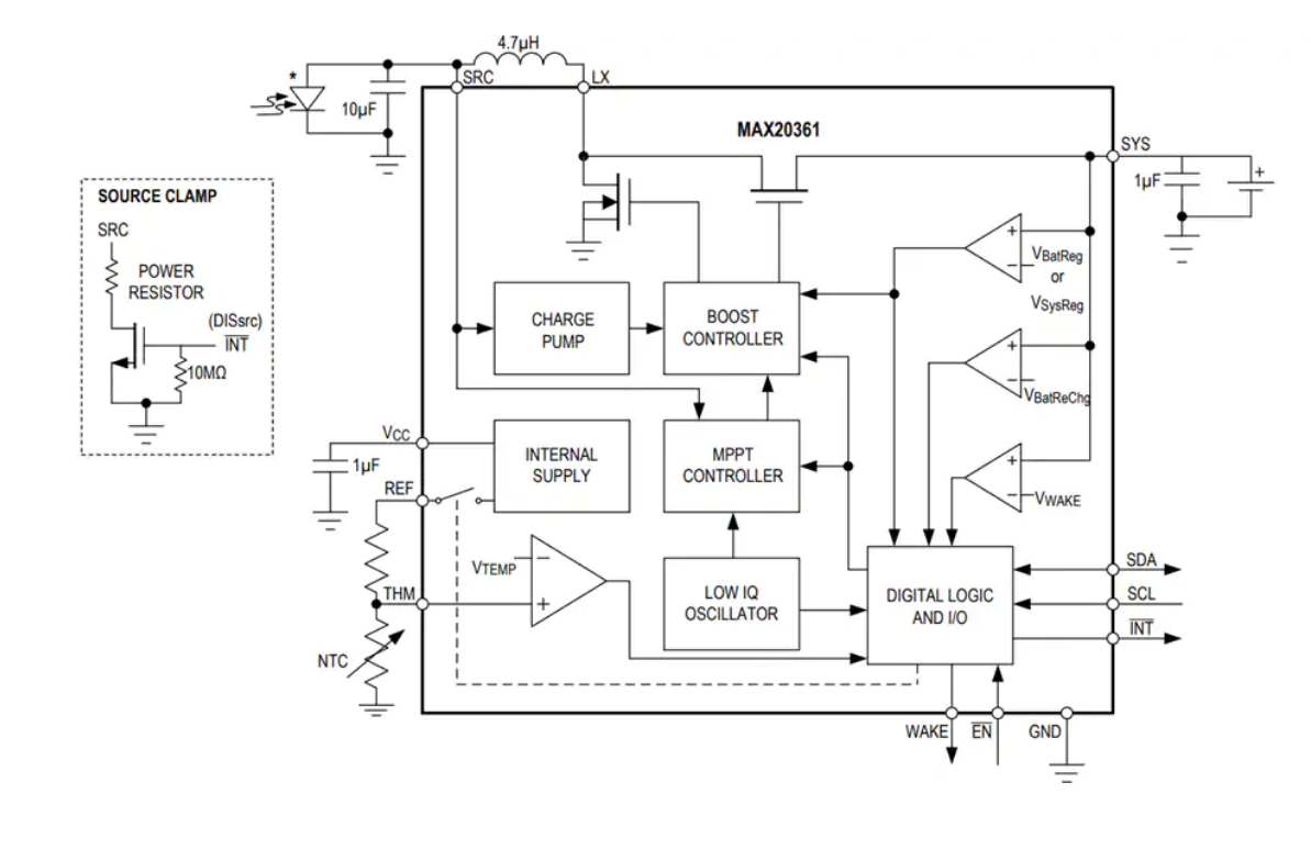
Maxim Integrated MAX20361 Single-Cell/Multi-Cell Solar Harvester is a fully integrated solution for harvesting energy from single-cell and multi-cell solar sources. The MAX20361 includes an ultra-low quiescent current (360nA) boost converter that is capable of starting from input voltages as low as 225mV. To maximize the power extracted from the source, the MAX20361 implements a proprietary maximum power point tracking (MPPT) technique that allows efficient harvesting from 15μW to over 300mW of available input power.
The MAX20361 features an integrated charging and protection circuit that is optimized for Li-ion batteries. This device can also be used to charge supercapacitors, thin-film batteries, or traditional capacitors. The charger features a programmable charging cut-off voltage with thresholds programmable through an I2C interface as well as temperature shutoff.
The Maxim Integrated MAX20361 Solar Harvester is available in a 12-bump, 0.4mm pitch, 1.63mm x 1.23mm wafer-level package (WLP).
Application Circuit
Features
Single-Cell/Multi-Cell Solar Energy Harvester
225mV to 2.5V (typical) input voltage range
Efficient harvesting from 15μW to over 300mW of available input power
86% efficiency at VSYS = 3.8V, ISRC = 30mA
Small solution size
Utilizes small 2016 4.7μH Inductor
Maximum Power Point Tracking (MPPT) technique using fractional VOC method
Programmable fractional VOC regulation point through I2C interface
Battery/supercapacitor charger
Programmable battery termination voltage through I2C interface
Programmable Power Good Wake-Up signal output threshold through I2C interface
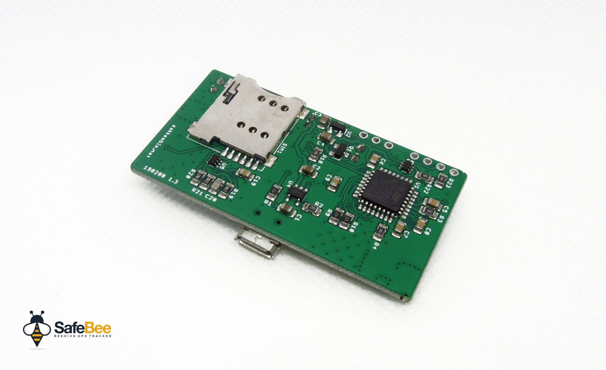
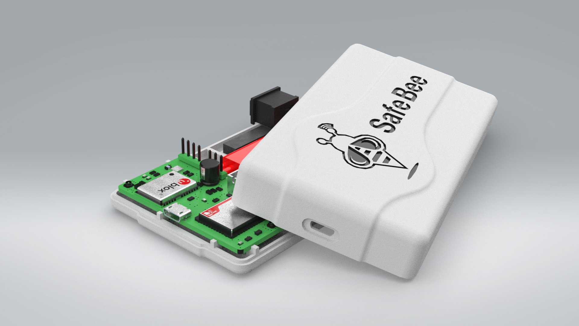
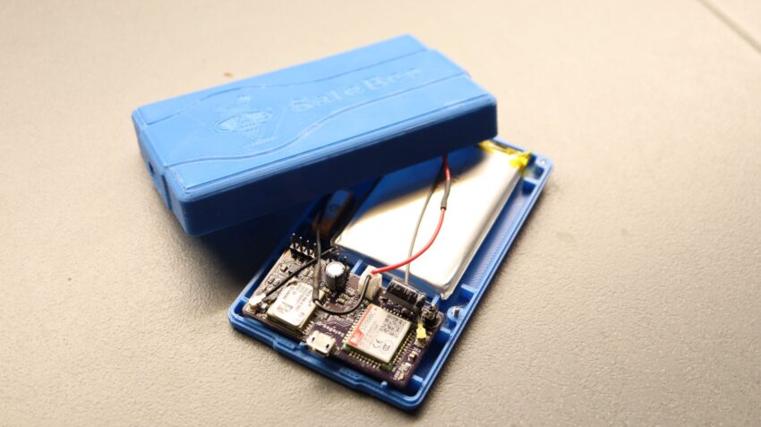
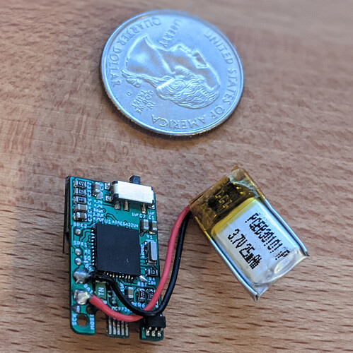
This is an original design of a GPS tracker designed on Elab and it is intended to be used as a security device for beehives, but it is not limited to this. It can be used everywhere a motion-activated GPS tracker is needed, like your car, bike, or even your boat. It is a GPS tracker controlled by simple SMS commands and designed for reliability,low power consumption, and easeof use. It features a MEMS accelerometer that is used to intelligently detect movement and once triggered it will power on the GPS module and will try to acquire the current coordinates. The location details will be transmitted to the owner’s smartphone via a simple SMS and then follow update the coordinates at predefined intervals.
Key Features:
Remote management via simple SMS commands
High reliability – no need to babysit the tracker due to crashes and resets
Long battery life – over 1 year standby on a single charge (2500mAh battery)
3-axis high-sensitivity MEMS Accelerometer
Intelligent Triggering – it will not be triggered by accidental movement
Selectable Trigger Sensitivity Level
Description of Operation
The tracker has 3 main modes of operation, detailed below:
Standby
Ready
Tracking
Standby mode
In standby mode, the GSM and GPS modules are powered down and the microcontroller is in sleep mode, resulting in a current draw of approximately 70uA, mainly by the accelerometer (MMA7660). The accelerometer is used to detect movement caused by a possible thief. If the accelerometer is triggered 1 or 2 or 3 times (depending on the sensitivity level) inside of a 60-second window then the device will enter tracking mode. While in standby mode the tracker will also enter ready mode approximately every 12 hours, triggered by the microcontroller’s internal RTC. This is to check for incoming commands and battery status etc.
Ready mode
The ready mode is entered by the microcontroller’s internal RTC and when the tracker is first powered on. In this mode, the tracker will power up the GSM module and wait for any SMSs to come in and process them. The tracker will stay in ready mode for 5 minutes before returning to standby mode unless an SMS command has instructed the device to enter tracking mode (BEE+TRIGGER).
Tracking mode
Tracking mode is entered when manually instructed to by the BEE+TRIGGER command or after the accelerometer triggers (1 or 2 or 3 movements detect depending on sensitivity level) within a 60-second window, from either standby or ready modes. In tracking mode, the tracker will power up both the GSM and GPS modules and begin to send tracking alert SMSs to the number configured by the BEE+NUMBER command. The device will continue to stay in tracking mode until the BEE+CLEAR command is received or while the accelerometer is detecting movement and/or the GPS module has a lock and the speed is greater than 10KPH. If neither of these conditions is met for 6 minutes then the tracker will send a tracking stopped SMS and return to standby mode, or ready mode if the RTC was triggered within the last 5 minutes.
Power up and Battery Status
In ready and tracking modes if the battery voltage falls below the threshold voltage (3650mV default) then a low battery alert SMS will be sent to the number configured by BEE+NUMBER. Approximately every 30 days (60 RTC triggers) an automated status SMS is also sent to the number configured by BEE+NUMBER.
When power is first applied to the device the tracker will be in ready mode and it will check for incoming SMS and then go to sleep. This is the ideal time to configure the tracker with the BEE+NUMBER number. This is the number that tracking messages, monthly status reports, and low battery alerts will be sent. The phone number is stored in the microcontroller’s FLASH memory and it will be permanently saved, even if battery power is removed. At power-up, the tracker will send a status SMS and also ignore any movement detected by the accelerometer for the first 60 seconds.
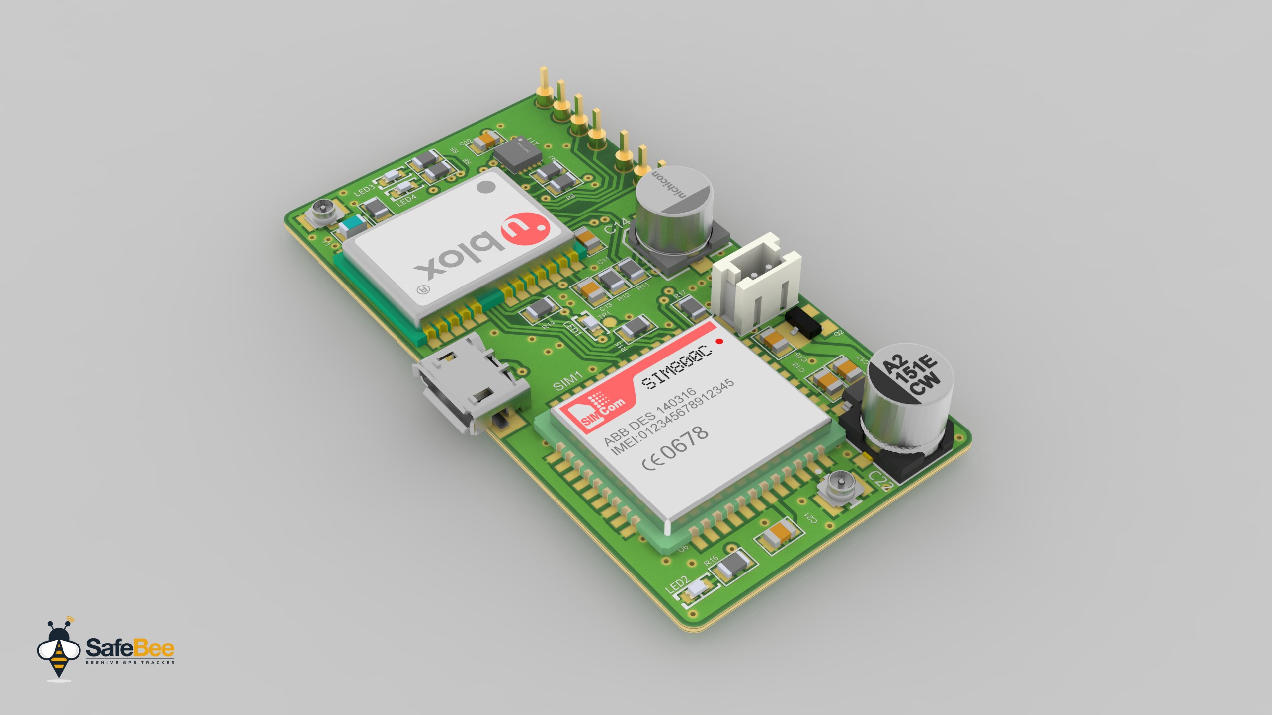
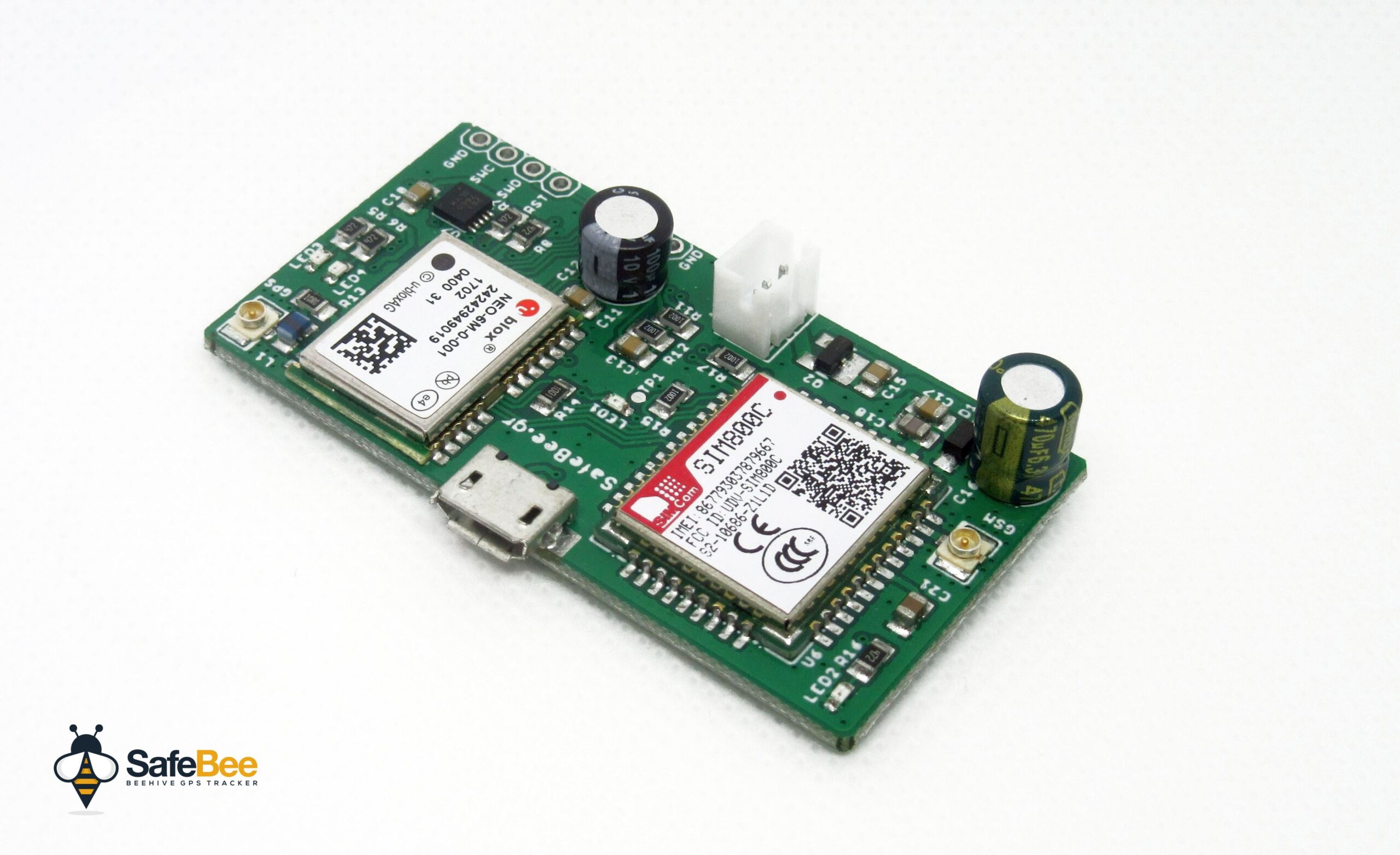
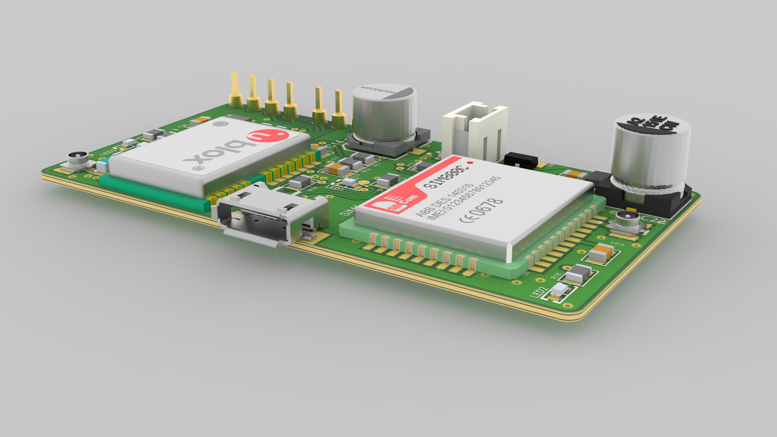
The Hardware
Hover images for details
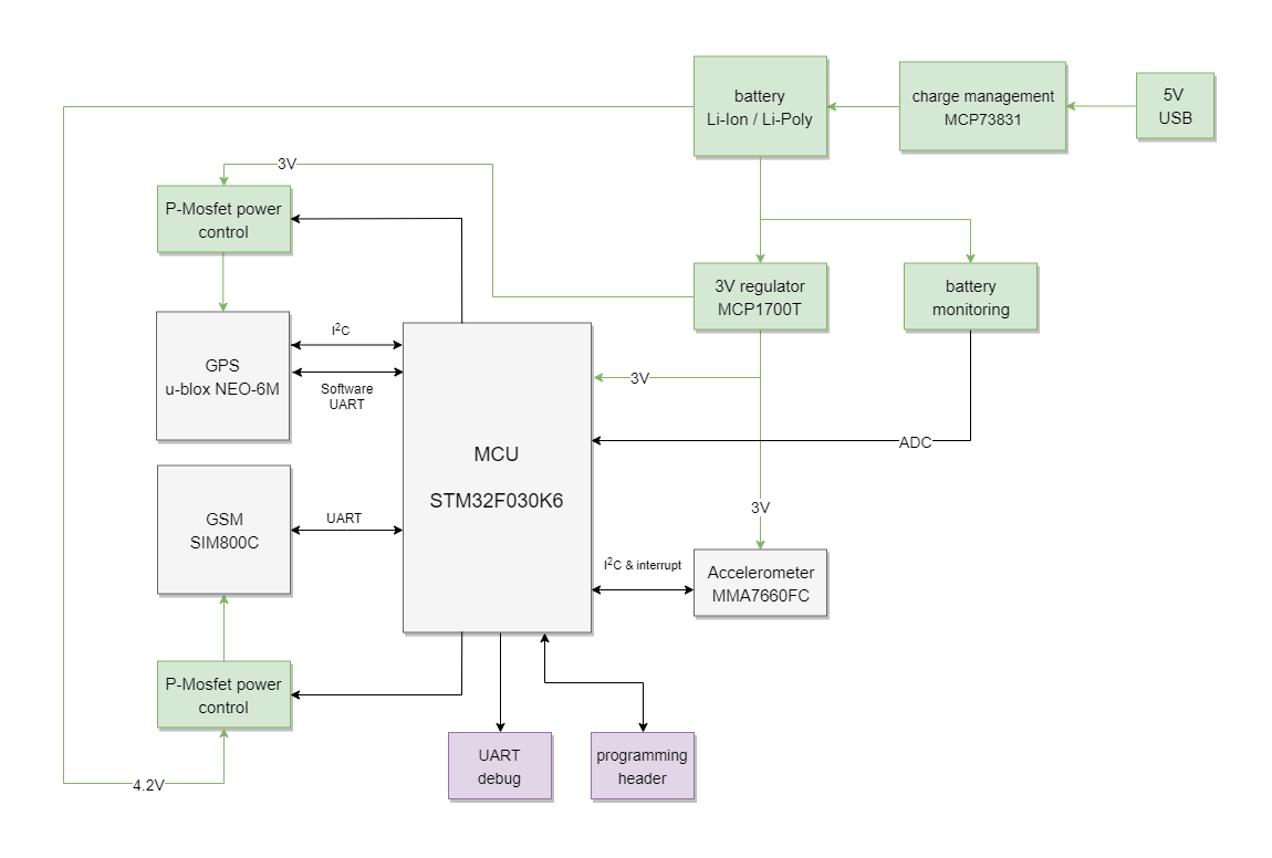
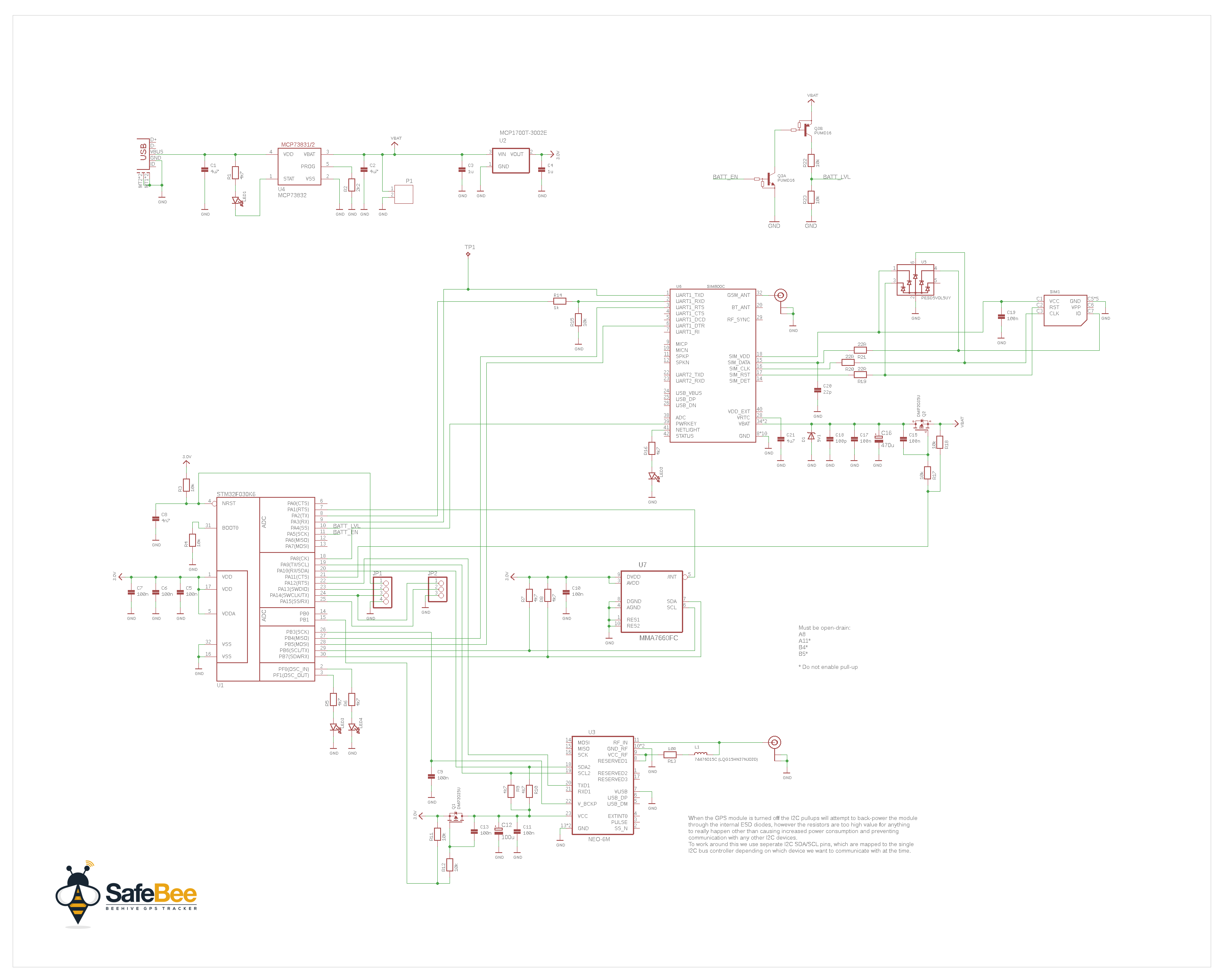
Block Diagram
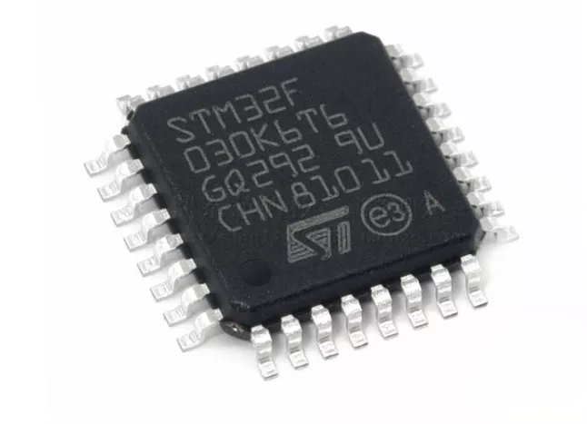
MCU
STM32F030K6
The tracker uses an ST STM32F030K6 microcontroller (ARM Cortex-M0, 32-bit RISC core), with 32KB of flash, and 4KB of RAM, and operates at up to 48MHz. The STM32F030K6 microcontroller operates in the -40 to +85 °C temperature range from a 2.4 to 3.6V power supply. A comprehensive set of power-saving modes allows the design of low-power applications. Currently, the firmware is taking roughly 24KB of flash (with debugging output enabled) and 1.7KB of RAM. The microcontroller is running at 8MHz and is supplied with 3V.
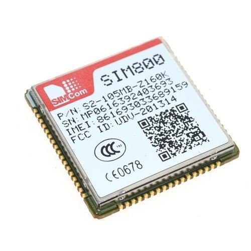
GSM module
SIMCom SIM800C
The GSM module is a SIMCom SIM800C and uses the UART bus to communicate with the MCU. The GSM module is power-gated with a P-MOSFET, controlled by the MCU, as its own low-power modes are not sufficient for this project. SIM800C supports Quad-band 850/900/1800/1900MHz, it can transmit Voice, SMS and data information with low power consumption. With a tiny size of 17.6*15.7*2.3mm, it can smoothly fit into our small board. The module is controlled via AT commands and has a supply voltage range 3.4 ~ 4.4V.
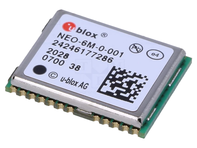
GPS module
u-blox NEO-6M
The GPS module is a u-blox NEO-6M and uses the I2C bus to communicate with the MCU. There is also a UART connection to the microcontroller as a fallback if the I2C interface does not work (usually the case with Chinese fakes). So, the tracker will work with the original NEO-6M as well as Chinese fake modules. The microcontroller implements the UART interface in software (via timer interrupts), operating at 9600 baud. The GPS module is power-gated with a P-MOSFET, controlled by the MCU, as its own low-power modes are not sufficient. The NEO-6M is powered in the range of 2.7 – 3.6V and has a size of 12.2 x 16 x 2.4mm. More details and design considerations can be found in the Hardware Integration Manual of NEO-6 GPS Modules Series and u-blox 6Receiver Description.
Supported GPS modules:
U-blox NEO-5M
U-blox NEO-6M
U-blox NEO-7M
U-blox NEO-M8N
Various Chinese fakes using AT6558 and similar (if the PCB footprint is the same then it will probably work)
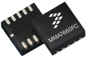
Accelerometer
MMA7660FC
The accelerometer IC is the MMA7660FC and uses the I2C bus to communicate with the MCU. The MMA7660FC is a ±1.5g 3-Axis Accelerometer with Digital Output (I2C). It is a very low power, low profile capacitive MEMS sensor featuring a low pass filter, compensation for 0g offset and gain errors, and conversion to 6-bit digital values at a user-configurable sample per second. In OFF Mode it consumes 0.4 μA, in Standby Mode: 2 μA, in Active mode 47 μA and is powered in the range 2.4 V – 3.6 V. The accelerometer is always active, set up to create an interrupt whenever a shake or orientation change is detected, and is configured with a sampling rate of 8Hz (higher sampling rates improve detection, but also increase power consumption). The interrupt will wake up the microcontroller, where it will run through the main loop. In this loop it checks the interrupt status, and if set it will clear the interrupt and increment a counter at a maximum of once per second. The counter is reset every minute. If the counter reaches 3 the tracker is activated.
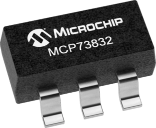
Battery Charger
MCP73832
The Li-Ion battery charging IC is MCP73832, which has a user-programmable charge current and the battery charge rate is set to 450mA. It includes an integrated pass transistor, integrated current sensing, and reverse discharge protection. It is usually recommended to charge Lithium batteries at no more than 0.5C, so the recommended minimum battery capacity to use with the tracker is 900mAh.
With a 2500mAh battery, standby current of 70uA, and waking up every 12 hours for 5 minutes with an estimated average current of 15mA the battery life should be approximately 1.5 years. A poor GSM signal can reduce battery life.
Status LEDs
LED
Description
States
LED1
Battery charging state
OFF: Battery not charging (no USB power or battery fully charged) ON: Charging
LED2
GSM state
OFF: GSM is powered off FAST BLINK: GSM is not connected to a network (usually no signal or no SIM) SLOW BLINK: GSM is connected to the network
LED3
MCU Operating mode
OFF: Standby mode ON: Ready or tracking mode
LED4
GPS state
OFF: GPS is powered off FAST BLINK: GPS is acquiring a lock SLOW BLINK: GPS has a lock
SMS Commands
Command
Description
BEE+STATUS
Returns battery voltage - temperature - GSM signal strength - tracking enabled - is tracking - last GPS coordinates -sensitivity level.
BEE+CLEAR
If the tracker has been triggered this will clear it and stop tracking until the next trigger.
BEE+TRIGGER
Manually trigger tracking (will trigger even if disabled with BEE+DISABLE). Tracking will stay enabled until BEE+CLEAR is received.
BEE+ENABLE
Enable tracking triggers
BEE+DISABLE
Disable tracking triggers.
BEE+NUMBER=0123499988
This sets the mobile number to send tracking - low battery warning and monthly status SMSs to. Other command replies are sent to the number that the command was sent from.
BEE+NUMBER=+441234999888
International numbers must start with + then the country code.
BEE+SENSE=1/2/3
This is the sensitivity level - 1 high sensitivity - 2 medium sensitivity - 3 low sensitivity.
LOW BATTERY: (battery voltage)mV (threshold voltage mV)
LOW BATTERY: 3400mV (3650mV)
Programming
The device firmware can be programmed via the SWD interface, which is the 4-pin programming header on the PCB marked RST (reset), SWD (SWDIO), SWC (SWCLK) and GND (ground). An ST-LINK/V2 USB adapter is needed to program the device, which is available from ebay, aliexpress, and other places for less than £3.
3D Render
3D Render of the board on KeyShot 11 Pro
Debugging
Debugging data is sent out of the UART interface through the TX pin of the debugging header on the PCB, at 115200 baud. This pin is also shared with the SWD interface (SWC). The RX pin is unused but made available for possible use in the future.
Format
(<time>)(<module>)<message>
“time” is in milliseconds and only increments while the microcontroller is not in standby mode. “module” is either “DBG” (general messages), “TRK” (tracker), “GSM”, “GPS”, “SMS”, “MGR” (MGR is the SMS manager which controls when queued SMSs are sent, retried etc.)
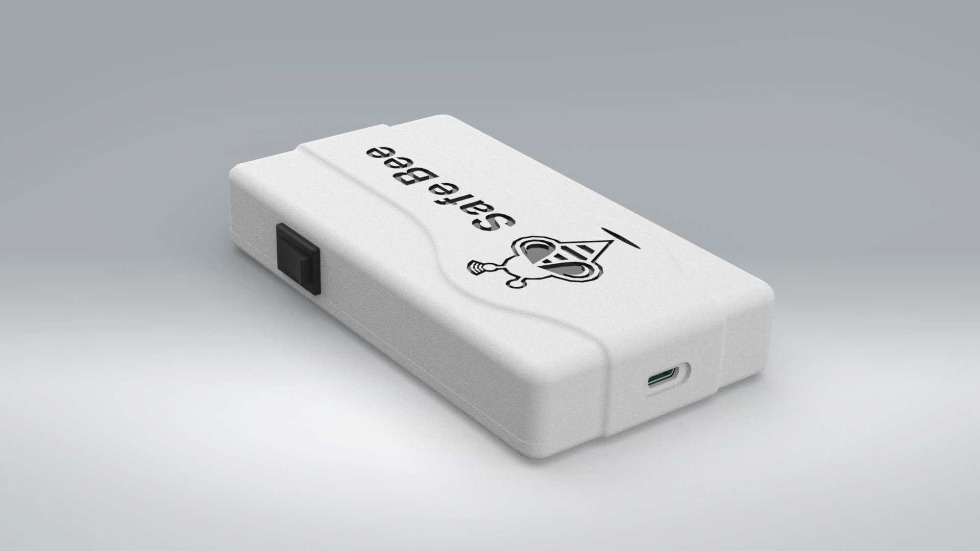
A 3D model of the enclosure is designed using Solidworks with overall dimensions of 60 x 20 x 112 mm. The enclosure has two holes, one for the charging micro USB connector and one to fit a mini rocker power switch. The provided design files (download .STEP and .STL files below) can be used to print your own enclosure in your desired color and material. The screws used to secure the enclosure are M3 x 10mm countersunk screws. Design is made by professional engineer janangachandima and you can find his services on the Fiverr page.
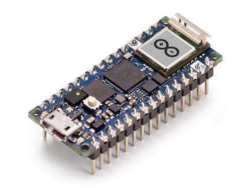
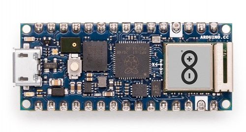
One of the most widely used development boards in the maker community is the Arduino manufactured boards. However, following the release of the $4 Raspberry Pi Pico that came with the onboard in-house silicon tape out RP2040 chip, sparking excitement in the designer world. Continuing the growth of RP2040-based development boards, we saw Adafruit QT Py RP2040 and many more. Today, after four months of introduction, we have Arduino release the Arduino Nano RP2040 Connect to the market at just $24.50 without taxes.
This might sound crazy to have Raspberry Pi manufacturer SOC on an Arduino development board, but this is what makes it unique yet powerful. Giving a quick recap on the integrated SOC RP2040 is a dual-core Arm Cortex M0+ processor running at 133 MHz clock frequency. Justifying the cost of the development board, the manufacturer has provided a u-blox NINA-W102 radio module that allows you to take advantage of Arduino Cloud compatibility. The module gets two Harvard Architecture Xtensa LX6 CPUs operating at a maximum 240 MHz internal clock frequency.
As always Arduino doesn’t stop to surprise us with the number of capabilities provided onboard at a very low cost. The board gets a built-in mic for AI voice recognition and a six-axis smart IMU that detects motion by adding fall sensing and double-tap activation. Adding more of the hardware, we have RGB LEDs and multi-function GPIO pins.
It was an easy choice for Arduino to put an RP2040 at the core of a new board. We felt so strongly about the excellence of this new chip that we knew it deserved a powerful, premium Nano board that is unrivalled in terms of features.
As stated previously, the hardware can be connected to the Arduino Cloud, which makes it much more powerful than all other mini development boards in the market. If you plan to get a development board that can be accessed remotely even after deploying it into projects, you can now do it with the Arduino Cloud access. If the hardware is connected to Wi-Fi, it can do everything as if it was connected through USB. To add more to this, you can also control the Arduino Nano RP2040 Connect through the Arduino IoT Remote app.
For more details on Arduino Nano RP2040 Connect, please visit the official product page.
Arduino is an open-source electronics platform based on user-friendly hardware and software. Arduino boards are popular among beginners in electronics as well as professionals who use them for easy prototyping. For making an Arduino-based project, all that is needed to be done is interfacing the peripherals, code your commands and you are ready to go. Arduino boards can read analog and digital inputs like temperature data, the light intensity on a light sensor, finger on a button, IR detection, etc. and they can turn it into an output like turning on an LED, starting motor, display on LCD, etc. Over the years, Arduino has been the brain of thousands of projects, from everyday objects to complex scientific instruments. Some very well-known Arduino-based projects are ArduPilot (drone software and hardware), ArduSat (a CubeSat based on Arduino hardware and software), Arduinome (a MIDI controller device), and many others.
About Arduboy
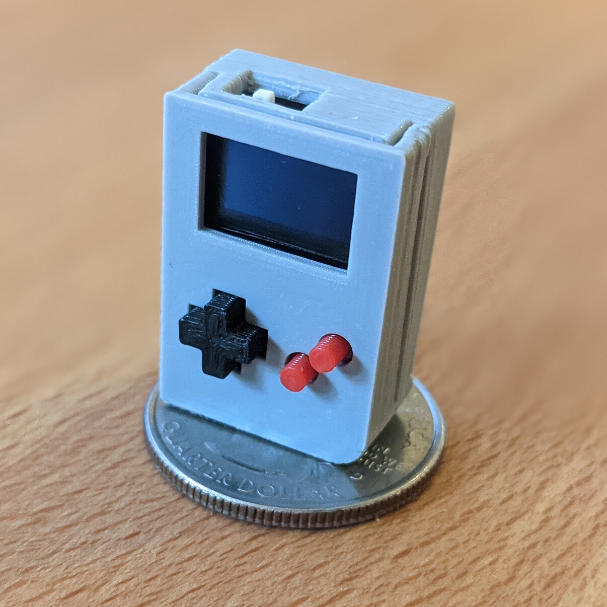
Among all of the Arduino projects, Arduboy is one of the most popular devices. It is a handheld game console based on the Arduino environment. The original version of the Arduboy was 1.6mm thick, with the height and width of a credit card, and was initially designed by Kevin Bates as an electronic business card. Later the touch-sensitive buttons were replaced by physical buttons and included a plastic case for protection. This also raised the thickness of the gamepad. The current version of Arduboy comes with over 200 pre-installed games and can be reprogrammed. Additionally, it is open-source which means you can also create your games and play in them.
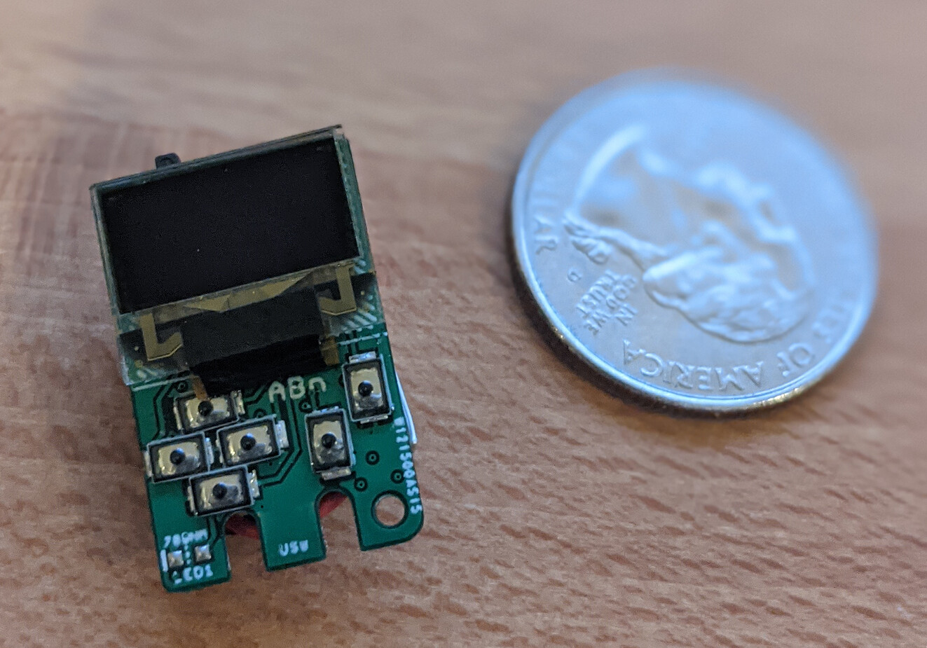
A far more compact version of the Arduboy console is Arduboy Nano which is smaller than an inch tall. It is 26mm tall and features a 0.49″ OLED display with 64×32 pixels. The console is built around the same microcontroller that the original Arduboy used which is ATmega23u4. It is a low-power 8-bit AVR microcontroller. It is also featured in Arduino Pro Micro. The OLED unlike the original Arduboy uses the i2c protocol and fewer pixels. The 0.49 inch OLED display consumes very little power as no backlight is required. As this OLED display makes its light on its own, it has high contrast and wide viewing angle despite consuming less amount of power. All of the pinouts remain the same as the original one and all of the existing games are code compatible. In a nutshell, it has all the features of the original Arduboy but it has just shrunk.
It also has a small 15mm piezo speaker which is very quiet and all of this is powered by a 25mAh Li-Po battery. The game consumes somewhat less than 25mA and so the battery lasts around 1 hour.
The case consists of 3 pieces of sliding enclosure which are 3D printed. The buttons were also painstakingly printed at 2mm/s to retain their delicate shape while printing.
Kevin said this regarding the design inspiration:
“This design is entirely based on something that Ben Rose made and showed me at Maker Faire 5 years ago. I’ve been waiting for them to do something with it, but I couldn’t hold back any longer! The people must know!”. He also added, “Currently there are no plans to produce this but if it goes bananas online, I’ll consider finding someone to help me turn this into a real product. Keychain anyone?”
AVR microcontrollers are RISC architecture-based microcontroller series that have on-chip flash memory for data storage. The popularity of ARM microcontrollers can be seen by the range of applications it has. They are used in home automation, touch screen, automobiles, medical devices, and defense. They are also quite popular among hobbyists and makers. Most AVR microcontrollers use the In-System Programming (ISP) feature. ISP is a feature of microcontrollers that allows uploading of a program while the chip is on the system. This aids the end-users as they can program the hardware device according to their needs. Three pins are dedicated for the programming which are Serial Clock (SCK), Master-In-Slave-Out (MISO), and Master-Out-Slave-In (MOSI). All types of memory on the micro-controller can be accessed using the SCK, MISO, and MOSI pins while holding the RESET pin LOW.
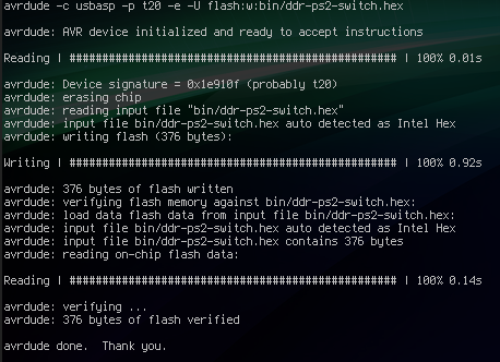
USBASP is an open-source ISP (In-System Programming) programmer for AVR devices. If someone wants to develop programs that use the UART of Atmega32, you need to upload code using ISP. USBASP can be used for programming other AVR micro-controllers also. It can be used for burning the boot loader. The LED on the board indicates power. It goes off while uploading code, giving an additional indication. Newer AVRs use much faster programming techniques like TPI and UPDI. But someone may want to flash newer TPI-based AVR microcontrollers with an old USBASP board. Kevin Cuzner documented how to program TPI-only AVR microcontrollers using a USBASP device.
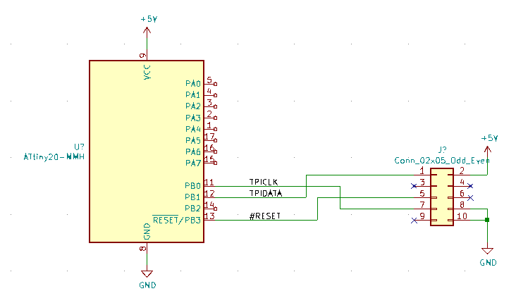
TPI Programming: A summary
Before going into the steps involved in the programming process, let’s first get an overview of TPI programming. The Tiny Programming Interface (TPI) is the only programming interface available in some newer AVR microcontrollers. TPI interface method consists of two layers Physical layer and the Access layer. The physical layer consists of two operations: transmit and receive. The TPI Access layer controls the mode of operation. TPI interface method needs only 3 pins for usage which are Reset, TPIDATA, and TPICLK. TPIDATA is a bidirectional data line unlike in the SPI method, where 2 data lines are used for transmission and reception of data.
Steps to program TPI based AVR MCUs using USBASP programmer
Kevin listed the following steps that are involved in programming TPI-only AVR MCUs using USBASP:
Buy another USBASP programmer as one of them will be the programmer and another one would be the target that is going to become TPI capable.
Switch the programming jumper on the target by shorting the appropriate header (sometimes labeled JP1, sometimes labeled JP2). It’s a two-pin jumper and is NOT the target voltage jumper, nor the “slow clock” jumper.
Connect the programmer USB to the PC. Don’t connect the target to the PC.
Connect the two USBASPs using the 10-pin ISP ribbon cable.
Use avrdude to program the downloaded firmware (be sure to choose the correct hex file for the ATmega used on the target programmer).
For interfacing, connect the TPIDATA pin of the TPI header to the MOSI pin of MCU, TPICLK to ISP CLK, and RESET to the corresponding RESET pin. Further, it is necessary to ensure that the AVR is running at 5V.
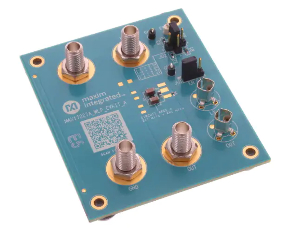
Maxim’s MAX17227A is a 400 mV to 5.5 V input, 2 A nanoPower boost converter with short-circuit protection and True Shutdown™
Maxim’s MAX17227A is a nanoPower boost converter, capable of delivering a load up to 2 A peak inductor current and providing True Shutdown, cycle-by-cycle inductor current limit, short-circuit, and thermal protection. During shutdown, current drawn from the input pin is 1 nA. The MAX17227A offers ultra-low quiescent current, small total solution size, and high efficiency throughout the load and line range. These features make it ideal for battery-powered applications where extended battery life is required and high efficiency is necessary at all power levels.
MPS’ 50 V, 5 A and 6 A, three-phase power stage drivers offer PWM and enable inputs
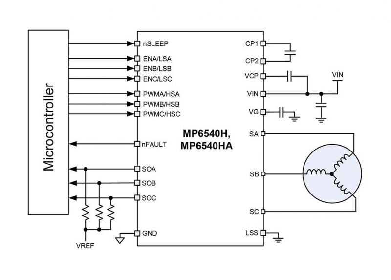
The MP6540H and MP6540HA from Monolithic Power Systems are three-phase brushless DC motor drivers. These devices integrate three half-bridges consisting of six N-channel power MOSFETs, pre-drivers, gate drive power supplies, and current-sense amplifiers. The MP6540H has enable (EN) and PWM inputs for each half-bridge, while the MP6540HA has separate high-side (HS) and low-side (LS) inputs, otherwise they are identical. The MP6540H can deliver up to 6 A of peak current and 5 A of continuous output current, based on thermal and PCB conditions. The MP6540H uses an internal charge pump to generate the gate drive supply voltage for the high-side MOSFETs, and a trickle charge circuit that maintains sufficient gate drive voltage to operate at 100% duty cycle. Internal safety features include thermal shutdown, undervoltage lockout (UVLO), and overcurrent protection (OCP). The device is available in a QFN-26 (5 mm x 5 mm) package.
Features:
5.5 V to 50 V operating supply voltage
Three integrated half-bridge drivers
Maximum 5 A output current, 6 A peak current
MOSFET ON resistance: HS + LS 45 mΩ
MP6540H: PWM and EN inputs; MP6540HA: HS and LS inputs
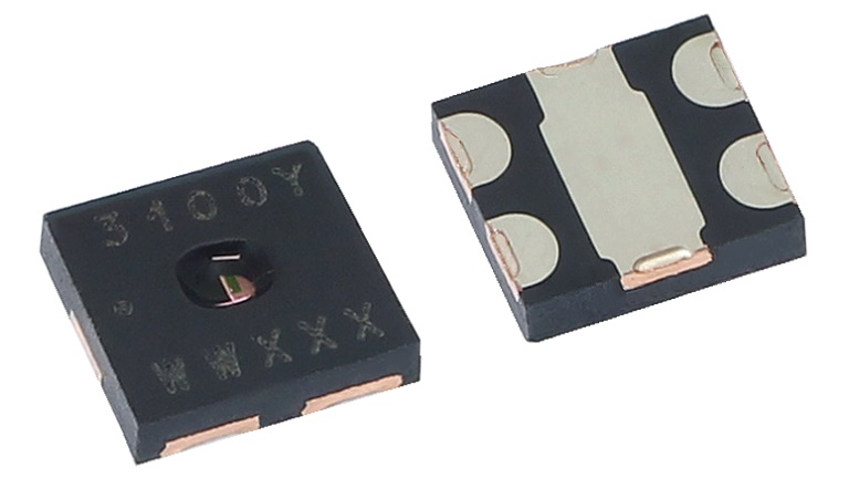
The Vishay Semiconductors’ VEML6031X00 high accuracy ambient light sensor supports an easy-to-use I2C bus communication interface
The Vishay Semiconductors’ VEML6031X00 high accuracy ambient light sensor supports an easy-to-use I2C bus communication interface and additional interrupt feature. The ambient light result is available as digital value. The VEML6031X00 is ideal for automotive applications, including display backlight controls, infotainment systems, rearview mirror dimming, interior lighting control systems, and head-up displays.
Key features
High accuracy ambient light sensor supports an easy-to-use I2C bus communication interface
16-bit resolution sensor in a small opaque 2.67 mm x 2.45 mm package
Incorporates a high sensitive photodiode, a low noise amplifier and a 16-bit A/D converter
Surface-mount package type
Additional features
Ambient light sensor (ALS) integrated modules
2.5 V to 3.6 V supply voltage range (VDD)
Communication via I2C interface
Multiple I2C Slave address options available:
VEML6031X00: 7-bit I2C Slave address 0x29
VEML60311X00: 7-bit I2C Slave address 0x10
1.7 V to 3.6 V I2C bus H-level range
Floor life of 4 weeks, MSL 2a, according to J-STD-020
World Telecommunication and Information Society Day (WTISD) takes place on May 17th every year, to connect the world and promote digital technologies. This year, the theme is to Accelerate Digital Transformation in challenging times. As time goes by, people started to realize the inconvenience of conservative manufacturing as well as the urgency of digital transformation, especially after the COVID-19 crisis. Thus, both governments and the private industrial sectors have turned to IIoT as a better solution for smart manufacturing in this changing time.
How Can IIoT Help?
IIoT (Industrial Internet of Things) offers innovative ways to boost operational efficiency and introduce a new wave of industrial services. IIoT, also known as Industry 4.0, brings together Connectivity, Data & Computational Power, Analytics & Intelligence, and Human-Machine Interaction. It is the network of a variety of industrial devices connected by telecommunication technologies, enabling the systems to monitor, collect, exchange, analyze as well as deliver data.
Connectivity, Data & Computational Power
Connectivity is the foundation of Industry 4.0 and part of the foundational technologies applied along the value chain. This is achievable with the help of the high capacity, high speed, low latency and reliable 5G network. 5G ensures the delivery of IIoT technologies and helps keep all machines and robots perfectly in sync in real-time.
Analytics & Intelligence
IIoT achieves incredible levels of efficiency, productivity, and performance by integrating machine-to-machine communication with industrial data analytics. For example, industrial AI inside a refinery pipe can detect corrosion to provide real-time production data, allowing a factory to reveal extra capacity. Another example of IIoT intelligence is digital twin. It allows computers to “tell” operators how to maximize productivity or predict a malfunction before it happens, potentially saving billions of costs.
Human-Machine Interaction
To transform form traditional, labor-intensive manufacturing processes to modern, autonomous ones, the adoption of smart manufacturing fits in the future roadmaps of hyperautomation. For instance, AGV (Automated Guided Vehicle) is indispensable for smart warehousing and smart factories, fully utilizing space and labor resources. When human operates at the ordering systems, AGVs will receive signals and carry required items to the picking workstations. HD video of the factory floor from a camera attached to an AGV can also be streamed with the help of 5G. AGV helps to realizes human-machine interaction and is the best choice for manufacturers to save energy, reduce costs, and increase productivities.
Fibocom Wireless Solutions
IIoT requires stable wireless communication network coverage and fast inter-AP roaming switching to ensure efficiency and stability in various industrial scenarios. Fibocom has been an active player in the sector of IIoT, helping to accelerate digital transformation around the world. Fibocom provides one-stop IoT (Internet of Things) services including wireless communication modules and IoT application solutions. Whether it is to improve production efficiency or to reduce management costs, Fibocom is capable for offering 5G connectivity with faster transmission speed, better carrying capacity, and lower network latency, demonstrating the huge application potential of 5G in IIoT.
Fibocom’s 5G wireless communication modules are designed to offer eMBB (enhanced Mobile Broadband), URLLC (Ultra Reliable and Low Latency Communications), as well as mMTC (massive Machine Type Communications). Supporting 5G standalone network (SA) and non-standalone (NSA) network architectures, Fibocom 5G wireless module series supports the Sub-6GHz and mmwave bands, and is compatible with 5G NR, LTE and WCDMA standards. It eliminates customers’ investment concerns at the initial stage of 5G construction, responding to the commercial demand for rapid landing. Meanwhile, Fibocom 5G modules come with a rich set of interfaces including USB3.1 (3.0), USB2.0, PCIe3.0 (2.0), SPI, SDIO, GPIO, UART, etc. It has been certified by various regional operators, industry associations and local regulation, satisfying different deployment requirements for customers worldwide.
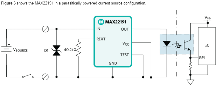
App note from Maxim Integrated on their parasitically powered digital input interface chip which is used favorably on industrial applications. [via]
A digital input (DI) is a circuit designed to receive a binary signal transmitted from an industrial sensor and translate that input into a reliable logic signal for a programmable logic controller (PLC) or industrial controller. Common examples of industrial binary signals are pushbuttons and/or temperature or proximity threshold indicators. The MAX22191 parasitically powered DI circuit can monitor Type 1 and Type 3 sink and source binary input signals for PLC and industrial circuits.
Industrial digital inputs with the MAX22191 – [Link]