ZED-F9R High-Precision Sensor Fusion GNSS Solution

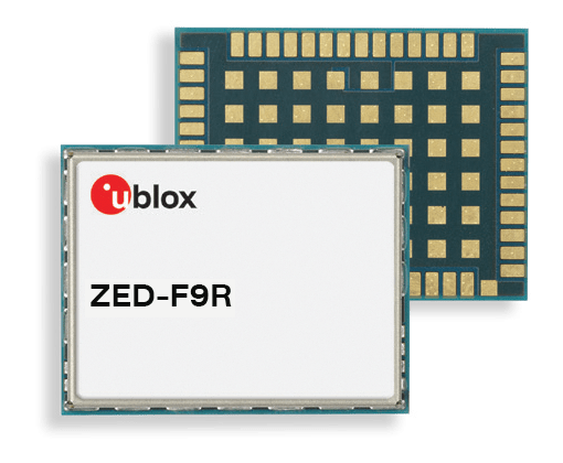
u-blox’s F9R dual-band GNSS module is a fully integrated solution for fast time-to-market

u-blox’s ZED-F9R positioning module features the u-blox F9 receiver platform providing a reliable multi-band GNSS sensor fusion solution for industrial applications in a compact form factor. The wide bandwidth allows receiving of many satellite signals in parallel, resulting in the high availability of RTK solutions and quick convergence time. The module operates under an open sky, in the wooded countryside, in difficult multipath environments, and even in covered areas. Designed for autonomous industrial applications like agricultural machinery or heavy trucks, the ZED-F9R is the ultimate solution for applications where control and position availability are critical.

The ZED-F9R module has an integrated inertial measurement unit (IMU) for RTK positioning in obstructed environments. The sophisticated built-in algorithms fuse the IMU data, GNSS measurements, wheel ticks, correction data, and a vehicle dynamics model to provide optimal positioning accuracy where GNSS alone would fail.

The device is a turnkey self-contained solution, which provides the best possible performance: no latencies or similar system considerations to worry about. This eliminates the technical risk and effort of selecting and integrating RF components and third-party libraries such as precise positioning engines.

The C102-F9R application board with a field-configurable CAN converter allows efficient evaluation of ZED-F9R without porting host libraries.

Features

  • Centimeter-level accuracy in the most challenging conditions
  • Continuous navigation when GNSS is obstructed
  • Multi-band, multi-constellation enables fast convergence: BeiDou, Galileo, GLONASS, GPS
  • Easy integration of RTK for fast time-to-market
  • Wide bandwidth receives L1/L2/L5 signals simultaneously for improved RTK performance
  • Turnkey solution includes dead reckoning, RTK, and position engine

more information: https://www.u-blox.com/en/product/zed-f9r-module

BQ25171-Q1 – 800-mA linear battery charger for 1- to 2-cell Li-ion, LiFePO4, and 1- to 6-cell NiMH

Texas Instruments bq25171-Q1 Linear Battery Charger is an automotive rated 800mA linear charger for 1-cell and 2-cell Li-Ion, Li-Polymer, and LiFePO4, in addition to 1-cell up to 6-cell NiMH battery applications. The device has a single power output that charges the battery. The system load can be placed in parallel with the battery as long as the average system load does not prevent the battery from charging fully within the safety timer duration. When the system load is placed in parallel with the battery, the charge current is shared between the system and the battery.

The Texas Instruments bq25171-Q1 has three phases for charging a Li-Ion battery: precharge to recover a fully discharged battery, fast-charge constant current to supply the bulk of the charge, and voltage regulation to reach full capacity. The device charges a NiMH in constant current mode only and terminates the charge cycle when the programmable timer expires or the battery voltage exceeds the VOUT_OVP threshold. In all charge phases, an internal control loop monitors the IC junction temperature and reduces the charge current if an internal temperature threshold, TREG, is exceeded.

Block Diagram

Features

  • AEC-Q100 qualified for automotive applications
    • –40°C ≤ TA ≤ 125°C temperature grade 1
    • HBM ESD classification level 2
    • CDM ESD classification level C4B
  • 40V load-dump tolerant to support charging back-up battery directly from the main battery, 3V to 18V operating
  • Automatic Sleep Mode for low power consumption
    • 350nA battery leakage current
    • 2µA input leakage current when charging disabled
  • Support multi-chemistry battery
    • 1- to 2-cell Li-Ion, Li-Poly, and LiFePO4
    • 1- to 6-cell NiMH with intermittent-charging support
  • External resistor programmable operation
    • VSET to set battery regulation voltage from 3.5V to 8.4V for Li-Ion, or 1- to 6-cell for NiMH
    • ISET to set charge current from 10mA to 800mA
    • CHM_TMR to set battery chemistry as Li+ or NiMH, and charge timer duration
  • High accuracy
    • ±0.5% charge voltage accuracy
    • ±10% charge current accuracy
  • Charging features
    • Precharge current 20% of ISET
    • Termination current 10% of ISET
    • NTC thermistor input to monitor battery temperature
    • CE pin for charging function control
    • Two Open-drain output for status and fault indication
  • Integrated fault protection
    • 18V IN overvoltage protection
    • VSET based OUT overvoltage protection
    • 1000mA overcurrent protection
    • 125°C thermal regulation; 150°C thermal shutdown protection
    • OUT short-circuit protection
    • VSET, ISET, CHM_TMR pins short/open protection

more information: https://www.ti.com/product/BQ25171-Q1

DR8072A embedded router board offers dual 2.5 GbE, WiFi 6 connectivity

Known best for router boards like the DR6018-V3, Suzhou-based embedded wireless solutions manufacturer, Wallys Communication, recently added a new router board; the DR8072A, to their impressive list of wireless solutions.

Wallys has in recent times been developing a growing number of router boards based on several Qualcomm SOCs and this latest board is no different. Designed based on the Qualcomm AP-HK09 reference design, the board features Qualcomm’s recent IPQ8072A SOC, a member of the Qualcomm networking Pro 1200 family which delivers more 802.11b/g/n/ax bandwidth and offers a faster clock rate (2.2HGZ) than is obtainable in earlier Qualcomm IPQ6000 series SOCs like the IPQ6010 used in the DR-6018-S router released not too long ago.

Most of the standout features of  DR8072A  can be attributed to the IPQ8072A SOC and the willingness of the Wallys team to break them out to users. Also referred to as the hawkeye, the SOC supports 4×4 dual-band concurrent operation for up to 8x spatial 802.11b/g/n/ax streams (4×4 MU-MIMO 5GHz and 4×4 MU-MIMO 2.4GHz) and also features TX Beamforming with around 17dBm per chain.

The IPQ8072A is responsible for the incredible data speed obtainable 0n the DR8072A, facilitating 1147 Mbps data transfer rates at 2.4GHz and up to 2475 Mbps at 5GHz. This according to Wallys, enables the DR8072A to provide:

“mobile access to high-bandwidth video streaming, voice, and data transmission for office and challenging RF environment in factories, warehouses establishment,”.

Designed for use in rugged applications, the DR8072A supports operating temperatures as extreme as -20ºC to +70ºC and a working humidity range of -5% to +95% (non-condensing), making it the perfect solution for most industrial and outdoor applications.

Some highlight features and specifications of the DR8072A include:

  • Qualcomm Atheros Quad Core ARM Cortex 64-bit A53 Processor IPQ8072A
  • 1x 512MB, DDR4 2400MHz 16-bit interface
  • 2.412~2.472GHz / 5.150~5.825GHz
  • Support 11ax TX Beamforming
  • Support 11ac/ax MU-MIMO DL and UL
  • Support OFDMA DL and UL.  OFDMA: BPSK, QPSK, 16-QAM, 64-QAM, 256-QAM, 1024-QAM
  • Supports Dynamic Frequency Selection (DFS)
  • Tri-band support with 5G SBS
  • On-board 4×4 2.4GHz MU-MIMO OFDMA 802.11b/g/n/ax, max 17dBm per chain
  • On-board 4×4 5GHz MU-MIMO OFDMA 802.11a/n/ac/ax, max 17dBm per chain
  • 1x MiniPCIe Slot with PCIe 3.0
  • NOR Flash: 8 MB
  • NAND Flash: 256MB
  • 8x U.FL Connectors
  • 1x S/W Reset Button
  • 1x DC Jack Connector: 12V
  • 4x 1Gbps Ethernet Port,
  • 2x 2.5Gbps Ethernet Port
  • 2x USB 3.0 Port
  • 1x JTAG 20 Pin Connector
  • 1x Serial Port 4 Pin Connector
  • Operating: -20ºC to 70ºC,
  • Storage: -40ºC to 90ºC

No price information is currently available for the DR8072A  but the project page on Wally’s website shows availability.

More information on features, specifications, availability of the …. can be obtained from the product’s page on Wally’s Website.

USB UPDI Programmer PCB for AVR Micrcontrollers

AVR is a microcontroller family developed in 1996 by Atmel, now acquired by Microchip Technology since 2016. AVR generally refers to the 8-bit RISC architecture line of ATMEL AVR microcontrollers. They are very popular in embedded systems. They are very common in maker and hobbyist embedded applications and they are also included in Arduino boards. AVR is based on the modified Harvard architecture in which the program and data are stored in separate physical memories. They allow reading data items by special commands. In AVR architecture, Flash memory, EEPROM, and SRAM are all integrated on a single chip. This eliminates the need for external memory.

AVR Programming Methods

In-system programming uses the SPI (Serial Peripheral Interface) which is a full-duplex master-slave-based interfacing technique. The synchronization is done by the rising or falling edge of the clock applied. The disadvantages of the SPI interface are that the speed depends on the target clock and four pins are utilized in the interface. SPI is a very simple type of programming interface. Then comes JTAG which was introduced in 40 pin AVRs. In JTAG, the speed is faster and does not depend on the target clock. But it also needs four port pins for usage.

The TPI Interface was introduced in low-end microcontrollers like some selective microcontrollers in the ATtiny family. It is a 2-wire interface that uses reset as clock and another dedicated data pin. PDI interface is very similar to the TPI interface. It is fast and can cope up with a baud rate of 230,400. UPDI interface is the latest interface by Microchip technologies. It is used in almost all new AVR microcontrollers like tinyAVR, megaAVR, and AVR-Dx. This programming interface is a cross between Debug-Wire and PDI but, it only uses a single line like Debug-wire. However, it is a serial interface without a clock so, the speed is not as fast as PDI.

UPDI Programmer PCB

Stefan Wagner from Germany designed a simple programmer which can program new AVR microcontrollers. The USB-to-serial chip used here is CH330N. It comes in an easy SOIC-8 package and only needs few components to work. In addition, it works fine with both 3.3V and 5V. UPDI interface only needs 3 pins: VCC, GND, and UPDI. First of all, USB to serial conversion is done by the CH330N IC. Then the serial pins RX and TX are tied together with a 4k7 resistor or any suitable resistor and that node is connected to the UPDI pin of the AVR device. The schematic of the board is as follows.

Source: https://github.com/wagiminator/AVR-Programmer/blob/master/PyUPDI_Programmer/PyUPDI_Programmer_schematic.pdf

The programmer works with pyupdi and Arduino IDE. pyupdi is a Python utility for programming AVR devices with the UPDI interface using a standard TTL serial port. This allows makers and designers to program AVR microcontrollers from their favorite environments and languages like Arduino IDE which uses C/C++ or Raspberry Pi environment which uses Python.

The complete project including the Gerber file can be found here: https://github.com/wagiminator/AVR-Programmer/tree/master/PyUPDI_Programmer

Quicklogic QuickFeather Alexa Close-Talk Reference design

While voice/speech-controlled embedded devices and systems are more popular thanks to the success of devices like the Amazon Alexa, their design is still quite a hassle due to the complexity of the engineering and algorithms involved. Since Alexa Skills became a thing, and Amazon opened up device APIs and SDKs that allow the integration of Alexa into devices, the hassle on the software side has reduced, but the hardware challenge still existed as there were no plug-and-play, easy-to-use, optimized audio modules in the market.

All of these reasons put together was why fabless semiconductor manufacturer, Quicklogic, developed the EOS S3 ultra-low-power multicore MCU which featured best-in-class audio front-end and powers Quicklogic’s Quickfeather platform, which was developed to make building voice-based embedded solutions easier.

Based on (and compatible with) Adafruit’s open-source Feather Board, the Quickfeather was designed to enable the next generation of low-power Machine Learning (ML) capable IoT devices, and this combined with the QuickLogic’s Open Reconfigurable Computing (QORC) Initiative, and the EOS™ S3 Voice Processor, could be used to create superior user experience and long battery life voice-based system.

To shorten time to market for designers using the platform and make leveraging the potentials in these combinations easier, Quicklogics recently released the QuickFeather Alexa Close-Talk Reference design; created for Voice-Initiated, Hands-Free, Alexa Built-In Devices with Close-Talk Support.

According to Quicklogics,

“This is the first available always-listening, Close-Talk qualified smart hearable reference design based on QuickLogic’s ultra-low-power Arm® Cortex®- M4 Microcontroller”

and it can be used by designers and manufacturers to “evaluate the “Alexa” Built-In Close-Talk experience, optimized for battery-powered products” and build Proofs-of-Concept.

The EOS S3 integrates Sensory’s Low Power Sound Detection (LPSD) technology and runs DSP Concepts’ TalkTo noise suppression and beamforming technology that helps create an intuitive voice-based system, but beyond the reference design also shows how can integrate motion, and other Artificial Intelligence (AI) and Machine Learning (ML) use cases based SensiML’s AI Software Platform that already supports QuickLogic’s QuickFeather development kit.

Some highlight features of the Reference Design include:

  • Alexa Wake Word Engine (WWE) running in the EOS S3 voice processor
  • Hardware-optimized Low Power Sound Detection (LPSD) technology from Sensory™
  • Support for one or two microphone use cases with DSP Concepts’ TalkTo noise suppression and beam forming technology
  • Connectivity to Alexa Voice Service via Wi-Fi
  • Built on top of 100% open-source hardware QuickFeather dev kit and QORC open-source software tools
  • Comes with a QuickLogic QuickFeather Development Kit including the EOS S3 Low Power Voice Processor – Supported by 100% Open Source Hardware Development Kit and Software Tools
  • Espressif ESP32-WROVER-E WiFi Development Kit for WiFi connectivity
  • Adafruit I2S Audio Decoder for supporting playback from Alexa Voice Service directly to a standalone speaker
  • QuickLogic microphone daughtercard that supports variable microphone spacing
  • QuickLogic sturdy PCB cradle to reliably connect all components together

The reference design board is available for sale on the Quicklogics website for $149.

More information on the features of the board and its purchase, along with a manual showing how to use it can be found on the products page on Quicklogic’s Website.

RP2040 M.2 Card with M.2 Connectivity Form Factor

RP2040 M.2 card

There has been a lot of discussion about the Raspberry Pi’s RP2040 SoC in the past few months after the release of the Raspberry Pi Pico. The RP2040 SoC is also popular for its high-frequency clock covering a large range of applications at a very low cost. Timonsku a hardware designer has come up with a design for the M.2 interfacing of the SoC. This allows the miniaturization of the hardware at low power requirements. The edge connector of the design has a size of M.2 B key.

Timonsku’s design is an RP2040 M.2 card consisting of an RP2040 SoC, a WS2812 intelligent control LED, and a Qwiic connector. WS2812, an intelligent control LED light source in which the control circuit and RGB chip are combined in a package of 5050 components. It is a “simple, scalable and affordable full-color LED”. The board also comes with external GPIO pins allowing the input for the program from outside the CPU or providing the output to the user. The board also has reset and boot buttons on it.

Twitter Thread of RP2040 M.2 Card

Additionally, M.2 form factor is popular in SSDs. It is also called the Next Generation Form Factor (NGFF) due to its internal mounting capacity. This allows compatibility with the computer expansion cards and similar connectors. It is a good alternative to the mSATA standard, which uses the “PCI Express Mini Card physical card layout and connectors”.

There has been a discussion on the interfacing of the board with Desktops or Laptops as they come with M.2 slots. However, according to Timonsku, the M.2 slot of the RP2040 M.2 card may not be used with USB signals. As the M.2 specification does not compulsorily require them. Also, it would be difficult to automate the board while it is present on the laptop or computer. Hence, GPIO-level access would be necessary to work on the boot and reset signals.

Piunora Carrier Board

The Twitter thread of Timonsku shows the compatibility of the RP2040 M.2 card with the Piunora carrier board. This carrier board is also compatible with the popular Raspberry Pi CM 4 and transits it to Arduino R3 like form factor. Piunora carrier board has completed its goal of funding on the Crowd Supply at this point time.

The RP2040 M.2 card is still in the design phase and it is probable that the design would be soon open-source. For more information and updates on the card, you can keep checking Timonsku’s Twitter thread.

via Hackster

Electromagnetic near-field PCB Probes are open source

In modern compact electronic circuits, there are several components on a confined PCB area, and so, the electromagnetic effects induced from one component may affect the surrounding components. This disturbance is known as Electromagnetic Interference (EMI). The source of the radiation must be identified in PCBs to predict the EMC of electronic circuits. Electromagnetic compatibility (EMC) is the ability of electrical equipment and systems to function acceptably in their electromagnetic environment, by limiting the unintentional generation, propagation, and reception of electromagnetic energy which may cause unwanted effects such as EMI. Near-field scanning is the general method for identifying radiation sources in PCBs.

Electromagnetic near-field scanning

Near-field scanning is used for estimating localized electromagnetic emissions. The far-field is a region in which the field acts as normal electromagnetic radiation. But in the near-field region, electric and magnetic fields can exist independently. Additionally, in the near-field region, one type of field can dominate the other. E-field and H-field probes are used for electromagnetic near-field scanning. E-field probe measures point-to-point the electric field strengths locally. On the other hand, the H-field probe measures the magnetic field strengths locally.

E-field and H-field probes: An overview

The E-field probe consists of a short dipole antenna, a detector diode, a non-perturbing transmission line, and a readout device. Three orthogonal dipoles are generally used in an E -field probe to provide a response that is nearly isotropic for all polarizations of the incident field. Optical fibers, together with a suitably modulated light source, may be used to form a wide-band non-perturbing data link from the dipole and detector to a remote readout [1].

The H-field probe consists of a printed circuit magnetic loop and a transmission line. The magnetic flux from the loop will induce a high-frequency waveform that travels through a transmission line to the receiver. The transmission line is mostly a microstrip line.

Source: https://charleslabs.fr/en/project-Electromagnetic+interference+mapping

Implementing near field E-field and H-field probes on a printed circuit board is difficult mainly because it involves designing and implementation of non-perturbing transmission lines.

The below shown near-field probes are designed by Ketan Desai. He is a student of Electrical Engineering at the University of British Columbia.

The complete project including Gerber files can be found at: https://github.com/ketszim97/NearField_PCB_Probes#readme

Reference:

[1] H. Bassen and G. Smith, “Electric field probes–A review,” in IEEE Transactions on Antennas and Propagation, vol. 31, no. 5, pp. 710-718, September 1983, doi: 10.1109/TAP.1983.1143126.

JLCPCB & EasyEDA Finally Show UP Together

Design & Order on EasyEDA to Get $10 Voucher!

The Cheapest PCB prototype supplier and the first FREE online EDA tool show up together actually is not a piece of “new” news for many fans of JLCPCB or EasyEDA, but today i would like to give a brief introduction to those friends who did not know us. JLCPCB & EasyEDA,these two companies which sounds irrelevant while belong to the same group named JLC group.

Only $2, you can get 5 pcs PCB boards in JLCPCB

Make the PCB prototype much Easier and Cheaper.

JLCPCB is reputed as one of the most popular and powerful PCB Suppliers in china. Situated at the silicon of China, Shenzhen, JLCPCB has been in the PCB manufacturing and assembly industry for over 15 years, with assembly technologies of the highest quality standards, fastest delivery turnaround (as fast as 24hours), lowest manufacturer direct prices, and support via dedicated customer service. JLCPCB provide Free online price calculator,which make the PCB price automatically and transparently showed. And the Gerber Viewer give all the details of PCB design, helps much customers avoid the potential fault during manufacture.

EasyEDA, An Easier& Powerful Online PCB Design Tool

Make the Free EDA Tool into Reality

EasyEDA as a free, zero-install, Web and cloud-based EDA tool suite that integrates powerful schematic capture, hybrid mode circuit emulation, and PCB layout in a seamless cross-platform browser environment for electronics engineers, educators, students, and hobbyists.

As a totally free online EDA tool, EasyEDA has more than one million real-time updated components created on its parts library and users can create or import their own common libraries. And Benefit from China’s leading electronic components distributor – LCSC ,

EasyEDA supports direct links to more than 200,000 real-time, in-stock components at LCSC .

Designers can refer to stocks, prices, and order at any time during design.

The Combination of JLCPCB &EasyEDA

Makes the PCB &SMT Manufacture Easier

As far as we know,PCB prototype is an essential part of the development of any electronics product ,while the efficient EDA tool ensures reliable design.So the joint of JLCPCB the qualify PCB supplier and EasyEDA make the whole process from design to manufacture much more efficient than ever before.

From EasyEDA to JLCPCB, there is no need to generate the Gerber file into the manufacture system in JLCPCB. There is an interface where you can get your design directly manufactured through this button. There are few tips for how to place PCB or SMT orders directly from EasyEDA.

1 When you get PCB Design in EasyEDA; Use parts in JLCPCB Assembled library to design PCB, make better decisions with real-time visibility into parts availability and pricing. Confirm parts selection with confidence.

2 One click to order at JLCPCB;Once finishing your PCB design, click “Generate PCB Fabrication File(Gerber)” to preview your board, then order your design at JLCPCB with one click, and the Gerber files will be automatically uploaded on JLCPCB. Get $10 Voucher Now!

3 Simply generate the BOM and Pick&place files from EasyEDA, and upload them directly into our platform. Our system is compatible with EasyEDA formats.

4 Parts Confirmation; Since you’ve used parts from JLCPCB library, our system identifies all parts your need directly from the BOM and all parts can be confirmed automatically.

5 Quote & Order;Review the parts placement and check the component orientation, to know how we will assemble your board and see the instant price for SMT assembly service.

6 Order Delivering; Track the production process in real-time, and receive professionally assembled PCBs in One Week.

The Joint Activity of JLCPCB&EasyEDA is in Process

Get $10 off for your PCB +SMT Order Now!

New EDC Series Supercapacitors Offer Capacitance Values from 0.047 to 1.5 Farad

High Power Density, Coin Cell Supercapacitors from Cornell Dubilier in Stock at TTI

TTI, Inc., a leading specialty distributor of electronic components, has stock for immediate shipment of multiple values of the Type EDC series Stacked Coin Cell Package Supercapacitors from Cornell Dubilier (CDE).

The EDC series offers capacitance values from 0.047 to 1.5 Farad with voltages from 5.5VDC up to 6.3VDC. Supercapacitors can replace or extend battery life in onboard memory backup. With quick-response and recharge times, these supercapacitors offer higher power than batteries and greater energy than typical aluminum electrolytic capacitors without degradation over millions of charge-discharge cycles.

Three different case configurations are available including horizontal, vertical and radial-lead PCB mounting. The operating temperature for the EDC series is -25°C to +70°C. Applications include real-time clock (RTC) backup, power failure backup and battery assist.

To learn more, visit CDE Type EDC Coin Cell Supercapacitors at TTI.

MicroMod STM32 Processor improves MicroMod applications

SparkFun’s processor board improves MicroMod applications with its Arm® Cortex®-M4 32-bit RISC core

The SparkFun MicroMod STM32 processor board improves MicroMod applications with its Arm Cortex-M4 32-bit RISC core. This little processor board provides an economical and easy-to-use development platform for situations that require more power with minimal working space. With the M.2 MicroMod connector, connecting the STM32 processor is a breeze. Simply match up the key on the processor’s beveled edge connector to the key on the M.2 connector and secure it with a screw (included with all carrier boards). The STM32 is one of the most powerful and economical microcontrollers available, so to be able to add it to MicroMod carrier boards is a huge advantage for any project.

The STM32F405 processor is based on the high-performance Arm Cortex-M4 32-bit RISC core and can operate at a frequency of up to 168 MHz. This core features a floating point unit (FPU) single precision that supports all Arm single-precision data-processing instructions and data types. It also implements a full set of DSP instructions and a memory protection unit (MPU), which enhances application security. This processor board utilizes the DFU bootloader for uploading code and incorporates an extensive range of enhanced I/Os and peripherals. To complement the STM32F405 processor, SparkFun has also added an additional 128 Mb (16 MB) serial Flash memory chip to the underside of the board.

Features

  • Arm 32-bit Cortex-M4 CPU with FPU
    • Adaptive real-time accelerator (ART Accelerator™) allowing 0-wait state execution from Flash memory
    • Frequency up to 168 MHz
    • Memory protection unit
    • 210 DMIPS / 1.25 DMIPS/MHz (Dhrystone 2.1)
    • DSP instructions
  • 1 Mbyte of Flash memory
  • 192 Kbytes of SRAM including 64 Kbytes of core coupled memory (CCM) data RAM
  • Flexible static memory controller supporting compact Flash, SRAM, PSRAM, NOR, and NAND memories
  • Clock, reset, and supply management
    • 1.8 V to 3.6 V application supply and I/Os
    • 32 kHz oscillator for RTC with calibration
    • Internal 32 kHz RC with calibration
  • Low-power operation
    • Sleep, stop, and standby modes
    • VBAT supply for RTC, 20×32 bit backup registers + optional 4 KB backup SRAM
  • Debug mode
    • Serial wire debug (SWD) and JTAG interfaces
    • Cortex-M4 Embedded Trace Macrocell™
  • Advanced connectivity
    • USB 2.0 full-speed device/host/OTG controller with on-chip PHY
    • USB 2.0 high-speed/full-speed device/host/OTG controller with dedicated DMA, on-chip full-speed PHY and ULPI
    • 10/100 Ethernet MAC with dedicated DMA: supports IEEE 1588v2 hardware, MII/RMII

more information: https://www.sparkfun.com/products/17713

TOP PCB Companies