Hamish Morley has designed a microcontroller module to help enthusiasts and developers accelerate their ideas faster into products — a versatile Arduino-compatible board in a really small package, called Minima.
“Minima is a small and versatile Arduino compatible programmable microcontroller module in a surface mount format. It is an ideal stepping stone between traditional jumper-based prototyping and producing your own custom PCB’s,” says Hamish.
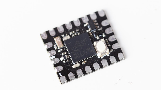
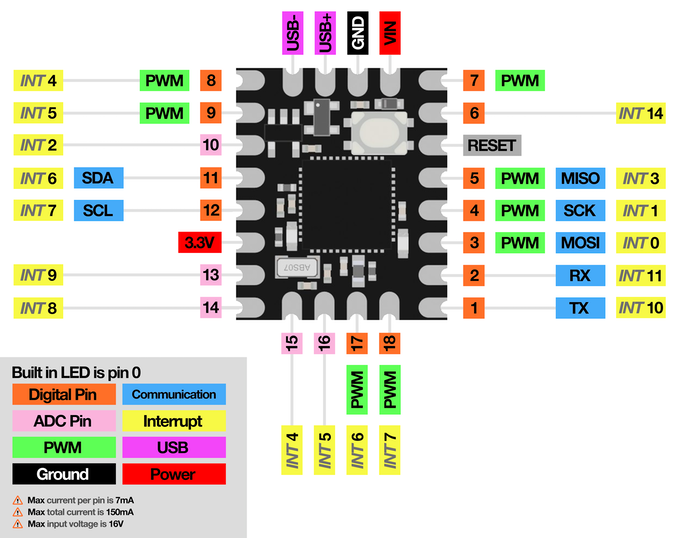
Minima is one of the smallest Arduino-compatible boards with features that offer a great user experience. The board features a 32-bit Microchip SAMD21G18A processor, the same as the one on popular boards like Arduino Zero, MKR Zero and Adafruit Feather. Minima also features a 3.3V 150mA voltage regulator that is efficient, readily available, and ideal for edge IoT applications – it can be powered from a max of 16V. There’s also a diode in the board that helps to protect your components from damage and sudden smoke.
The board is really really small in size like I said earlier, but it has all the necessary functionalities that it is expected to have. So it is a perfect solution for a wide range of projects like wearables, motion tracking and IoT.
Features and Specifications include:
It has a very small size (19.8mm x 16.6mm)
It is easy to solder (no need for intricate soldering or reflowing)
It enables rapid prototyping (no need to bother about the time you’d use to solder tiny components, just base your design around the Minima footprint and accelerate your prototyping and designing)
CPU: 32-bit Microchip SAMD21G18A processor with a clock-speed of 48MHz
256KB of flash storage
32KB of RAM
Very low power consumption
3.3V, 150mA Voltage Regulator (converts the input voltage down to the working voltage of your components)
ESD suppressor for native USB (helps to improve reliability for mission-critical applications)
2x LEDs: 1x Green RX/TX LED for the Native USB, and 1x Red user programmable LED
Offers reverse voltage protection (provides protection for all of the components in case you accidentally connect1 the VIN/GND reversed)
18x GPIO (5x pins are analog-capable)
SPI, I²C, and UART interfaces
PWM and hardware interrupts
SMD-ready (hand soldering or reflow)
1x Reset button
Dimensions: 19.8mm x 16.6mm
Minima has been already launched on Kickstarter and already surpassed it’s $ 1,387 funding goal by almost $1,000. Manufacturing is expected to start in May while shipping will be done in July and August.
By the way, the developer has reassured that everything about the board is going to be open source, with all files available for download on GitHub soon.
“Keeping in line with the open source ethos of the Arduino community, I am uploading all of the hardware/software files onto GitHub so you can make your own board if you want,” he said.
Further details on the board including schematics and rewards are also available on the Kickstarter page where the board is launched.
If you have ever loved the idea of recharging batteries with solar power or have been looking for a great way to minimize the use of traditional batteries, then you might want to take a closer look at the new Solarcell that has just launched and funded on Kickstarter by a team of developers.
“Solarcell is a new generation of Lithium rechargeable batteries with USB-C connection, containing high power capacity while maintaining a high level of safety,” the team writes. “We offer a wide range of battery models to help you power up any kind of devices you have and use frequently.”
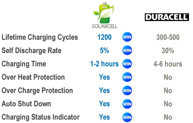
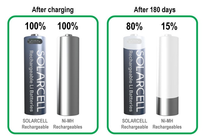
Solarcell has some benefits over regular disposable batteries. It was designed to help you save some costs. Solarcell is powered by Lithium polymer (Li-Po) rechargeable batteries whose life cycle is about 10 years (1200 charge cycles). So imagine how many disposable batteries that you’d have used in those years (about 1200 disposable batteries). Li-Po batteries also store and generate higher energy than other technologies, so Solarcell should offer much higher energy capacity and higher voltage output.
Solarcell was also built with convenience in mind.
“With our USB-C connection, you can charge Solarcell with any USB-A to C and USB-C to C cable. Hence, you can choose to charge them from your wall socket, power bank, laptop or even with a solar panel. All these options can further enhance your convenience and make sure all your batteries can always be charged up easily.”
Features:
All types of battery models for all devices
Has a high energy density
Has multiple ways of charging
Provides renewable energy and quite environmentally friendly
Has a fast recharge time
Has a low self-discharge rate
Guarantees maximum safety
Has a LED indicator (turns red when the Solarcell is being charged through the USB-C cable and green when it’s done charging)
Important protection features including power leakage protection, short circuit protection, high-pressure protection and over-current protection
Solarcell batteries can be quickly charged in about 1-2 hours and the batteries have lower self-discharge rates and longer storage life, so there is the ease of usage and convenience. There’s also a custom-designed PCB in the battery that helps to ensure safety.
What’s more? You can be sure that you are not going to be polluting your environment because Solarcell is environmentally friendly.
The project has been launched already on Kickstarter and already surpassed it’s HK$ 20,000 (~$2,600 US) funding goal. Rewards start at USD36 for the early bird AAA combo with 4x AAA Solarcell rechargeable battery, USD40 for the early bird AA combo with 4x AA Solarcell rechargeable battery and USD60 for the early bird 18650 combo with 2x 18650 Solarcell rechargeable battery. All options include a USB A to 2 USB Type-C cable.
You may want to check the Kickstarter page where the project was launched for other important details on the project. Shipping is due to start in May this year.
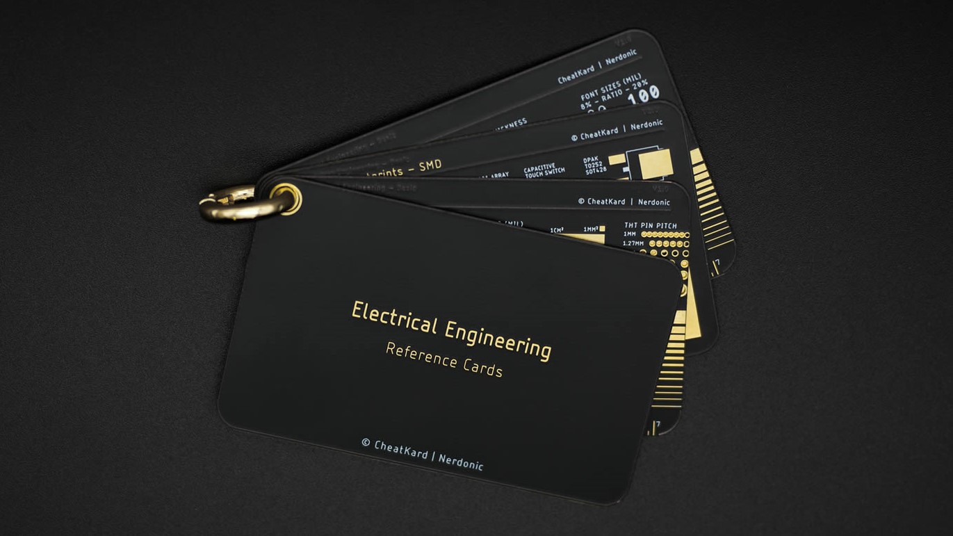
Are you an electrical engineer and always looking for reference sheets to assist you with calculations and assumptions? Then this credit card-sized CheatKard will help you to ease your life as an electrical engineer. Nerdonic, known for its custom electronics, IoT & rapid prototyping, had introduced the Nerdonic PCB business reference card. This reference card was nothing but a business card provided to the businesses and customers, which was not made up of paper. With positive feedback from the community, the company launched a Kickstarter crowdfunding project to help electrical engineers with small-sized reference cards for all kinds of work (related to electrical engineering).
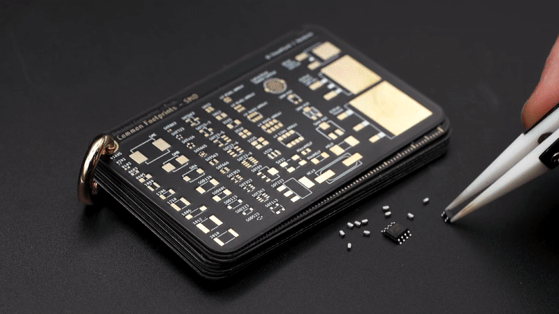
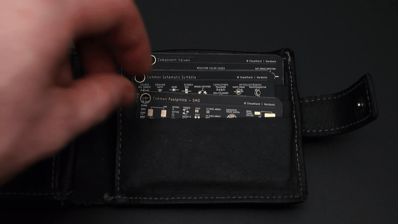
It has become difficult for all professionals to get books and read hundreds of pages or Google to get some information. To make this easy, Nerdonic’s credit card-sized CheatKard is portable, allowing you to boost your efficiency in all circumstances. Even if you do not have access to the internet, you can always refer to this portable reference card. This product is made in a credit card size because you can keep it in your wallet, being accessible anywhere and anytime.
“Gone are the days of trawling through an abundance of varied search results and forum posts to find the answer you need or flipping to page 102 in your chunky Electrical Engineering textbook,” Nerdonic says. “CheatKards are small, lightweight, with concise, accurate information and references for you to use whenever you need them.”
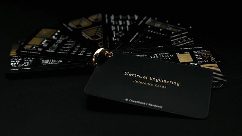
The aesthetics of the reference cards add value to the overall usefulness. CheatKard comes in gold plated letters with a black background, giving it a luxurious look. The product’s front side has gold-plated lettering and a key-ring hole, while the backside is blank for you to write your details. The vital part of the CheatKard is the cards within these two that include the most resourceful and easily accessible information for all the levels (related to electrical engineering), let that be a student or a professional.
Coming to the information that you will get with this CheatKard is as follows:
PCB Design Card: VIA size gauge/Size (MM & MIL)/Amps across copper thicknesses, Copper thickness conversion, PCB layer makeup for 1/2/4 layer PCB, ENIG & Tin plating finishes, Panelization (Mouse-bites/V-cut), PCB thermals explanation, Meanders explanation, PCB finishes, Ruler (INCH), and many more.
Laws And Theory Card: OHMs law, Resistors in series, Resistors in parallel, Capacitors in series, Capacitors in parallel, Kirchhoff’s law (First and Second), Coulomb’s law, Faraday’s law, Lenz law.
These are the details you will get in a single set of CheatKards; isn’t it amazing? For you to go back to the basics of law and circuit theory, you have a reference card or even to get resistor values. More information on the resources available in the reference cards is provided by the manufacturer on the crowdfunding project page.
One of the things I like about the product is the portability, and the amount of information available is excellent. Buying this always gives you the pride of getting a tree planted with the amount paid for this product. Thanks to Nerdonic, who has supported the environmental cause through selling such valuable and resourceful products. As expected, the project is funded 25 times more than the goal. If you are interested in getting the reference cards, the crowdfunding is still live with the base amount of £28 to get the CheatKard.
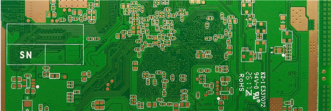
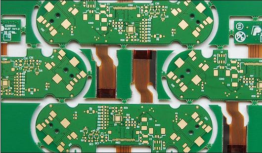
Printed Circuit Boards (PCBs) are popular among engineers, developers, and hobbyists and they are readily available for use in many devices that we use in our daily lives. You can find them in portable electronic devices, industrial machines, heavy equipment, communication devices and consumer electronics. The PCBs we see today are usually very complex and comprised of different shapes and materials. Some are flex and rigid, and have variety of components that are wired together to perform a specific task. PCBgogo is an experienced PCB manufacturer that provides turnkey service for PCB assembly prototype and small-batch PCB fabrication. They offer various types of PCBs, fabrication service, and in this article we will talk about 3 different types.
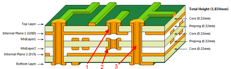
A multilayer PCB is ta PCB that has multiple layers of copper, which is laminated and joined together, and then the components are soldered on top and bottom sides. The inner layers are actually the double sided circuit that are combined with each other to form one thick PCB with multilayers. The components are electrically connected via copper tracks and vias, and pads/ holes link the interconnections. The vias are of different types like PTH, blind and buried. The result is the complex PCB with maximum circuitry on smaller PCB size.
Due to complex processing and evolving technology, demands for PCB layout procedure that can achieve the desired requirements are needed. Also the problems that were occurring in the single or double sided PCBs like noise and stray capacitance was also an issue that caused the invention of multilayer PCB. Multilayer PCBs are usually available from 4 layers to 12 layers, depending on the application and requirements. The layers are usually in even numbers like 4 layer PCB or 8 layer PCB, this is because the odd numbered layers will cause problems of circuit wrapping and similar type issues. The multilayer PCBs are costly to produce compared to single sided because of the extra steps involved during PCB fabrication, however their application are very huge. For example a smartphone can feature a PCB with up-to 8 layers and a military electrical equipment can feature a PCB with up-to 100 layers. This type of PCB with so many layers are very rare and costly.
What are some of the advantages of multilayer PCBs?
Miniature Size: Multilayer PCB is small in size. The size is reduced due to multiple layers being stacked on each other, and connected by “vias”. This enables more compact, dense, solid and smaller sized PCBs. We can find multilayer PCBs being used in mobile phones, laptops, and wearable electronics.
Less weight: Because of its small size, multilayer PCBs are usually light weight and can be easily portable and used in handheld electronics.
High-Quality: Multilayer PCBs offers high quality, because they are fabricated in a very well organized manner, and the amount of effort and work load put into their fabrication is definitely more than that of single or double layer PCBs. Hence more quality and reliability results.
Durability: High pressure is applied to bind the multiple layers with each other. The high temperatures and heat environment through which these PCBs go during fabrication process and bonding agent and protective layers make these PCBs solid, strong and durable.
More Density: Multilayer PCB offers higher density compared to its counterpart single and double sided PCBs. This is because the density of a PCB is directly proportional to the number of components soldered on a per unit size of PCB. For example 20 components placed on per square inch of PCB is denser than the PCB having 15 components per square inch.
More Functionality: Due to its high density, more circuitry is incorporated in lesser PCB space. Therefore, more computing and more powerful and speedy architecture is possible. This is highly demanded in high computation electronics like quantum computing, artificial intelligence, crypto currency mining machines, graphic cards and super computers
Ease of Installation: In many old electronic types of equipment like tvs, we see that the power supply section, video processing section, and display driver sections are all fabricated on separated PCBs, and they are integrated with each other via different connectors and sockets and complex wiring required. However reverse is the case today. Modern LED TV comes in a PCB that has the power supply, LED driver circuit, and mother board all incorporated on a single PCB and a single point of connection is required to install in the enclosure and lesser wiring/harness is required. This helps in ease of installation and dismantling the unit when repairs and troubleshooting is required.
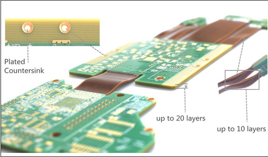
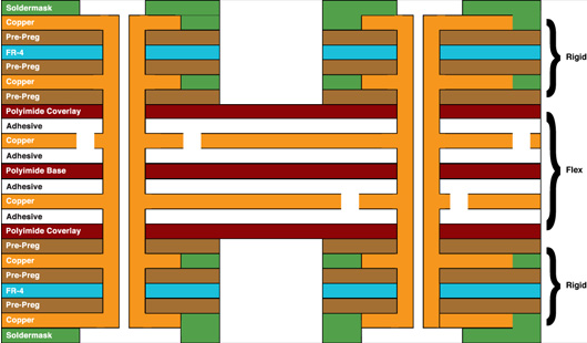
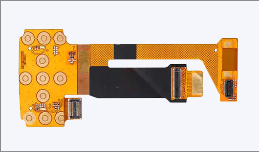
Another PCB service PCBgogo offers is the rigid-flex printed circuit board. What are rigid-flex printed circuit boards? They are the composite boards of rigid boards and flexible boards. When you examine most rigid-flex circuits, you realize that they are multi-layered. However, a rigid-flex PCB can house one or several flex boards and rigid boards, which are then connected through internally/externally plated-through holes.
Rigid-flex PCBs have a thin profile and feature variable shapes. This makes it suitable for ultra-thin and ultra-light packages. Can solve many problems in traditional hardboard technologies. Rigid-flex PCBs make it easier to install more components in a smaller space because they can change the shapes according to specific outlines. This helps reduce the size and weight of the final products and overall system costs. Also, the compact profile of rigid-flex PCB makes it the ideal choice for fine line and high-density circuits in HDI technologies.
Rigid-flex PCBs also offer freedom in packaging geometry. This makes is it suitable for applications in various industries like aerospace, military, medical equipment, and consumer electrics. The rigid-flex PCBs can be customized to any size or shape to fit the housing designs and 3D designs, enabling designers to meet different requirements in specific applications.
Rigid-flex PCBs also offer better mechanical stability due to the stability of rigid boards and the flexibility of flexible boards. This forms a stable structure for the entire package while retaining the reliability of the electrical connection and flexibility needed for installation in small spaces.
Rigid-flex PCBs perform greatly under harsh environments. They have high shock and high vibration resistance so that they can work well in high-stress environments. They also feature fewer cables and connectors, thereby reducing safety risks and maintenance in future use.
Rigid-flex PCBs require fewer interconnectors and related components/parts. It helps to simplify the assembly operations, making the rigid-flex PCBs easier to be assembled and tested. Rigid-flex PCBs are very suitable for PCB Prototypes.
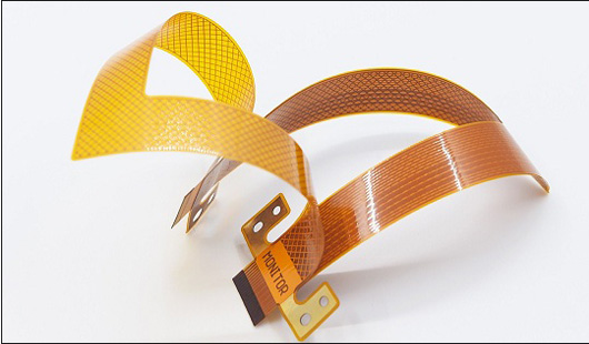
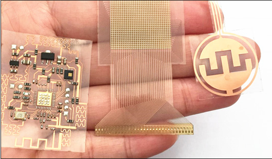
Flexible PCBs (FPC) are PCBs that can be bent or twisted without damaging the circuits. This means the boards can be bent freely to conform to any desired shape during applications. Flexible materials, such as Polyamide, PEEK, or conductive polyester film are used to create these PCBs. When you examine the dielectric layers in FPCs, you see that they are typically homologous sheets of flexible polyimide material. While The dielectric materials in rigid PCBs are usually the composite of epoxy and glass fiber woven cloth. In many PCBs, you can find a layer of solder mask on both sides. The solder mask has gaps, and the SMT pads or PTH holes are exposed to enable components to be assembled. However, in the case of FPC, you find a cover coat instead of a solder mask. The cover coat is a thin polyimide material that can be drilled or laser-cut to access the components.
The manufacturing process of FPCs and rigid PCBs are similar. But FPCs need special tools to hold them in a fixed position because of their flexibility. Regarding price, FPCs are more expensive than rigid PCBs, however, they offer many benefits like improving the cost performance, space-saving, weight-reducing, and high reliability, etc. FPCs offer many benefits. You can find them as connectors in various applications. Due to its excellent flexibility, you can extend the service life of the circuits and save much space. You can find applications of FPCs in smartphones and medical equipment that require many interconnections in a compact package.
Another advantage of FPCs is that they are lightweight and have a smaller volume than rigid PCBs and can be designed to smaller sizes for its flexibility. This makes FPCs ideal to replace bulky circuits in some applications. FPCs offer better resistance and movement performance. They are easy to wrap without breaking and damaging, making them very suitable for outdoor electronics, sports equipment, and wearable electronics.
FPCs have no mechanical connectors during applications. This improves durability in harsh environments. It also enables better heat dissipation than rigid PCBs. This makes it suitable for application in computer components, televisions, printers, and gaming systems.
Even though Flexible PCBs have so many unique advantages in various applications, they still cannot replace rigid PCBs. PCBgogo has a strict quality control system to ensure that the PCBs are manufactured and assembled correctly with high-quality standards.
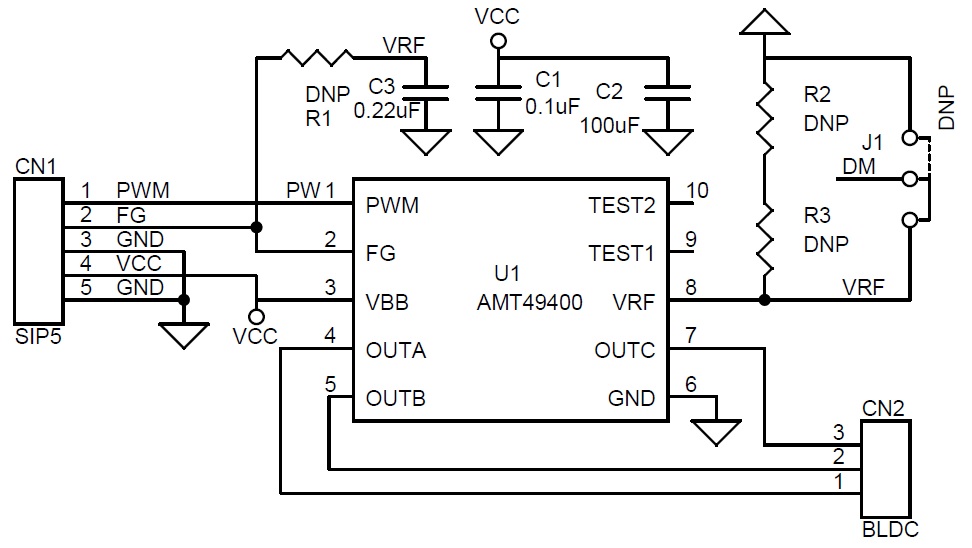
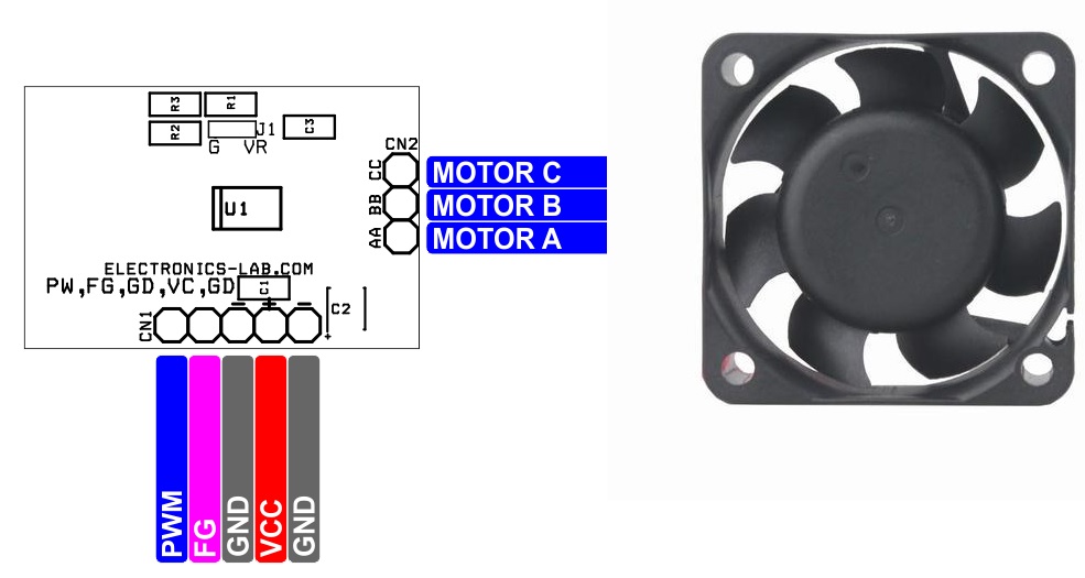
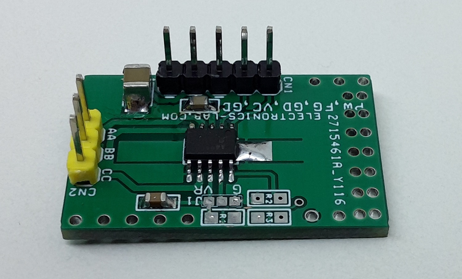
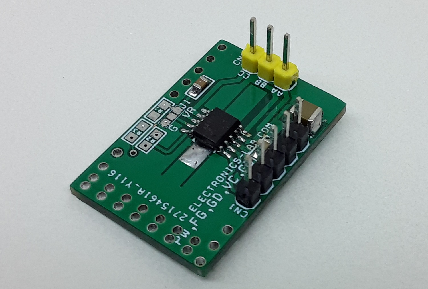
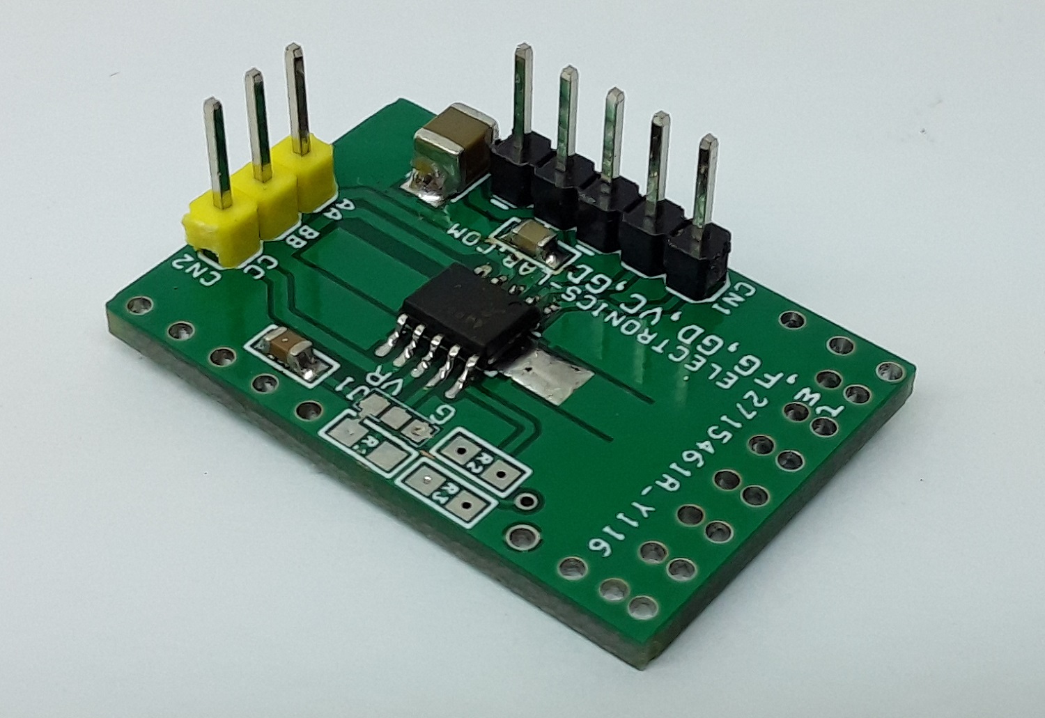
Driving a 3-phase brushless DC motor is very easy with this project. It is a simple and easy-to-build project that requires only a few external components. The circuit is based on AMT49400 IC which is an advanced 3-phase, Sensorless, brushless DC (BLDC) motor driver with integrated power MOSFETs. The chip includes the field-oriented control (FOC) algorithm which is fully integrated to achieve the best efficiency and acoustic noise performance. The motor speed is controlled by applying a duty cycle signal to the PWM input. Users may use Arduino, microcontroller, or discrete circuit to generate PWM for the speed controller. It is a hassle-free easy to use board, just connect the 3 phase brushless motor, connect the power supply and feed PWM to control the speed of the motor. This project is the best choice to drive a FAN motor, small pumps, and brushless toy motors, etc. The circuit also outputs FG speed output information which can be used for feedback. Chip also has a short circuit protection feature that prevents damage to the IC or motor. Any of these three conditions: phase to GND, phase to VBB, and phase to phase will trigger the OCP event, and the AMT49400 will stop supplying current to the motor immediately. The OCP can recover after a power cycle or PWM demand cycle. If the OCP restart mode (EEPROM setting) is “time”, the OCP can recover after 5 seconds.
The integrated field-oriented control (FOC) algorithm achieves the best efficiency and dynamic response and minimizes acoustic noise. Allegro’s proprietary non-reverse start-up algorithm improves start-up performance. The motor will start up towards the target direction after power-up without reverse shaking or vibration. The Soft-On Soft-Off (SOSO) feature gradually increases the current to the motor at “on” command (windmill condition), and gradually reduces the current from the motor at the “off” command, further reducing the acoustic noise and operating the motor smoothly.
Lock Detect: A logic circuit monitors the motor position to determine if the motor is running as expected. If a lock condition is detected, the motor drive will be disabled for 5 seconds before an auto-restart is attempted.
Note 1: We have tested this project in stand-alone mode with PWM input. IC also features a simple I2C interface for setting motor-rated voltage, rated current, rated speed, resistance, and start-up profiles etc. The I2C interface is also used for on/off control, speed control, and speed readback. Refer to the datasheet to configure the chip in I2C mode, The PWM pin is used as SCL in the I2C mode, FG pin is used as SDA in I2C mode.
Note 2: The board has been designed to use A5936 or AMT49400 IC but it is tested with AMT49400 IC, all optional components are provided to use with A5936 3-Phase Sensorless Sinusoidal Fan Driver IC, refer the datasheet to configure this board for A5936 IC.
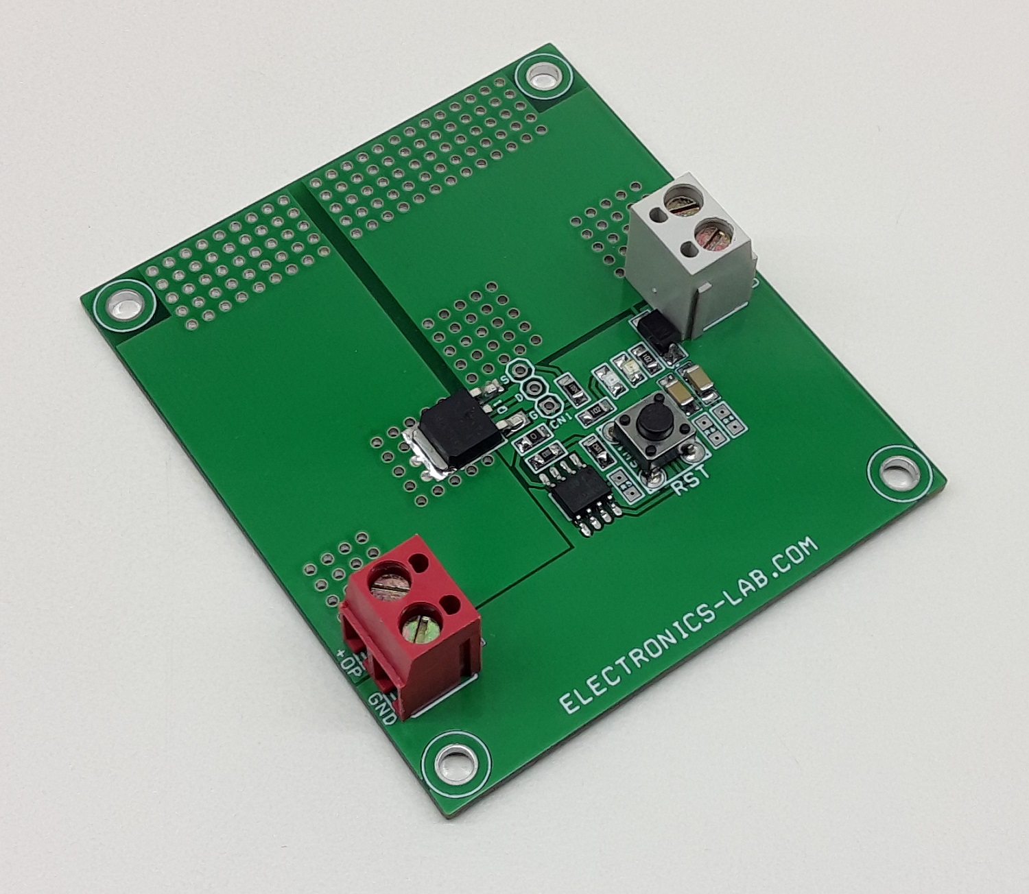
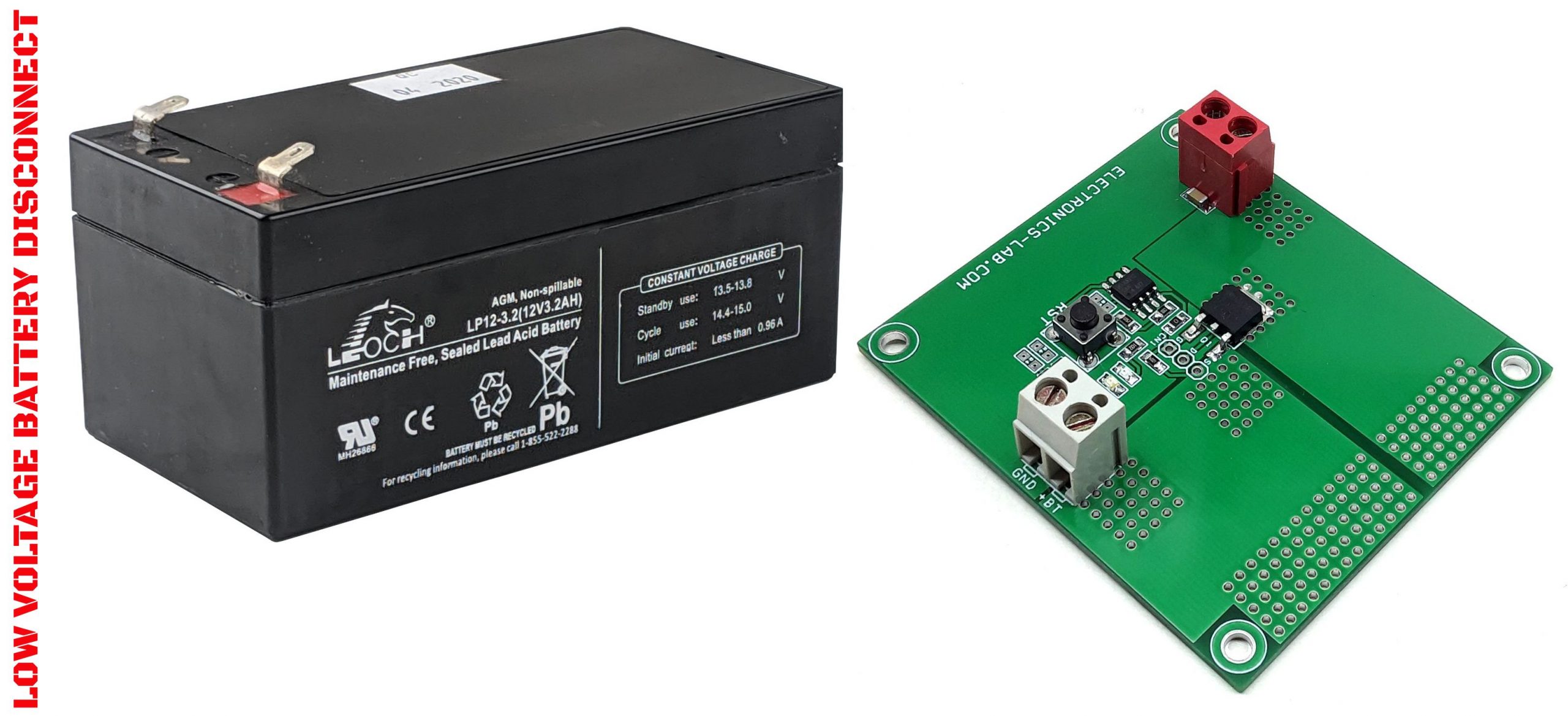
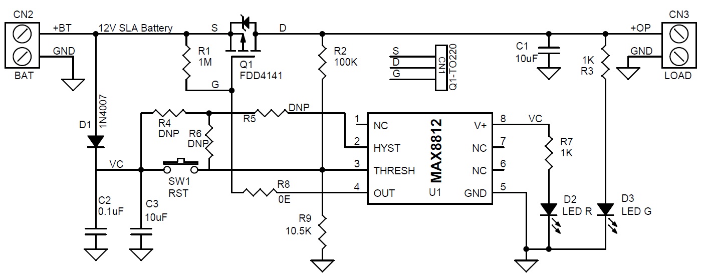
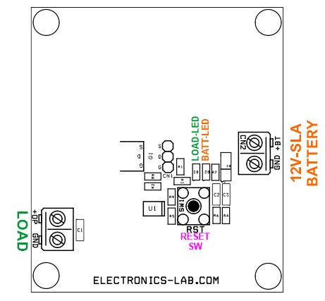
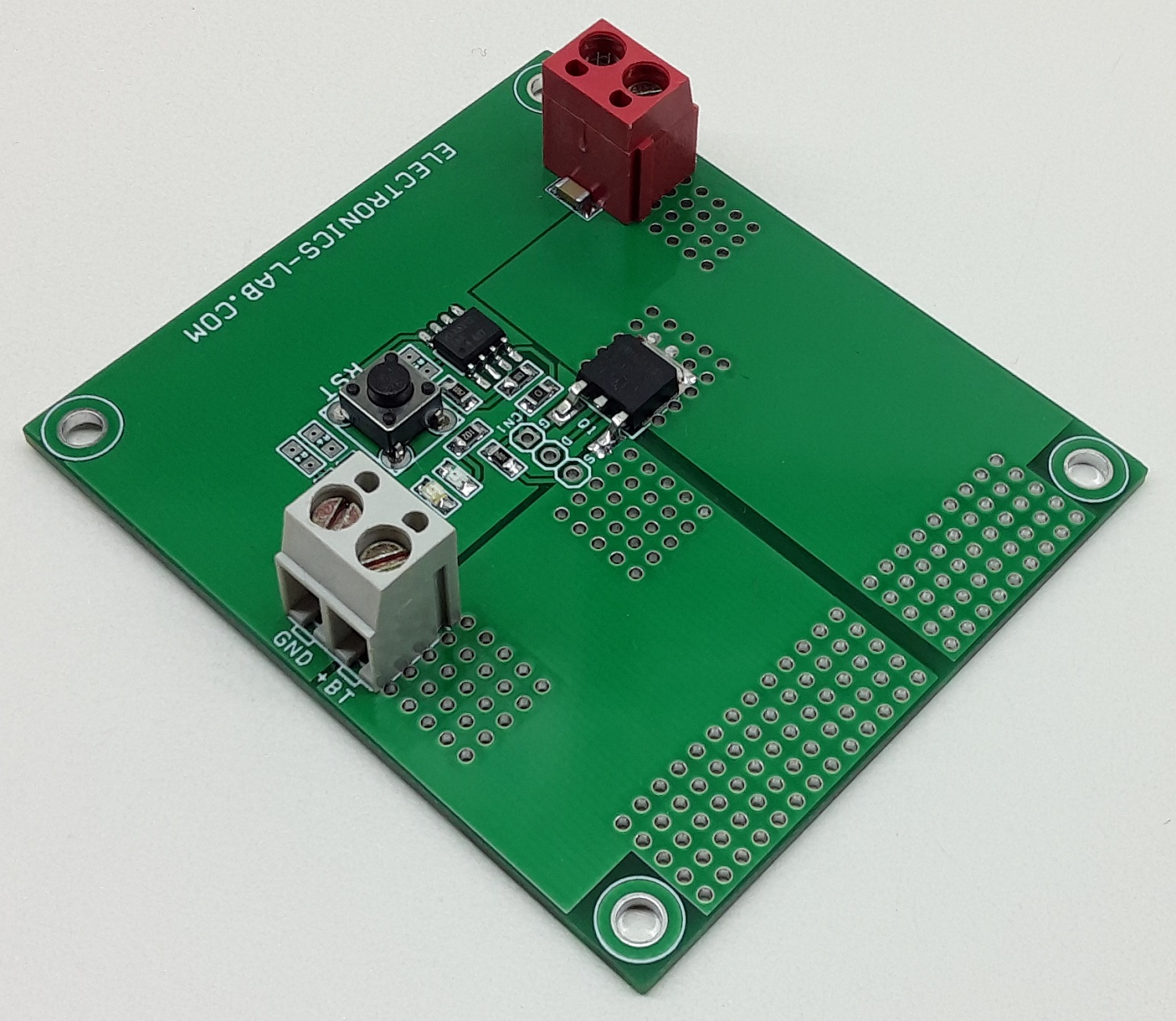
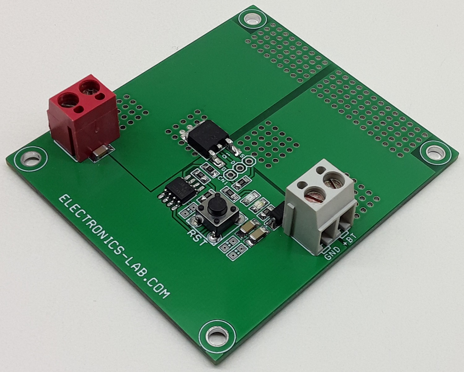
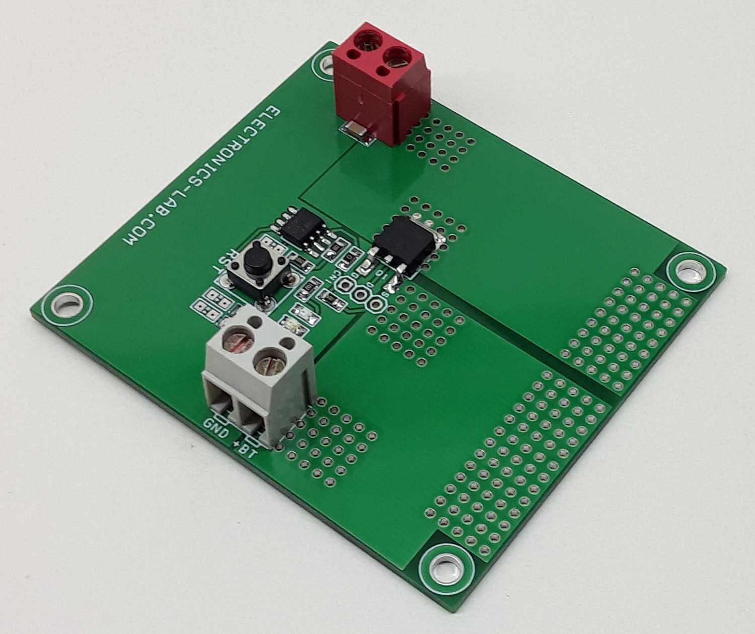
This project helps to optimize the 12V lead-acid (SLA) battery life as it prevents the battery from going into deep discharge. It is very important to disconnect the load before the battery enters into deep discharge as this may destroy or damage the battery cells. The circuit shown here turns off the load before the battery enters deep discharge and avoids a further (deep) discharge that can shorten the SLA battery life. Once the battery is recharged or replaced you need to push a reset switch to power ON the load. The predetermined load level is set to 12V, this voltage level is proportional to the battery voltage which is determined by resistor divider R2, and R9. Once the voltage falls below the setpoint (12V) it disconnects the load, the load-battery connection remains open until the system receives a manual reset command using tactile switch SW1.
The circuit drains 5uA + PWR LED D2 5mA, so the circuit can remain in that state for an extended period without causing a deep discharge of the battery. Users may not use LED D2 if not required. The circuit is capable to drive continuous load up to 5A and can provide more power with forced air cool to the MOSFET Q1. Connector CN1 is optional if the user wants to use TO220 MOSFET. The project is ideal for 1Ah to 10Ah 12V lead-acid batteries. Low ohm MOSFET is used to provide continuous maximum current output.
Note: Default Trip voltage (disconnect voltage) level is set to 12V, this can be changed as per user requirement. Use this formula to calculate the V-Trip voltage V-Trip=1.15V(R9+R2)/ R9
Features
Input Supply (12V Lead Acid Battery)
Continues Load up to 5Amps
Deep Discharge Disconnect Voltage Level 12V
Large size PCB thermal area provided for MOSFET for heat dissipation
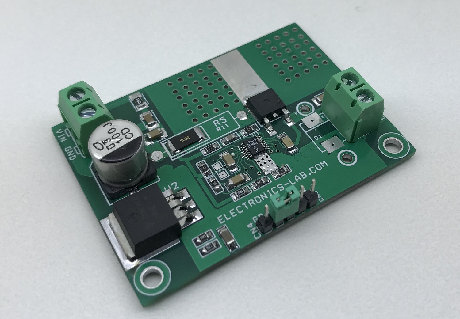
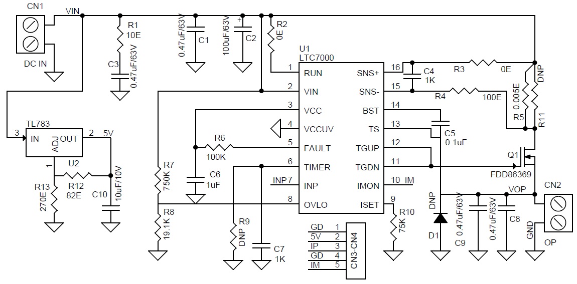
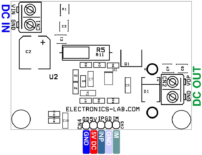
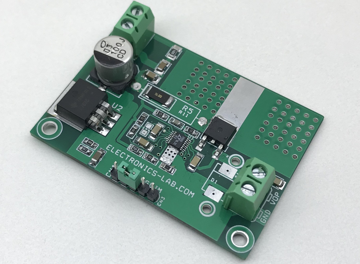
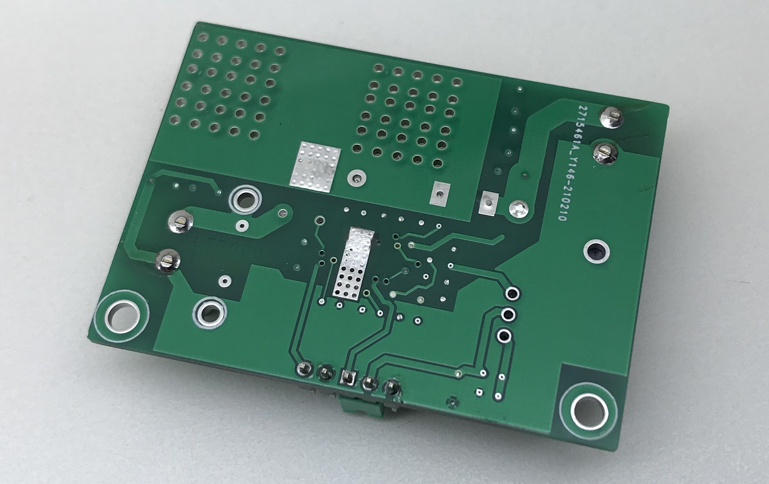
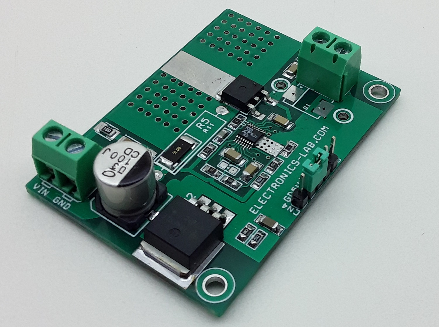
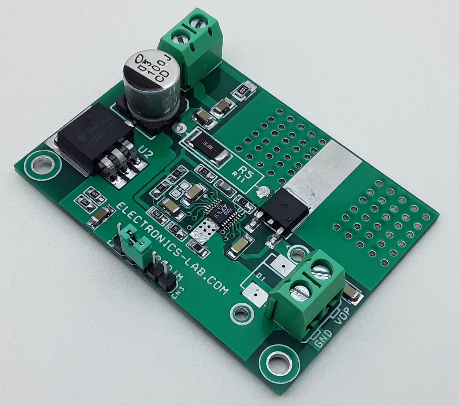
The project here is a 48V protected, high side switch designed to switch a 5A output load from input voltages from 8V to 48V. The circuit helps the user to easily ON/OFF the high current and voltage load with over-voltage lockout and over-current protection. The wide input range and low shutdown current (1μA typical) make it suitable for automotive, industrial, medical instruments, and telecom applications. This board offers a low 50ns (typical) propagation delay, fast switching times (<10ns), and 100% duty cycle operation. The project is based on LTC7000 which is a fast high voltage protected high side N-channel MOSFET driver. An internal charge pump fully enhances an external N-channel MOSFET switch, allowing it to remain on indefinitely. Its powerful gate driver can drive large gate capacitance MOSFETs with very short transition times, ideal for both high-frequency switching and static switch applications.
The circuit operates over an 8V to 48V input supply range. When an external current sense resistor and internal comparator sense that the switch current has exceeded a pre-set level, a fault flag is asserted and the switch is turned off after a period of time set by an external timing capacitor C7. After a cooldown period, it goes back on. The circuit is also configured to act when an overvoltage condition occurs. When voltage rise more than setpoint of 48V it switches off the output and remains off until input is cycled. Resistors R7, R8 are provided to set the overvoltage lockout, R10 sets the overcurrent limit, U2 5V is a regulator, Pin 3 (IMP) of CN3-CN4 provided to enable the output. This pin needs a High-level TTL-5V signal to enable the output, connect this pin to 5V to enable the output. When a fault condition occurs, disconnect the IMP pin from 5V and connect it to GND, pull up this pin to recycle the output.
Note: The project can be set for higher voltage and current, refer to the datasheet to configure the board for higher voltage up to 135V and current up to 10A.
Features
Supply 8V to 48V DC
Load Current 5Amps
Over Voltage threshold 48V
Easy On/OFF the high voltage and High Current Load
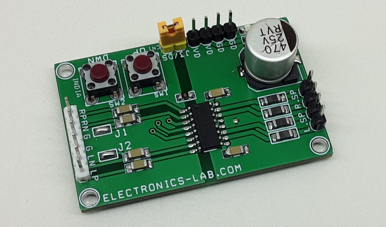
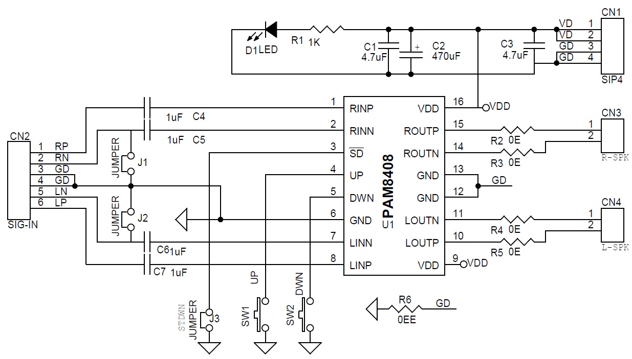
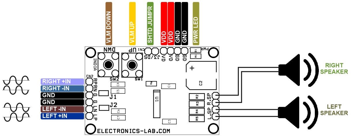
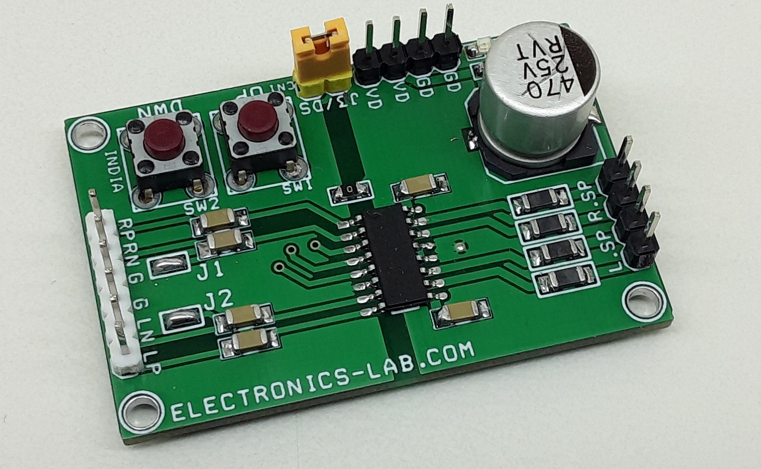
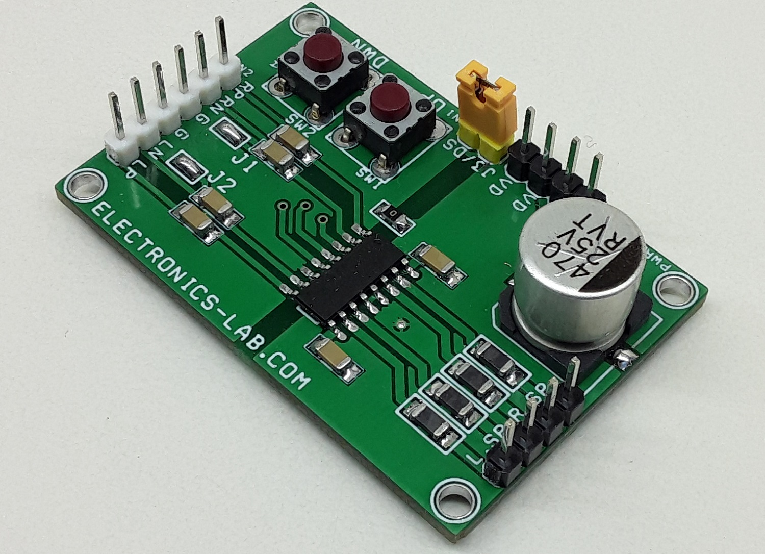
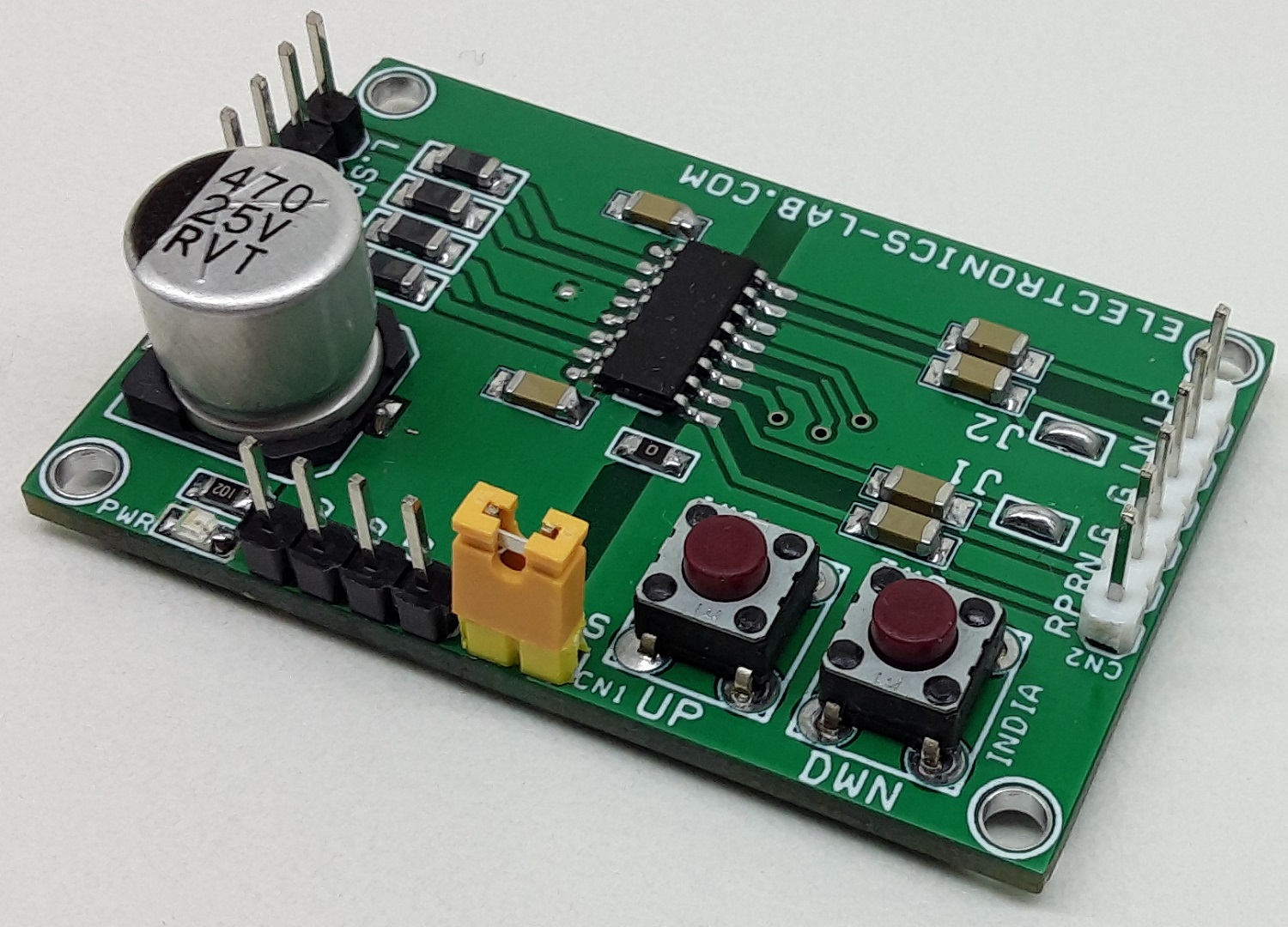
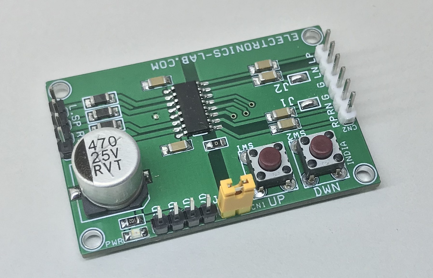
The circuit presented here is a 3W stereo audio amplifier with memory UP/DOWN volume control. The project is based on PAM8408 IC from Diode Incorp which is a filter-less class-D amplifier with high SNR and Differential input which helps eliminate noise. Two tactile switches are provided to control the UP/DOWN volume in 32-steps and it will hold the setting when the chip is in shutdown mode. The operating supply is 2.5V to 6V DC and this supply range helps to operate it with batteries like the use of 4 x Alkaline batteries. The small PCB size, 87% efficiency, low cost, minimum external components make this project ideal for portable applications. The PAM8408 also has built-in auto-recovery SCP (Short Circuit Protection) and thermal shutdown. The circuit works with differential audio signal input. It is advisable to use shielded wire for the audio input signals. Jumper J3 is open in normal operation, and if you close it puts the amplifier into shutdown mode and the audio volume will memorize when shutdown mode is recovered. Solder jumpers J1 and J2 are optional and of no use, it is advisable to keep these jumpers open. Connector CN1 is for power supply, CN2 is for audio signal input, CN3, and CN4 are for the speaker, Jumper J3 is for Shutdown, D1 is the power LED, Switch 1 increased volume, and Switch 2 decreases volume.
Volume changes are affected by toggling either the UP or DOWN tactile switches. After a period of 1 cycle pulses with either the UP or DOWN switch press, the volume will change to the next specified step, either UP or DOWN, and followed by a short delay. This delay decreases the longer the line is held low, eventually reaching a delay of zero. The delay allows the user to pull the UP or DOWN terminal low once for one volume change, or hold down to ramp several volume changes. The delay is optimally configured for push-button volume control. If either the UP or DOWN pin remains low after the first volume transition the volume will change again, but this time after 10 cycles. The followed transition occurs at 4 cycles for each volume transition. This is intended to provide the user with volume control that pauses briefly after initial application, and then slowly increases the rate of volume change as it is continuously applied. There are 32 discrete gain settings ranging from +24dB as maximum to -80dB as a minimum. Upon device power on, the amplifier’s gain is set to a default value of 12dB, and the gain will remain when Shutdown Jumper J3 is closed.
Features
Operating Power Supply 5V (2.5V to 6V Range)
2 x 3 W Power Output 4 Ohms Speaker @ 10% THD
Fully Differential Audio Signal Input for low noise operations
Onboard Shutdown Jumper J3
D1 Power LED
Ferrite Bead on outputs for Low EMI
32-Step Memory Up/Down Volume Control from -80dB to 24dB
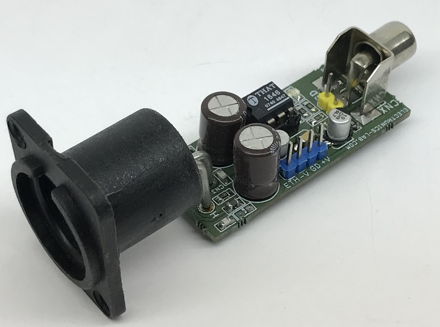
This audio-balanced line driver project enables to drive hundreds of feet in length of cables without becoming unstable The project is based on the THAT1646 chip, which is a new generation monolithic differential line driver that offers improved performance over conventional cross-coupled designs. Based on high performance, fully differential op-amp exhibits low noise and distortion, high slew rate, and wide output swing. Output is very stable when driving difficult loads, and output is short-circuit protected. The operating power supply is +/-15V DC, XLR, and RCA connector provided for output and input. D1, D2 are the Power LEDs, C7 decoupling capacitor, Ferrite Bead L1, L2, capacitor C6, C8, C9 take cares of RFI noise, Capacitors C5, and C10 acouple the common-mode feedback loop. This changes the loop operation from serving the common-mode output current at audio frequencies to serving the common-mode output voltage to 0 at DC. This results in much lower common-mode output offset voltage. D1 +VCC Power LED, D2 -VEE Power LED, CNX-J1 single-ended unbalanced audio input, CN3 Male XLR balanced audio output, CN1 power input, CN2 or J1-CNX audio input.
Audio-Balanced Line Driver – Unbalanced Audio to Balanced Audio Converter – [Link]
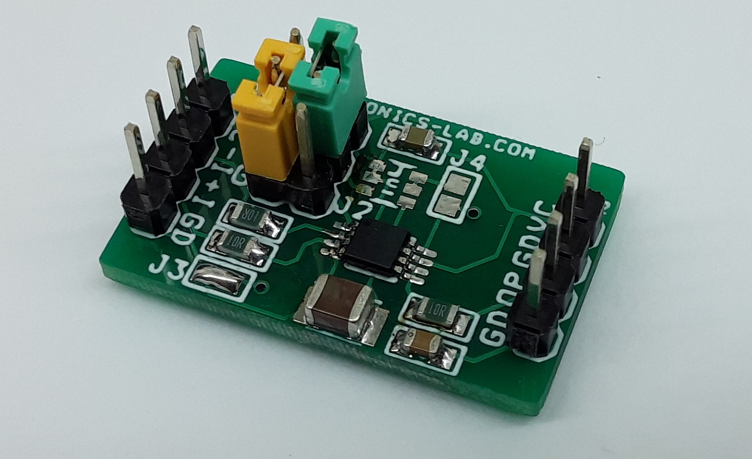
This board will make your work easy if you want to interface +/- 10V (Dual 10V) device or sensor to single-supply signal ADC. This tiny project has been made for industrial and process control applications and provides an easy interface between +/-10V (Dual 10V) sensor or device to single-supply ADC. Connect +/-10V sensor/device to pin 3 of connector CN1, and circuit outputs 0.5V to 4.5V at pin 3 of connector CN2. The operating supply of the circuit is 5V and it draws few milliamps of current. The project is also provided with optional precision Ref voltage for accurate output.
+/-10V (Dual 10V) to Single-Supply Signal Converter for ADC – [Link]