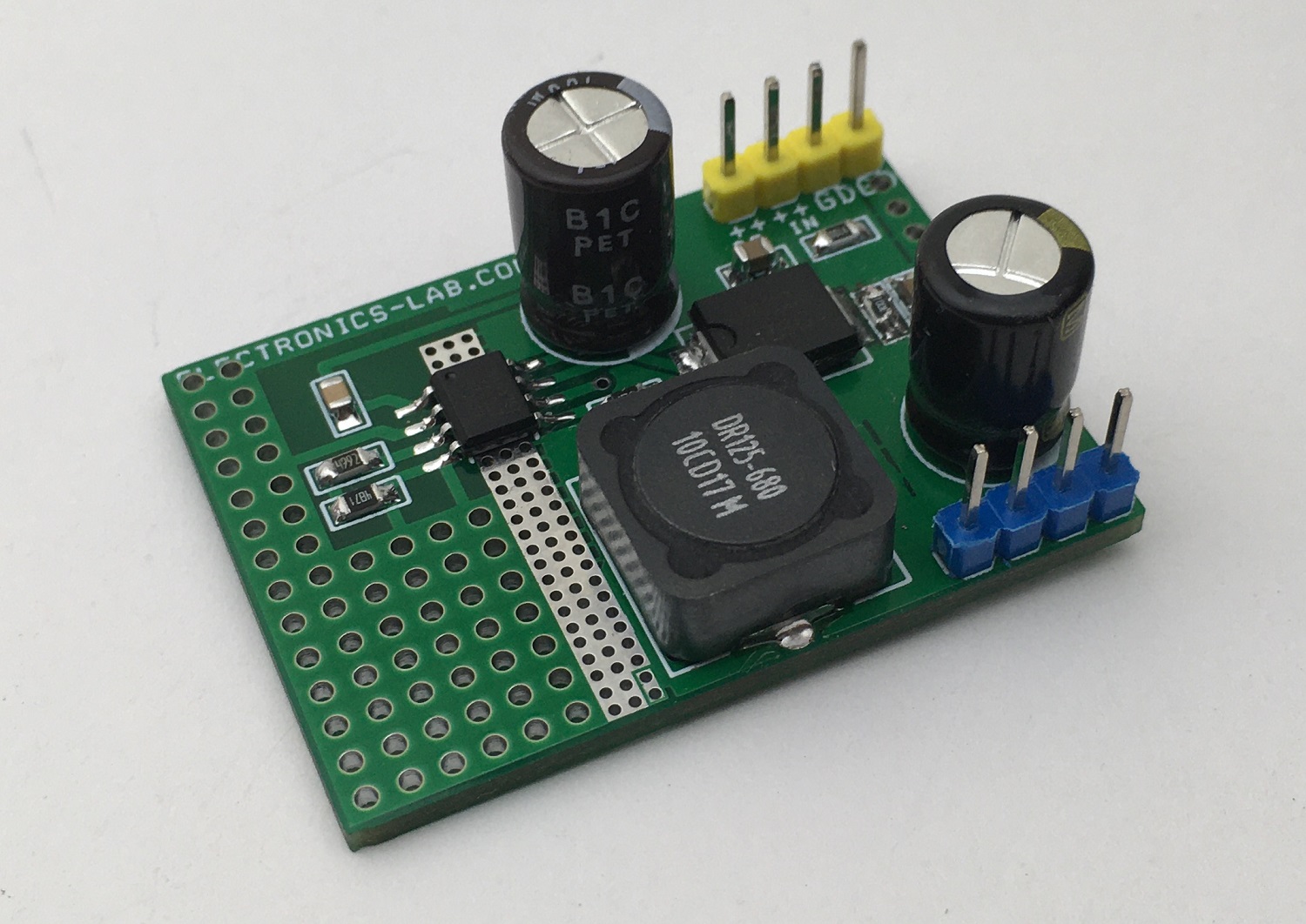
The project described here is a high voltage step-down regulator based on A4447 general-purpose buck converter chip from Allegro Semiconductor. The output voltage of the board is configured at 3.3V, but it is adjustable from 0.8 to 24V, based on the resistor divider R2 and R5. Connector CN1 is for DC input 24V-42V, Connector CN2 is DC Output. Refer to the information below to adjust various voltage outputs.
42V Input – 3.3V @ 2A Output High Voltage Step Down Regulator – [Link]
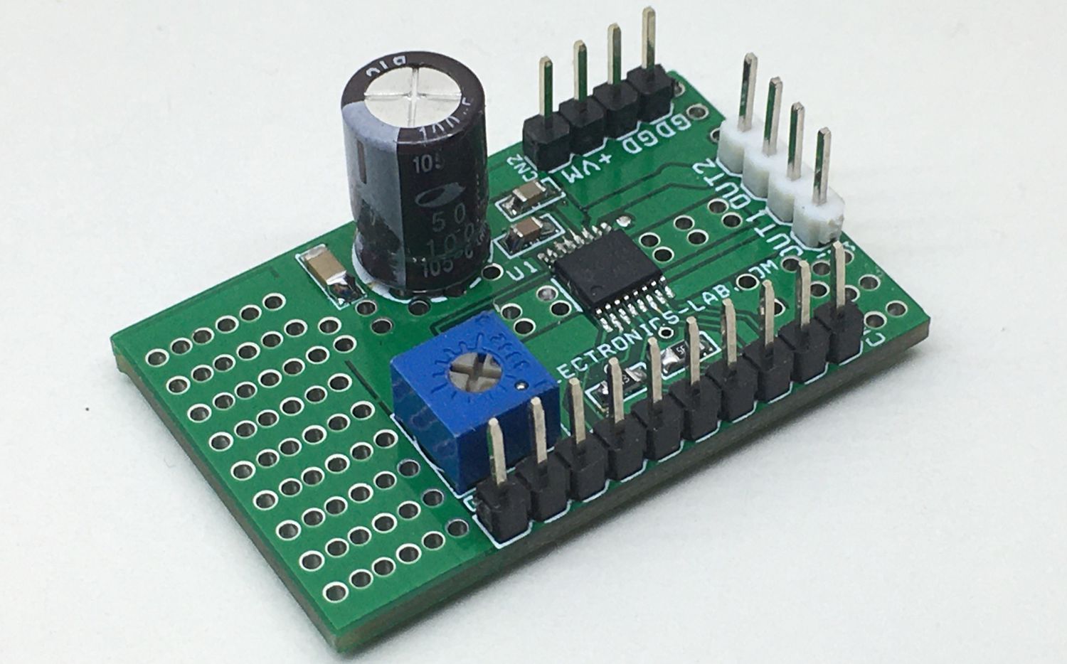
In past, we have published many brushed dc motor driver boards for various projects and usually, they have some sort of limitations, as some of them are large in size, require large size heatsink, doesn’t have current feedback, they don’t have overload protection, some require external large size current shunt resistor and after all, recently we have found the amazing DRV8874 chip from Texas instruments that has some amazing features and protections features. It has a small package and can handle high current without a heatsink. We quickly become fans of this chip, and after a few tests and experiments, we are sharing this open-source module. This chip can be used with PWM/DIR input, PWM input, and 2 x Half-Bridge for dual motor control. We have tested this project with PWM/DIR inputs, and all inputs and outputs of the chip are accessible using the header connector. Refer to the datasheet of DRV8874 to explore other features and configure the board as per requirement. Example Arduino code is provided below.
H-Bridge Motor Driver with Integrated Current Sense and Regulation using DRV8874 – [Link]
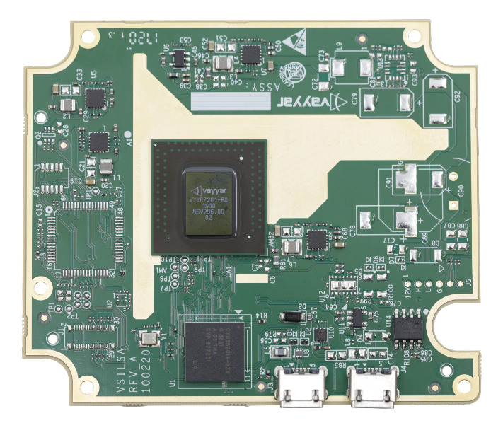
4D Imaging using radar technology provides good resolution and field of view for scanning applications. Vayyar’s single-chip platform is a good example, as it integrates multiple antennas using RoC for improved 4D Imaging.
The multifunctional single-sensor platform fulfills the Euro NCAP safety requirements using its 4D Imaging feature. The chip comes with 48 transceiving antennas on a single package, hence reducing the complexity and cost of the device. The 4D Imaging chip is compatible with various software for creating in-cabin safety applications. This includes child presence detection, seat belt reminders, and gesture detection.
The gesture detection by using the 4D Imaging chip follows the conventional method of radar imaging, with some additional techniques. The radiowaves cover a certain volume of space by transmission through multiple antennas for calculating direction and distances. The usage of multiple antennas can create a 3D structure. Additionally, the chip also enables analysis of the neighboring pixels by receiving the data on all receiving antennas. This creates real-time imaging of continuous 3D frames, hence allowing 4D Imaging.
Talking more about gesture detection, the real-time 3D frames are in motion if the person moves from the original position to a different position. The 4D Imaging chip is capable of scanning the data using 5 cm large pixels in the space. The system then matches the pattern of these pixels with the general gesture patterns. As, the device supports real-time imaging, so it can detect the change in gestures on a real-time basis as well. This is how gesture detection happens using the 4D Imaging technique.
Deployed 4D Imaging Single-Chip Platform
The device supports an
“end-to-end software-hardware platform that enables OEMs and Tier 1s to develop multiple advanced applications independently over its point cloud layer. Hence, these include Occupant Status (OS), optimized airbag deployment and dynamic disabling, seat belt pre-tensioning, eCall, vital signs, gesture recognition, out-of-position detection, intruder detection and more.”
The 4D Imaging chip supports the software compatible with 3D point cloud API, which allows multiple platforms to interface with the device. This opens up the option of creating customized applications, depending upon the requirements. The real-time generated data in the form of pixel patterns can operate for multiple functionalities and allows continuous development of the overall system.
As discussed above, the 3D and the real-time 4D data collected can be stored and processed for multiple use cases. This can include image processing and deep learning applications, as the data is available in huge amounts. Hence, the ML models trained on neural networks with the 3D data can be a novel approach. Hence, Vayyar’s single-chip platform featuring in-cabin safety features and gesture detection can initiate the integration of AI with Radar Imaging techniques.
For more information about the in-cabin platform, visit the announcement of the company. To know more about the 4D Imaging chip, one can visit the company website.
Before talking about OpenTitan and Microsoft Pluton – two security chips by two tech giants, let’s have an overview of what security chips actually are.
Today, the hardware-level security of an operating system is an extremely important matter and is taken very seriously by manufacturers. The core security of an operating system depends on a chip separate from the CPU. This chip is called TPM or Trusted Platform Module. TPM stores various keys and other sensitive information that saves the integrity of the entire system. Security chips are also used in embedded platforms where security is the utmost priority. A good example is IoT based smart home control system. If an attacker gets access to the secure keys of various APIs used for controlling “things” remotely, they can do anything. So, these types of keys are stored in TPM.
Silicon Root of Trust (RoT) chips can provide many security benefits by helping to:
Ensure that a server or a device boots up with the correct firmware and hasn’t been infected by low-level malware.
Provide a cryptographically unique machine identity, so an operator can verify that a server or a device is legitimate.
Protect secrets like encryption keys in a tamper-resistant way even for people with physical access (e.g., while a server or a device is being shipped).
Provide authoritative, tamper-evident audit records and other runtime security services.
Google OpenTitan
OpenTitan is the first open-source project building a transparent, high-quality reference design and integration guidelines for silicon root of trust (RoT) chips (such as TPMs). The main goal of OpenTitan is to make the silicon RoT design and implementation more transparent, trustworthy, and secure for enterprises, platform providers, and chip manufacturers. Big companies like Western Digital, Seagate, Nuvoton, etc. are partnering with Google in this project.
OpenTitan being open-source, Root of Trust chip designers can embed this in their design with little or no legal complexities. Also, numerous talented developers can contribute to this project and raise the security standard. Open-source silicon can enhance trust and security by design and implementation transparency. problems can be detected early, and bugs can be fixed. This will also provide implementation choices and preserve a set of common interfaces.
As per google, The OpenTitan project follows three key principles:
Transparency – anyone can inspect, evaluate, and contribute to OpenTitan’s design and documentation to help build more transparent, trustworthy silicon RoT for all.
High quality – we are building a high-quality logically-secure silicon design, including reference firmware, verification collateral, and technical documentation.
Flexibility – adopters can reduce costs and reach more customers by using a vendor- and platform-agnostic silicon RoT design that can be integrated into data center servers, storage, peripherals, and other devices.
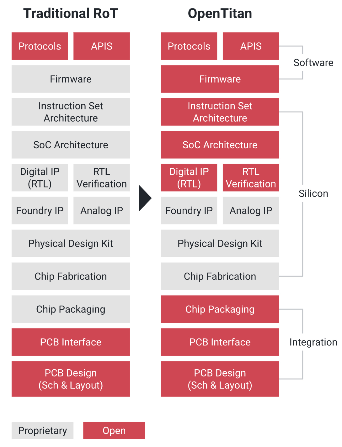
The following image shows the key differences between a traditional RoT design and OpenTitan:
Traditional vs OpenTitan
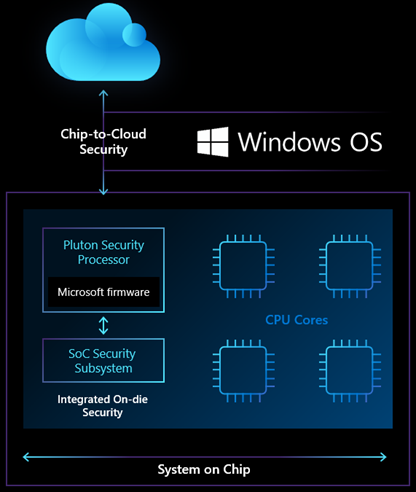
Microsoft Pluton
Even though TPM is the most commonly used RoT, there is one big problem – TPM lives outside of the main processor. An attacker with physical access to the computer can use a logic analyzer to steal information from the bus interface between the security processor and the main CPU. They can also modify the information using sophisticated attack techniques. So, with Pluton, Microsoft removes the potential for that communication channel to be attacked by building security directly into the CPU. In this way, it is almost impossible to tap the communication channel between the RoT and the CPU. Pluton is designed in collaboration with leading silicon partners AMD, Intel, and Qualcomm Technologies, Inc. So, processors made by these chip-designers will have Pluton security chip built-in.
Windows PCs using the Pluton architecture will first emulate a TPM that works with the existing TPM specs and APIs. This will enable customers to benefit from enhanced security for Windows features that rely on TPMs like BitLocker and System Guard. Even when an attacker has installed low-level malware or has physical access to the hardware, the secure information stored in Pluton cannot be removed. This is achieved by storing sensitive data like encryption keys securely within the Pluton processor, which is isolated from the rest of the system.
Microsoft Pluton
Conclusion
OpenTitan and Pluton have the same goal but with different philosophies. Both want to improve Root of Trust but google focuses to design an open standard for RoT design while Microsoft targets to embed RoT into the CPU to enhance Windows security. Both of them have the potential to be the future of security chips. Till now, neither OpenTitan nor Pluton has announced any specific processor that features either of them. Also, there’s is no release date available.
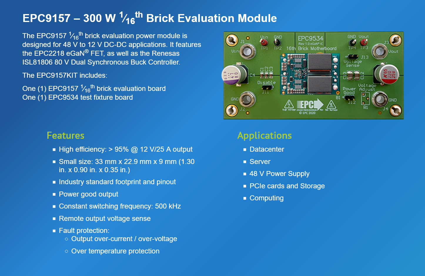
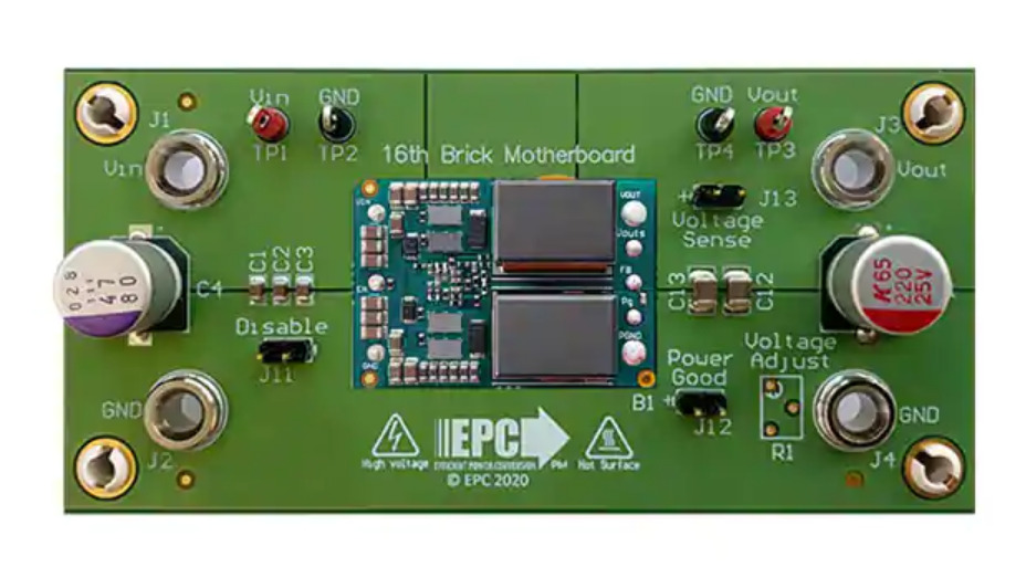
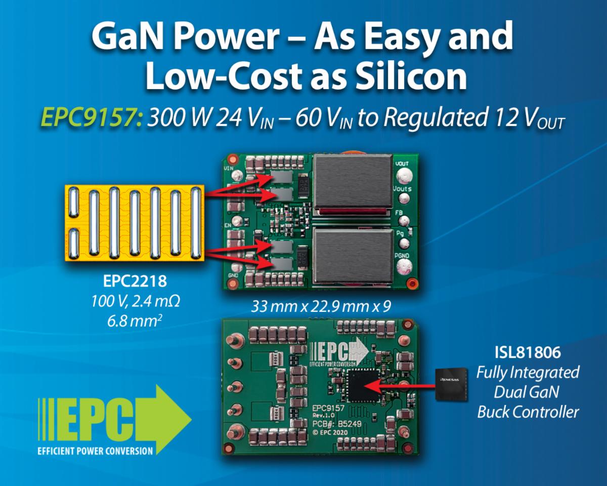
EPC announces the availability of the EPC9157, a 300 W DC-DC demo board in the tiny 1/16th brick size, measuring just 33 mm x 22.9 mm x 9mm (1.3 x 0.9 x 0.35 in). The EPC9157 demo board integrates the Renesas ISL81806 80 V dual synchronous buck controller with the latest-generation EPC2218 eGaN FETs from EPC to achieve greater than 95% efficiency for 48 V input to 12 V regulated output conversion at 25 A.
Brick DC-DC converters are widely used in data center, computing, telecommunication and automotive applications, converting a nominal 48 V to a nominal 12 V distribution bus, among other output voltages. The main trend has been towards higher power density. eGaN® FETs provide the fast switching, high efficiency and small size that can meet the stringent power density requirements of these leading-edge applications. EPC2218 is the smallest high efficiency 100 V eGAN FET on the market.
Renesas’ ISL81806 is the industry’s first 80V dual-output or two-phase synchronous buck controller with integrated GaN drivers, supporting switching frequencies up to 2 MHz. It uses peak current mode control and generates two independent outputs, or one output with two interleaved phases. It supports current sharing, synchronization for paralleling more controllers and/or more phases, enhanced light load efficiency, and low shutdown current. Protection features include input UVLO, over current, over voltage and over temperature. The ISL81806 can directly drive EPC GaN FETs, ensuring easy design, low component count and low solution cost. The highly integrated ISL81806 reduces BOM cost for GaN solutions because it does not require any microcontroller, current sense amplifiers, or housekeeping power.
Alex Lidow, CEO of EPC commented,
“Renesas’ synchronous buck controller IC makes using GaN even easier. We are delighted to work with Renesas to combine the benefits of its advanced controllers with the performance of GaN to provide customers with a low component-count solution that increases efficiency and power density and reduces system cost for 48 V power conversion.”
“The ISL81806 takes full advantage of the high performance of GaN FETs for high-power-density solutions while reducing BOM costs. It makes designing with GaN FETs as simple as using silicon-based FETs,” said Philip Chesley, Vice President, Industrial and Communications Business Division at Renesas. “We are excited to work alongside EPC to provide our customers with the latest in power conversion technology.”
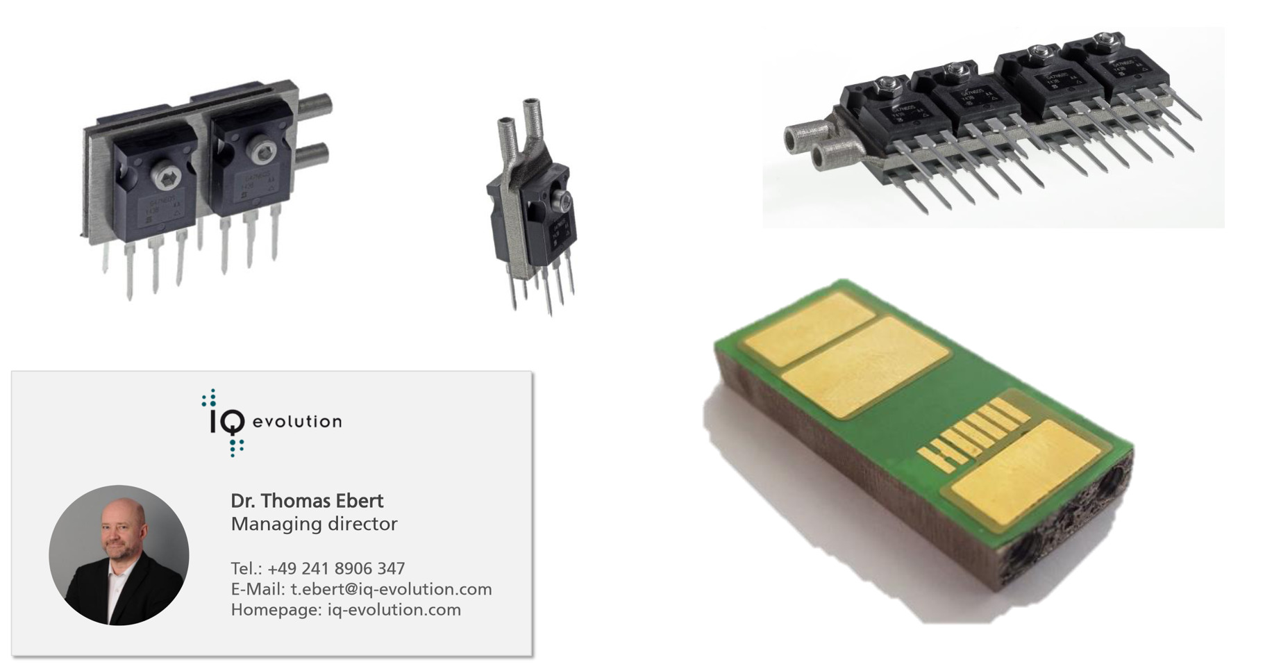
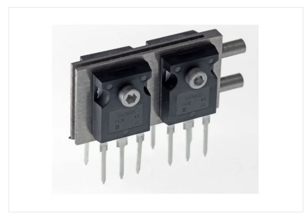
Standard Transistor Cooler Made by 3D-printing using SLM (Selective Laser Melting) A very effective way to dissipate the high heat flux densities of electronic power modules or power devices with high power density is the use of micro-coolers or micro-channel heat sinks made by SML. These active small cooling elements can transmit up to 1000 W/mm².Besides a design for the often used TO-247 housings, all other housing types are available. Even customized designs in other shapes and thicknesses are possible
The coolers are produced by SLM procedure, the Selective Laser Melting. The procedure is also known as LPBF (Laser Powder Bed Fusion).IQ evolution refined this 3D-metal-printing process over more than 10 years, especially to the requirements of building microstructures. Rapid Prototyping and completed mass production are both efficiently producible with this technology. For more information about the the3D-printing process please use our download-center: http://iq-evolution.com/downloads_de/
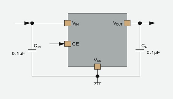
The XD6506 is a Voltage Regulator with ultra-low quiescent current, optimized for automotive applications. Consuming an incredibly low 0.8μA the XD6506 is the ideal choice for applications that require continuous, always ON operation. Furthermore, the CE function also allows the output of the regulator to be turned off, resulting in greatly reduced power consumption in standby mode.
The output voltage is selectable in 0.1V increments within the range of 1.2V to 5V using laser trimming technologies. The series is also compatible with low ESR ceramic capacitors, which give added output stability and the current limiter’s fold-back circuit also operates as short circuit protection for the output current limiter and the output pin.
The XD6506 is readily available in the industry-standard SOT25 package.
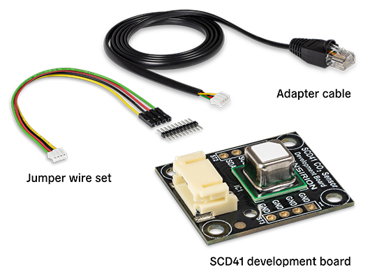
Sensirion SEK-SCD41 CO2 Sensor Evaluation Kit enables easy plug and play evaluation of the miniaturized SCD4x sensors and facilitates prototyping. Electrical interfacing can be realized either via the through-hole pads or alternatively via the included jumper cable that connects to the integrated JST connector. The compact design measuring 28mm x 24mm x 8mm, the large supply voltage range (2.4V to 5.5V), and the mounting holes allow versatile prototyping.
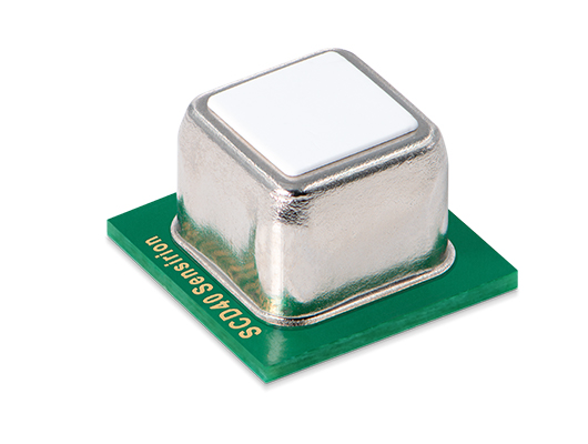
The SCD4x Miniature CO2 sensors build on the photoacoustic sensing principle and Sensirion’s patented PASens® and CMOSens® technology to offer high accuracy at an unmatched price in a small form factor. SMD assembly allows cost- and space-effective integration of the sensor combined with maximal freedom of design.
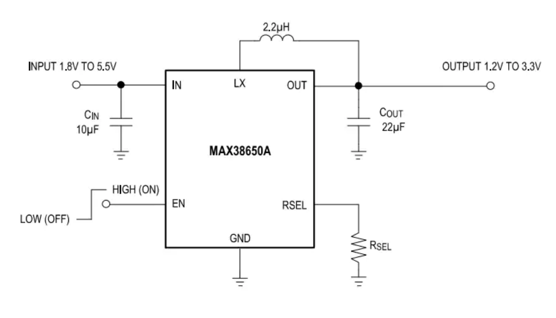
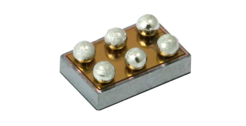
Maxim Integrated MAX38650 nanoPower Buck Converter provides an ultra-low 390nA quiescent current and operates from a 1.8V to 5.5V input voltage. The MAX38650 supports load currents of up to 100mA with peak efficiencies of 95%. The MAX38650 offers high efficiency throughout the load range with a small total solution size. The device is ideal for battery applications where extended battery life is required.
The Maxim MAX38650 nanoPower Buck Converter supports 100% duty cycle operation allowing seamless transition as battery discharges and falls below the target output voltage. The MAX38650 utilizes a unique control scheme that allows ultra-low quiescent current and high efficiency over a wide output current range.
The MAX38650 Converter is offered in a space-saving, 1.58mm x 0.89mm, 6-pin wafer-level package (WLP) (2 x 3 bumps, 0.4mm pitch), and is specified over the -40°C to +125°C operating temperature range.
Features
Extends battery life
390nA Ultra-low quiescent supply current
5nA Shutdown current
95% Peak efficiency and over 85% at 10µA
Easy to use addresses popular operation
1.8V to 5.5V Input Range
Single resistor-adjustable VOUT from 1.2V to 3.3V (MAX38650A)
Preprogrammed VOUT from 1.2V to 5V (MAX38650B) in steps of 50mV
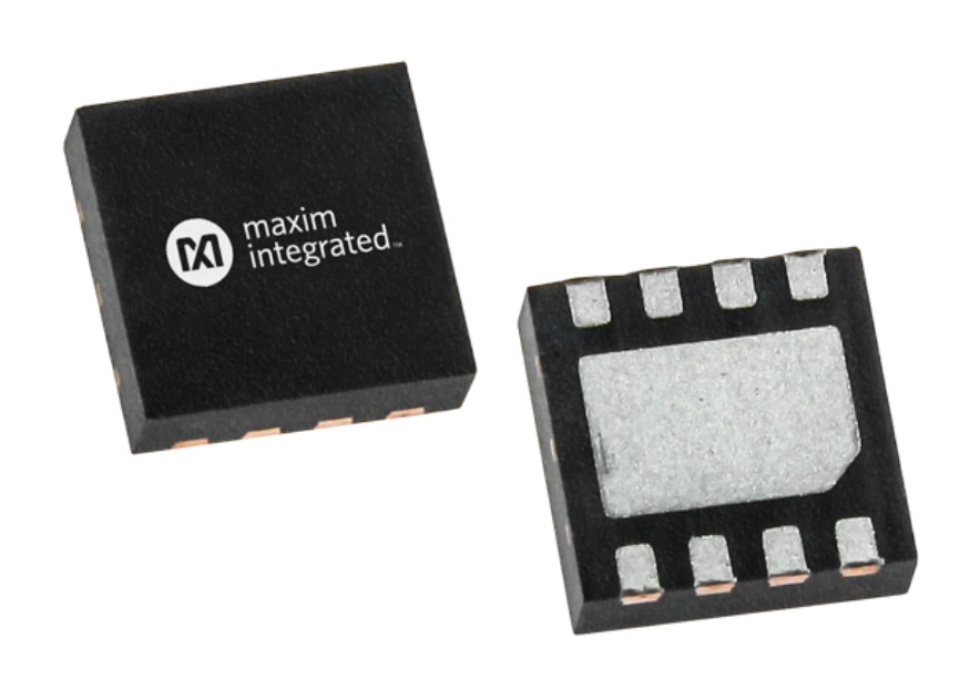
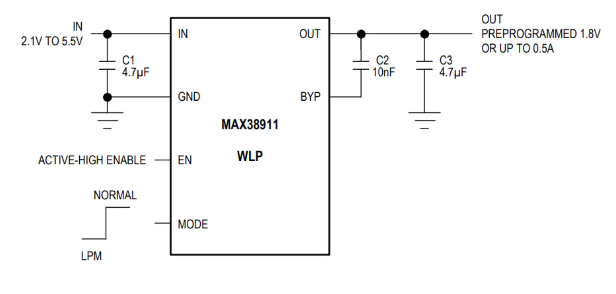
Maxim Integrated MAX38911 LDO Linear Regulators with low-power mode deliver up to a 500mA load current with only 11µVRMS of output noise from 10Hz to 100kHz.
The Maxim MAX38911 Regulators are set to have a single output voltage range of 0.8V to 5.0V. The output voltage on the MAX38912 is adjustable to a value range of 0.8V to 5.0V by using two external feedback resistors. The LDO Linear Regulators have protection features that provide programmable inrush current limiting, output overcurrent limiting, reverse current limiting, and thermal overload protection.
The MAX38911 is available in a 1.42mm x 0.83mm, 3 x 2, 6-bump, 0.4mm pitch WLP.
Features
Deliver wide, flexible operating range
1.7V to 5.5V Input supply range
0.8V to 5.0V Output voltage range
500mA Maximum output current
24.3mV Dropout at 500mA load and 5.0V input voltage
19.2µA No-load supply current in low-power mode
332µA Supply current in normal mode
<1µA Shutdown supply current
Reduce noise and improve accuracy
11µVRMS output noise, 10Hz to 100kHz
70dB PSRR at 10kHz, 250mA load current, and 300mV input and output voltage separation
±1% DC accuracy over load, line, and temperature variations
Enable ease-of-use and robust protection
Stable with 2µF (minimum effective) output capacitance