How To Build the Best PCB – JLCPCB

“Methods are more than difficulties”

It’s hard-won to run an industrial company. What’s the reason? One is the bosses who have earned money quickly expand their business footprint not only focus on PCB, not delve into how to provide higher-quality PCB and more extreme customer service; also many bosses think more about engaging in financing and listing. How about JLCPCB?Yes, JLCPCB has planted into the PCB with all its heart, just keeping one aim: build the PCB best.

JLCPCB was founded in 2006, used to be the leading PCB company, now it is PCB industry big brother, who is highly appreciated and trusted by hardware fields. When JLCPCB makes a mistake, people will say all they know without reserve. If the proposes will benefit the PCB users, JLCPCB takes act upon it without reserve. All we believe 15 years could build such solid and close relationship between customer and merchants. All suggestions and feedback from customers about production efficiency, PCB quality, customer service and logistics situation will be valued by JLCPCB team.

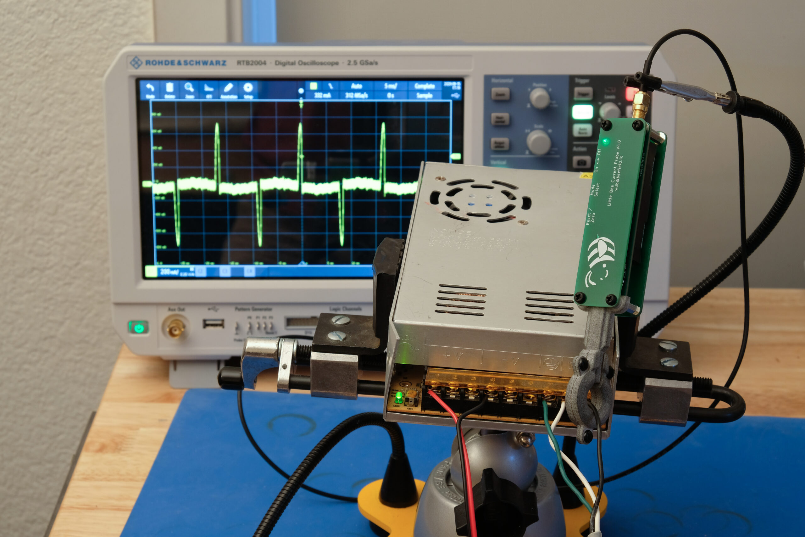
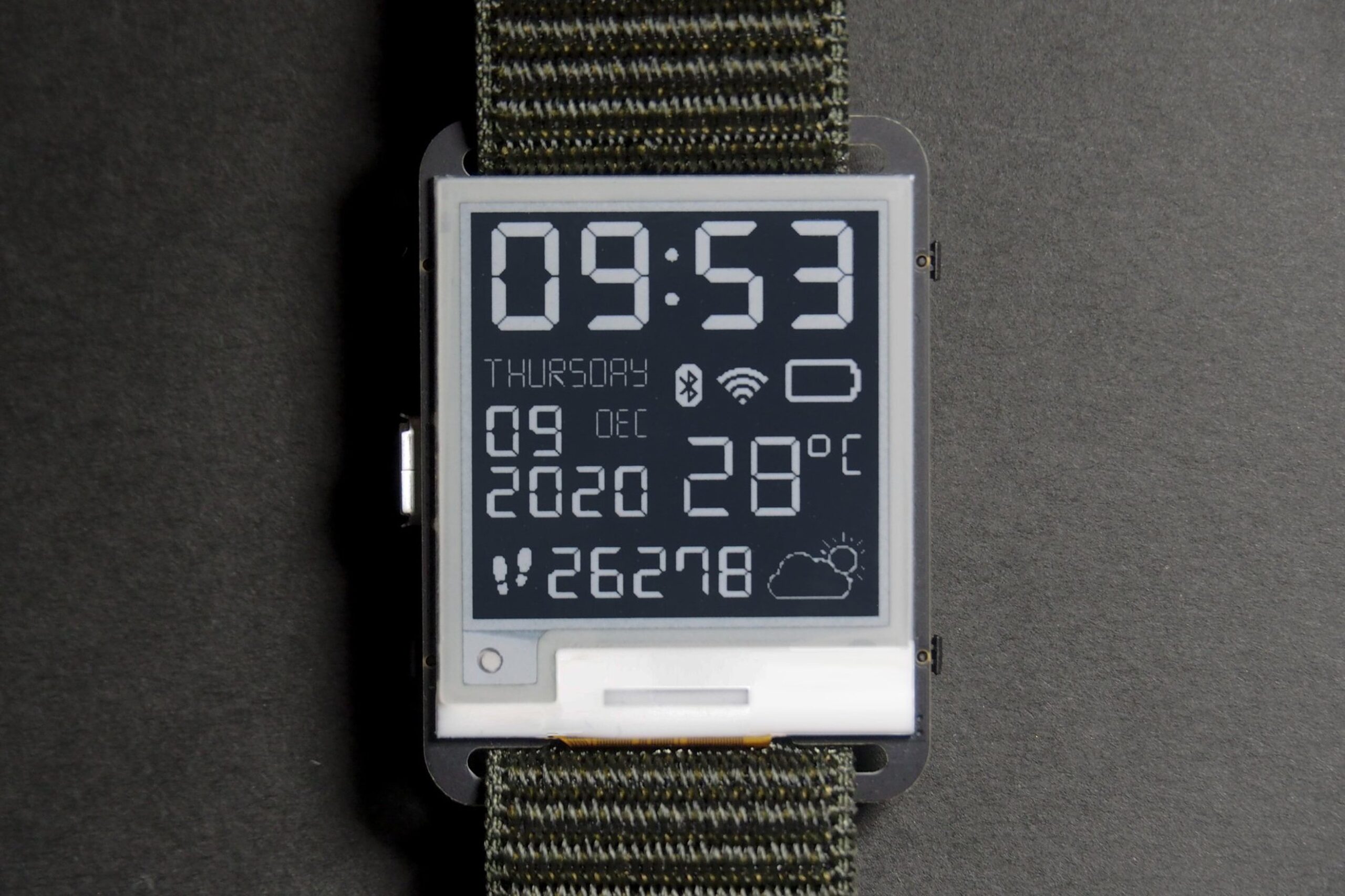
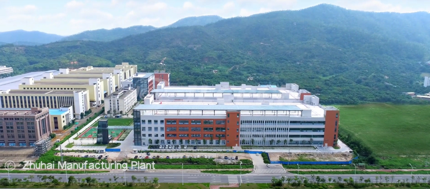
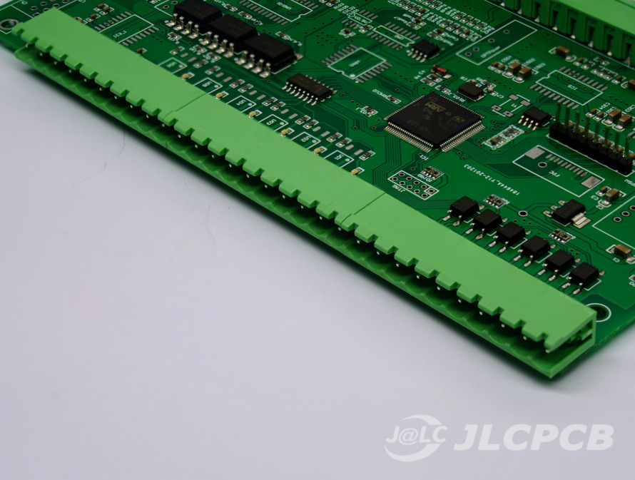
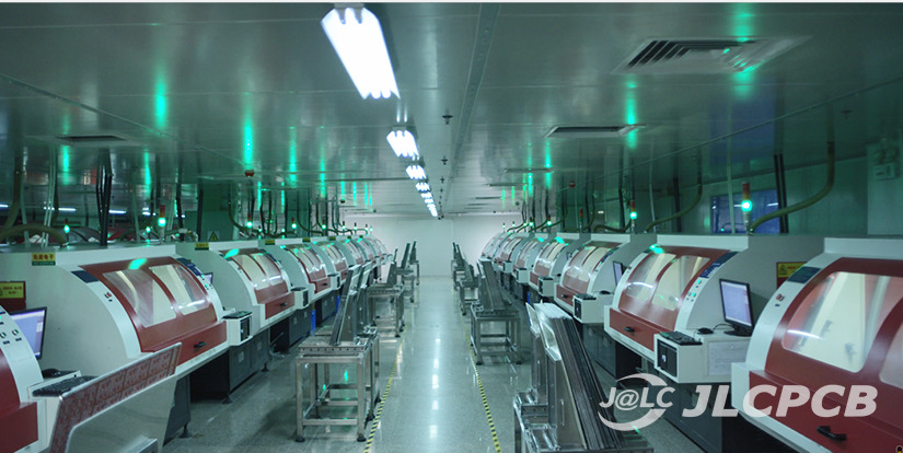
CEO Yuan was also a young electronic engineer before, and spent a lot of time in designing, developing, and testing components, devices and systems in a small PCB factory. Now he has grown up to be JLCPCB leader and is keen on optimizing and developing automatic production lines, intelligent factory management and brand new SMT assembly methods. He knows how sad it is for an electronic engineer to lack a good and inexpensive PCB board. His regret will not become the regret of a new generation of electronic engineers, so he insists on the PCB industry for more than 20 years, insists on low price but high quality PCBs for customers, and strives for excellence in craftsmanship and customer service. $2 for 5 PCBs, and $7 Start SMT assembly. Mr. Yuan elucidated, “The profit of the PCB industry is very transparent. Low price, superior quality, fast delivery. The essence is contradictory.” He added, “the only way to solve this contradiction: large production with the fully automated factory.” Yes, PCBs with high quality, low-cost and quick logistics must reach a certain scale of production to earn profits, 100% true. JLCPCB fully automated factory is indispensable. So far, it has 5 fully automated factories for 600,000 ㎡ per month, 9 SMT production lines 12-hour fast assembly 35,000,000+ parts monthly.

JLCPCB hopes to help engineers and companies to access most economic, best and innovative PCB service. We are trying to meet and exceed loyal users’ expectations in price, service and production. Even in 2020, it made these new attempts:

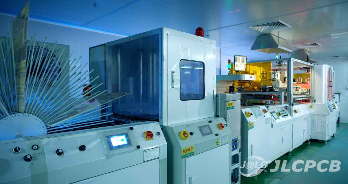
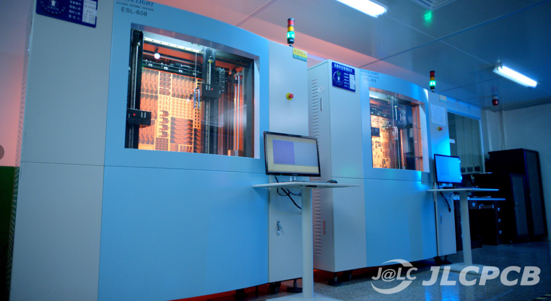
  • The SMT production plant was relocated to an advanced factory, expanding from the previous 32 machines to 72 placement machines;
  • expanded from the original 4 SMT production lines to 9 SMT production lines to support more production
  • Parts have increased from 30,000 kinds to more than 80,000 kinds
  • Added black, blue, red PCB assembly service

JLCPCB was also encountered many difficulties in Feb. 2020 because of the COVID-19 epidemic, which resulted in a bit longer PCB turnaround time and SMT order production delay. And the lead time has become as fast as before since March,2020. We redistributed the staff, and reorganized the equipment and manpower to make the production line run more and more smoothly. Of course, this is achieved when we ensure that our own employees are sufficient and well paid. That’s why we always say methods are more than difficulties.

Good products should be used by more people, especially people who desire high-standard hardware.For foreign customers, the first impression of JLCPCB is “$2 for 5 PCB” which has successfully entered the customers’ sight. People may curious about a “comprehensive JLCPCB” besides what they see online:where is the factory of JLCPCB ? What is the factory like? Who are the members of the JLCPCB team? Distance makes obstacles, however how JLCPCB shorten the distance with foreign customers.We would like to customize some small gifts randomly placed in the customer’s boxes. As the boxes flow to all corners of the world, people will receive our greetings. Little gifts are always appreciated and collected by the friendly users. For customers JLCPCB is a strong backer , thoughtful and caring. For JLCPCB, they are creative and productive talent.Their hardware projects promote the development of technology and are also changing people’s lifestyles and the pattern of the world.

Equipping and optimizing is JLCPCB 2021 target. JLCPCB are going to increase SMT part kinds, optimize the ordering process, and improve SMT quality while fastening turnaround time. In addition, it will add a 10,000 square meter plant with 100 SMT machines for small batch orders, also it can support double-sided SMT for any thickness. Every new attempt requires courage, and every “first” also requires more courage.JLCPCB, the first one to establish a fully automatic factory; the first to use the ERP system for online ordering; the first to cooperate with Alipay; the first to have ‘non-stop production in CNY holidays”. With a 15-year history, JLCPCB has taken every step steadily and will not waiver for any difficulties. JLCPCB believes building PCB best is the right way to gain customer retention.

Chinese New Year holiday is around the corner. JLCPCB users know that we keep production on holidays, even during the Chinese New Year Holidays. Certainly we will be here to serve everyone,1&2 layers PCBs, SMT assembly and Stencil will keep producing. Better late than never, we wish everyone a happy new year, stay healthy!

Video

MAX20361 Tiny Single-/Multi-Cell Solar Harvester works from 225mV

Maxim Integrated’s solar harvester increases runtime and reduces the size of solar-powered designs

Maxim Integrated’s MAX20361 is a fully-integrated solution for harvesting energy from single-/multi-cell solar sources. It has an ultra-low quiescent current (360 nA) boost converter that can start from input voltages as low as 225 mV (typical). To maximize the power extracted from the source, the MAX20361 implements a proprietary maximum power point tracking (MPPT) technique that allows efficient harvesting from 15 μW to over 300 mW of available input power. The MAX20361 also features an integrated charging and a protection circuit that is optimized for Li-ion batteries but can also be used to charge supercapacitors, thin-film batteries, or traditional capacitors. The charger features a programmable charging cut-off voltage with thresholds programmable through I²C interface as well as temperature shutoff. The MAX20361 is available in a 12-bump, 0.4 mm pitch, 1.63 mm x 1.23 mm wafer-level package (WLP).

Features

  • Efficient harvesting from 15 µW to over 300 mW of available input power
  • Maximum power point tracking (MPPT)
  • Battery/supercapacitor charger

Applications

  • Wearable fitness
  • Medical devices
  • Industrial IoT sensors
  • Asset tracking devices
  • Wireless sensor networks

more information: https://www.maximintegrated.com/en/products/power/battery-management/MAX20361.html

XENSIV™ Magnetic and Pressure Sensors

Infineon’s sensors enable innovative industrial as well as trend-setting consumer lifestyle applications

Infineon provides exceptionally precise magnetic sensors comprising industry-leading Hall switches, linear Hall, angle, 3D Hall, and current sensors as well as MAP and BAP pressure sensors. With more than 40 years of experience and a strong understanding of customer needs, Infineon has designed one of the broadest portfolio of sensor types on the market.

The Infineon manifold air pressure (MAP) sensor family is growing by adding two analog MAP sensors the KP212F1701 and KP212K1409, both dedicated for the two-wheeler market. Just like all other XENSIV™ MAP sensor families, KP212 features its proven high quality with a DPM rate lower than 0.3 DPM. These automotive-qualified analog pressure sensors are characterized by their high-precision pressure sensing: ±1.4 kPa at KP212F1701. The sensors offer dedicated transfer functions for two-wheelers.

XENSIV KP212F1701 Features

  • High-precision pressure sensing (±1.4 kPa)
  • Ratiometric analog output
  • Large temperature range: -40°C to +125°C
  • Broken wire detection
  • Clamping
  • Green 8 pin SMD housing, PG-DSOF-8-16
  • Automotive qualified, AEC-Q100

The TLI496x-xM integrated Hall-effect sensors are specially designed for highly accurate applications. The sensors provide an easy-to-use and cost-effective solution for position sensing applications, requiring high temperature stability of the magnetic threshold.

XENSIV TLI496x-xM Features

  • 3.0 V to 5.5 V operating supply voltage
  • Low current consumption: 1.4 mA
  • ESD protection 4 kV HBM
  • Active error compensation (chopped)
  • High stability of magnetic thresholds
  • Low jitter: typ. 0.35 µs
  • Operating temperature range: -40°C to +125°C
  • Small SMD package SOT23

The XENSIV TLI493D-W2BW 3D magnetic Hall sensor uses the latest 3D Hall generation from Infineon. The 3D sensor is housed in an extremely small wafer-level package. With an 87% smaller footprint and 46% less height than previous comparable products, the sensor opens additional design options for industry and consumer customers, such as joystick (e.g. finger, thumb and gaming paddles), mobile camera lens position sensing for focus and zoom, and much more. To complete the offering TLI493D-W2BW Shield2Go is available.

XENSIV TLI493D-W2BW Features

  • Component reduction due to 3D magnetic measurement principle
  • Small sensor form factor allows for very compact system designs
  • Wide application range due to high flexibility
  • Platform adaptability due to device configurability
  • Very low system power consumption due to wake-up mode
  • Disturbances of smaller stray fields are negligible compared to the high magnetic flux measurement range

more information: https://www.infineon.com/cms/en/product/sensor/pressure-sensors/absolute-pressure-sensors-map-bap/kp212f1701/

Adafruit’s Panel-mount TFT ESP32-S2 Wi-Fi Feather Board

TFT ESP32-S2 Wi-Fi Feather Board Top View

Adafruit has teased us with the announcement of the panel-mount TFT ESP32-S2 Wi-Fi Feather Board. It appears to be a succeeding version of the previous ESP32 Feather boards, by changing few positions of the components like the ESP32 module and USB-Serial converter, with the ESP32-S2-MINI module.

Apart from the NeoPixel in the schematic diagram, the STEMMA-QT header fits in the middle of the device. The four colorful dots indicate the vertical appearance of the connector. It serves the purpose of I2C as the larger JST PH connectors cannot fit on the compact feather board.

From the two Feather PCBs with ESP32-S2 SoC from the earlier devices, the panel-mount Wi-Fi Feather board has the TFT on the back and embedded with some tactile buttons. The TFT display makes the device quicker as it powers each pixel of the screen with a single MOSFET. TFT displays are mostly brighter than LCD displays.

TFT ESP32-S2 Wi-Fi Feather Board Bottom View

From the Twitter handle of Adafruit Industries, it can be understood that the company has been working on all-in-one-device. Hence, including a TFT display and WiFi on a single feather board. The design process of the device had started at the time of the creation of PyPortals, which was around 2 years ago now.

The company says “It started designing a low cost ‘mini PyPortal’ that would be able to run CircuitPython similar to those lilygo all-in-one esp32+display boards, but it did not have circuitpython running directly on the original esp32”

The Mini PyPortal

Mini PyPortal

The Feather M4 was experimented with using “ ESP32 + OLED into a panel-mountable design”, but it took a lot of space hence defying the purpose of miniaturization. The enhancement in the TFT technology since then opened up the opportunity to build things in a new way.

TFT ESP32-S2 Wi-Fi Feather Board features LC709203F, which is a fuel gauge for a single lithium-ion battery. The HG-CVR algorithm removes the use of a sense resistor and gives accurate RSOC information even under unstable conditions. Also, the feather board comes with a Li-ion battery charger. “This single-chip device is able to keep tabs on the trickle of charge flowing in and out of lithium cell.”

The TFT ESP32-S2 Wi-Fi Feather Board is still in the development process. However, Adafruit has given the option of contributing suggestions and features that could be included in the device. For more updates check out the Twitter thread of Adafruit Industries. Images and technical specifications have been taken from the Adafruit blog and Twitter thread.

DevEBox’s STM32H7XX-M Development Boards Features STMicroelectronics’ STM32H7 MCUs


STMicroelectronics’ STM32H7 series are a couple of Arm® Cortex®-M7-based MCUs that claim to deliver 1327 DMIPS and 3224 CoreMark. They come in three product lines- dual-core lines, single-core lines, and value lines, and can be used in the design of many rich and complex applications including wireless modules, alarm panel systems, power management systems, etc. 

To further the growth of the STM32H7 MCU series is China-based MCUdev DevEBox’s STM32H7XX-M development boards designed for factory automation, connectivity and security applications. These new STM32H7XX-M development boards are built around two different STM32H7 chips of a single-core line and a value line module. They have the same form factor and share similar features except for the difference in their core modules.

Specifications of the DevEBox STM32H7XX-M Development Boards:

  • Core Module:
    • STM32H743VIT6- Single-Core
      • 2048KB flash memory
      • 1024KB RAM
    • STM32H750VBT6- Value Line
      • 128KB flash memory
      • 1024KB RAM
  • Oscillator:
    • HSI: 64MHz
    • LSI: 32kHz
    • HSE: 25MHz
    • LSE: 32.768MHz
  • OLED interface: Plug and play, support 0.96″ / 1.3″ OLED
  • TFT liquid crystal interface:
    • Connect 1.3″ HD full color LCD
    • Connect 2.0″ HD full color LCD
  • 25MHz system crystal
  • 32.768KHz RTC crystal
  • 1x 10/100 Ethernet MAC
  • W25Q64 64Mbit QSPI Flash
  • 6x SPI, 3x I2S, 1x LPI2S, 4x I2C, 4x USART, 4x UART, 1x LPUART
  • 4x SAI, SPDIFRX, SWPMI, MDIO Slave, 2x SD/SDIO/MMC, 2x CAN
  • SWD header
  • 2x User buttons
  • 1x Reset button
  • Power and Programmable LED lights
  • 2.54mm integer double spacing pin
  • 8 to 14-bit Parallel Camera interface
  • 3x 16-bit 36-channel ADC
  • DCMI camera interface
  • HDMI-CEC
  • 1x temperature sensor
  • 2x DAC (12-bit)
  • 2x ULP comparators
  • 2x Op Amps
  • 1x high res timer
  • 2x 32-bit timers
  • 2x advanced timers
  • 10x general timers
  • 5x low power timers
  • 2x watchdogs
  • 96-bit unique ID
  • 2x USB OTG, 1x FS, 1x HS/FS
  • 1x Micro SD
  • M3 mounting holes
  • 3.3V LDO voltage regulator, max current 800mA
  • RTC battery header
  • Power Supply: Any +3.3V pin or +5V pin, and via USB connector (+5V).
  • Operating temperature range: -40 °C  to +85 °C
  • Dimensions: 40 mm x 68 mm

The STM32H7XX-M development boards are readily available and can be purchased either on Aliexpress or on Banggood. You’ll get the STM32H750VBT6 module board for $10.92 and the STM32H743VIT6 for $18.20.

Just like other core modules from STMicro, the STM32H7 series also comes with complete software support of Arm Cortex-M architecture. You can use the STM32CubeH7 full embedded software package, which comes with several examples for the STM32H7 series.

User manuals specific to the boards are available on the banggood link mentioned above, while further details on the STM32H7 MCU series including a getting started guide can be found on the STMicroelectronics’ website.

e-con Systems announces 90fps 4K SONY STARVIS® Camera with ultra-low light performance

SONY STARVIS IMX415 Sensor | Ultra-HD 4K Resolution |High Frame Rate (90fps) at 4K |NVIDIA Jetson Xavier NX/Nano

e-con Systems Inc., a leading embedded camera solutions company, brings its new SONY STARVIS based 4K Ultra-HD MIPI camera module to the market for smart city, sports vision, quality inspection and factory automation applications.  This camera module is suitable for applications requiring high level of image recognition and detection with a compact design, which makes it suitable for video analytics purposes. The new 4K camera module, e-CAM83_CUMI415_MOD adds to e-con’s 4K (Ultra-HD) family of cameras with its unique 90fps streaming capability. This camera comes with the 8MP SONY STARVIS® IMX415 CMOS image sensor. Its low light sensitivity delivers clear color images even at extremely low light or even no light (nearly 0 lux) conditions. It is capable of streaming high frame rate (90 fps) at 4K (3840 x 2160) resolution. Its interchangeable M12 (S-mount) lens allows customers to choose the lens of choice according to their application needs.

“Next generation of Smart Surveillance cameras powered by NVIDIA Jetson, demand high resolution 4K video for monitoring of large area and our e-CAM83_CUMI415_MOD will be the ideal camera for these applications thanks to its excellent low light capability and 4K video streaming. The first-in-the-segment feature of 4K streaming video at 90 fps Jetson AGX Xavier platform marks e-CAM83 as an ideal solution for AI sports cameras, drone camera photography and many applications requiring high resolution and high frame rates.“

said Ashok Babu, President of econ Systems, Inc.

The 4K camera provides four times the resolution of 1080p, delivering exceptional image details with good color reproduction, which is ideal for applications that require monitoring a huge area such as parking lot management, traffic monitoring systems, smart surveillance etc. The ability to stream 90 fps in uncompressed format along with its low light performance make the product suitable for industrial applications such as factory automation and quality inspection as well.

To accelerate product development for the above applications, evaluate the e-CAM83_CUMI415_MOD camera module. e-con Systems offers camera evaluation kits with both MIPI and USB interfaces,

  • MIPI evaluation Kit – e-CAM80_CUNX – plugs into the NVIDIA® Jetson Xavier NX™ developer kit.
  • USB evaluation kit – e-CAM82_USB – USB 2.0 UVC compliant camera

(Note: e-CAM80_CUNX uses NVIDIA’s Jetson internal ISP for image processing)

Low Light Images

The color images captured at 0.4 lux and 2.5 lux using e-CAM80_CUNX MIPI camera kit are given below:

e-CAM80_CUNX – SONY STARVIS IMX415 MIPI Camera at 0.4 lux
e-CAM80_CUNX – SONY STARVIS IMX415 MIPI Camera at 2.5lux

Video

Availability

Customers interested in evaluating the 4K MIPI camera module with NVIDIA® Jetson Xavier™ NX developer kit can purchase e-CAM80_CUNX from e-con Systems’ online store.

For buying the USB evaluation kit, please write to us at camerasolutions@e-consystems.com

Customization Services

e-con Systems also offers extensive customization services and integration support for e-CAM83_CUMI415_MOD if needed. If you are looking for any additional features or customization, please contact us at camerasolutions@e-consystems.com.

XDL601/02 – 5.5V, 1.5A Hi-SAT COT Synchronous Buck Micro DC/DC with integrated Coil

The XDL601/02 are ultra-small, 1.5A, synchronous step-down Micro DC/DC Converters with integrated inductor and high-speed transient response. The superfast load transient performance is due to Torex’s innovative Hi-SAT COT control method, which, when compared to standard Constant On-Time (COT) control also provides less fluctuation in oscillation frequency against load and input voltage.

The XDL601/02 total solution size is only 30mm2 and is optimised for space constrained applications such as sensors, cameras, small control modules, telematics, infotainment & HMI.  The XDL601 operates with Hi-SAT COT plus fixed PWM mode with a 3.0MHz switching frequency whereas the XCL602 automatically switches between PWM and PFM (pulse-skipping) mode to maximize efficiency at lighter loads.

The input voltage range is 2.5V to 5.5V and the output voltage range is 0.8V to 3.3V (accuracy ±2.0%). The operating ambient temperature range is -40°C ~ 105°C and this series is AEC-Q100 Grade 2 compliant. In addition, Thermal shutdown, integral soft-start and a built-in UVLO function are also included for added protection.

The XDL601 is available in a small DFN3625-11B (3.6 x 2.5 x 1.6mm) package which has Wettable flanks.

Key features

  • Operates from 2.5V to 5.5V
  • Up to 1.5A Output Current
  • Output Voltages from 0.8V to 3.3V
  • Hi-SAT COT with PWM Control or PWM/PFM Auto-Switching
  • AEC-Q100 qualified (-40˚C ~ +105˚C)

Key benefits

  • Integrated Coil Structure
    • More than 50% of PCB Area Savings
    • Minimized Radiated Noise (EMI)
  • High Efficiency at 3.0MHz Operation
    • 93% (at VIN=5.0V, VOUT=3.3V/500mA)
  • Enhanced COT Technology
    • Fast Transient Response
    • Stable Frequency Operation
    • Superior Load Regulation
  • High Reliability
    • Exposed Flanks Package
    • High Thermal Performance

more information: https://www.torexsemi.com/products/built-in-dcdc-converters/series/?name=xdl601

XD9260/61 – 1.5A Hi-SAT COT Synchronous Step-Down DC/DC Converter

XD9260/61 – 1.5A Hi-SAT COT Synchronous Step-Down DC/DC Converter, AEC-Q100 compliant

The XD9260/XD9261 series is a small 1.5A synchronous step-down DC/DC converter with high-speed transient response and low quiescent current. The extremely fast load transient performance is a result of Torex’s innovative Hi-SAT COT (Constant On-Time) control method, which, when compared to standard Constant On-Time (COT) control, provides less fluctuation in oscillation frequency against load and input voltage.

The input voltage range is 2.7V to 5.5V and the output voltage range is 0.8V to 3.6V (accuracy ±2.0%). 1.2MHz or 3.0MHz can be selected for the oscillation frequency and the operating ambient temperature range is -40°C ~ 105°C.

The XD9260 operates with Hi-SAT COT plus fixed PWM mode with fixed switching frequency whereas the XC9261 automatically changes between PWM and PFM (pulse-skipping) mode to maximise efficiency at lighter loads.

The soft-start time is set to 0.3ms (TYP.). With the built-in UVLO function, the driver transistor is forced OFF when the input voltage becomes 2.0V or lower.

Key features

  • Input Voltage from 2.7 V to 5.5 V
  • Output Voltage from 0.8 V to 3.6 V in 0.05 V increments
  • Up to 1.5 A Output Current
  • Low Quiescent Current, only 15 µA (1.2 MHz)
  • AEC-Q100 qualified (-40 ˚C ~ +105 ˚C)

Key benefits

  • Space Saving Solution
    • Ultra-Small USP-6C Package (2.0 x 1.8 mm)
    • Small-Value Inductor (1.0 µH)
    • Minimized External Component Count
  • Ultra-Low IQ and High Efficiency at Light Load Conditions
    • 15.0 µA in Sleep Mode
    • 0.1 µA in Shutdown Mode
  • Hi-SAT COT Control
    • Ultra-Fast Transient Response
    • Stable Switching Frequency​

more information: https://www.torexsemi.com/products/step-down-dcdc-converters/series/?name=xd9260

Little Bee, affordable high-performance current & magnetic field probe

A campaign for a current probe called Little Bee was launched on Crowdsupply. Little Bee is an affordable and high-performance current probe and magnetic field probe that enables you to debug and analyze electronic devices more effectively. This device comes in handy because current probes available today are expensive, therefore having a limited number of users. Current probes are gaining ground today because of the popularity of power electronics like electric vehicles, alternative energy, and high-efficiency power supplies. Regarding the aim of the project, the company says:

“We hope to make the world of power electronics accessible to more people by delivering a much-needed piece of test equipment as open hardware and at an affordable price.”

Little Bee can function as a traditional current probe, providing isolated measurements of the current in a wire with higher accuracy, and It can also measure currents over a wide bandwidth: from DC to the MHz range. Thanks to its Anisotropic Magneto-Resistive (AMR) magnetic sensor, Little Bee’s performance can be compared to other current probes based on fluxgate magnetometers, and probes with hybrid features that offer AC current transformers with DC hall effect sensors. Little Bee offers the same level of performance, but with a much lower cost.

The AMR sensor functions by sensing magnetic fields, producing a voltage proportional to the magnetic field strength. It features a clip, which enables current sensing by translating the current in a wire into a magnetic field. It is also equipped with a ferrite toroid with an air gap in which the sensor tip rests. The synergy between the current in the wire and the magnetic field in the air gap varies little as the wire moves around the center of the toroid. This enables accurate current sensing despite variations in the test setup.

The output of the AMR sensor is amplified by low noise, high bandwidth amplifier to provide the correct signal level for oscilloscopes. The amplifier is controlled by a PIC microcontroller, enabling automatic zeroing and offset adjustment as well as gain and bandwidth switching. Little Bee is easy to use. It can connect to any oscilloscope with a standard 1 MΩ input impedance via the provided SMA to BNC cable. You don’t have to carry out much configuration, it is ready for use, you just flip the power switch and it comes on. It features two buttons that are used to zero the probe and to cycle through bandwidth and gain options.

About accessibility, the company says:

“It is important that the open source community have access to high-quality tools. A desire to make a once prohibitively expensive technology accessible to a wider audience inspired the creation of the Little Bee. All the project files are hosted on GitHub under the Creative Commons Attribution-ShareAlike 4.0 license.”

Production will be carried out in different parts. The main Little Bee PCB will be assembled by MacroFab situated in USA, and the mechanical parts will be 3D printed out of Multijet FusionPA12 by Sculpteo. Also, the final mechanical assembly of the probe, firmware flashing, and calibration, will take place in-house before shipping all finished units to Crowd Supply’s fulfillment partner Mouser Electronics, who will distribute them to backers.

Features

  • Adjustable bandwidth (10 MHz and 1 MHz)
  • Adjustable gain (1x and 4x)
  • SMA Output Connector
  • Connects to any standard 1 MΩ impedance oscilloscope input
  • Powered by a single AA battery (4 hour battery life)
  • Automatic zeroing
  • Bandwidth: DC – 10 MHz
  • Sensitivity: 0.25 Volts/Amp
  • Max Current: +/- 5 A
  • Noise
    • *3 mA RMS at 10 MHz bandwidth
    • *2 mA RMS at 1 MHz bandwidth
  • DC Accuracy: +/- 15%
  • Insertion Impedance: 100 nH in parallel with 70 Ohms
  • Maximum Wire Size
    • *4.25 mm unbroken
    • *10 mm end-fed
  • Magnetic Field Sensing
  • Bandwidth: DC – 10 MHz
  • Sensitivity: 0.2 Volts/Gauss
  • Max Field: +/- 6 Gauss
  • Noise
    • *4 mG RMS at 10 MHz bandwidth
    • *2.5 mG RMS at 1 MHz bandwidth

This is a project by Weston Braun who is a Ph.D. Student in Power Electronics at Stanford University. More information can be found in Crowdsupply.

Watchy: Pebble-like SmartWatch with Bluetooth and WiFi 4 Connectivity

The Watchy e-paper smartwatch reminds us of the Pebble e-paper smartwatches, which came with a Bluetooth interface for connection with personalized Android and Apple mobile handsets. It used to support SDK for customization of the features according to the user requirements. However, the Pebble had closed its smartwatches after the Fitbit acquired the company in 2016.

Watchy seems to be a closer resemblance to Pebble-like smartwatches, but instead of a full-color OLED display, it comes with a monochromatic 1.54-inch e-paper display. The screen has a resolution of 200 x 200 pixels and is offcource low power. Hence, this makes the Watchy smartwatch readable from different viewing angles. Although, it has one drawback that it does not include a backlight or sidelight for seeing time in the dark.

Key Features of Watchy Smartwatch:

  • Microcontroller ESP32-PICO-D4
  • USB-Serial CP2104
  • E-Paper Display GDEH0154D67
  • Display Connector AFC07-S24ECC-00
  • 3-Axis Accelerometer BMA423
  • Real-Time Clock DS3231
  • Battery LiPo Battery 3.7V 200mAh 402030
  • LDO Voltage Regulator ME6211C33M5G-N
  • Battery Connector BOOMELE 1.25T-2PWT
  • Micro USB Connector U-F-M5DD-Y-L
  • Tactile Buttons K2-1114SA-A4SW-06
  • Vibration Motor 1020
  • PCB Antenna SWRA117D

Watchy comes with Espressif Systems ESP32-PICO-D4 system-in-package with ESP32 dual-core processor with Bluetooth LE 4.2/5.x and WiFi 4 connectivity. It also features wide viewing angles and 4MB SPI flash for interfacing. BMA423 is the 3-axis accelerometer functioning as a sensor for gesture detection and activity tracking. Talking about the power specification, it has a 200 mAh battery fit for 5-7 days for timekeeping provided without WiFi. Whereas with a WiFi connection it can only last 2-3 days.

“The Watchy library depends on other open source libraries to drive all of its hardware, some of which have been wrapped in Watchy.h to provide a framework for building watch faces and apps.”

Watchy supports GxEPD2 which is an Arduino Display Library for SPI E-Paper Displays. Also, It works with SPI communication needed to control Watchy’s E-Paper display. This library depends on the Adafruit GFX library, which provides the graphical interfacing methods for customized images, shapes, and text. It also allows functions such as a display.drawRect() for drawing shapes, display.drawBitmap() for drawing images.

Watchy’s software, hardware, and documentation are fully open source under MIT license and OSHWA certified. Watchy smartwatch is available on Tindie for $49.99 but at this point in time, it is out of stock. You can still register your email address to join the waiting list to purchase the smartwatch in the next lot. Images and technical specifications have been taken from Tindie’s blog and Watchy’s documentation.

TOP PCB Companies