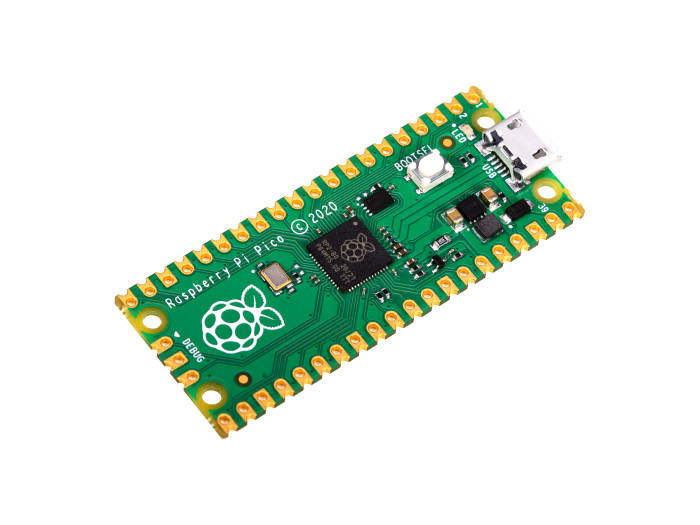
After we saw the launch of the Raspberry Pi 4 from the Raspberry Pi Foundation back in 2019, we are pleased to announce that the company has not rested on their oars as they have created their own microcontroller board called Raspberry Pi Pico, designed for not only the educationist or hobbyist but also for commercial products. The most interesting thing about this new board is that it is powered by an RP2040 dual-core Cortex-M0+ microcontroller designed by the foundation itself.
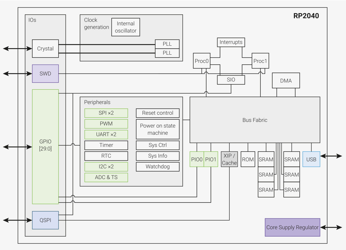
Let’s quickly talk about the RP2040 microcontroller. The name “RP2040” microcontroller is quite a unique one:
RP is short for Raspberry Pi,
2 – the number of cores
0 – the MCU core used (Cortex-M0+)
4 – floor(log2(ram/16k)) formula to calculate a number representing the SRAM
0 – floor(log2(non-volatile/16k)) formula for non-volatile storage capacity inside the chip.
The Raspberry Pi Foundation probably decided to create a custom MCU to prevent people from copying the hardware too easily and using their software. It could also be that they wanted to sell the RP2040 microcontroller to makers who are looking to design their own boards/projects with it because from updates being received, third party RP2040 boards have been announced by Arduino, Sparkfun, Adafruit, and Pimoroni already.
Now, to the Raspberry Pi Pico board itself. As we mentioned earlier, the Raspberry Pi Pico is based on the RP2040 microcontroller. It is a low-cost, high-performance microcontroller board with 2x ARM Cortex-M0+ cores run up to 133MHz, 256KB RAM, 30 GPIO pins, 2MB of onboard QSPI Flash memory for code and data storage, and a broad range of interfacing options. The only downside to this board is that the pins support only 3.3V, and there’s no 5V tolerance.
Raspberry Pi Pico Specifications:
Raspberry Pi RP2040 dual-core Cortex-M0+ MCU @ 48 MHz (maximum of 133 MHz) with:
264 kB of embedded SRAM in 6 banks
30x multifunction GPIO
6x dedicated IO for SPI Flash
Dedicated hardware for commonly used peripherals
Programmable IO for extended peripheral support
4 channel ADC with an internal temperature sensor, 0.5 MSa/s, 12-bit conversion
USB 1.1 Host/Device
SWD Debug interface
Package: QFN56 7x7mm
2MB QSPI flash
1x Micro USB 1.1 port (for power and programming)
2x 20-pin 2.54mm pitch header and castellated holes with 26x GPIOs, 3x 12-bit ADC, 2x UART, 2x I2C, 2x SPI, 16x PWM and 2x programmable high-speed I/O
3.3V I/O voltage
12-bit temperature sensor
3-pin Arm SWD port
BOOTSEL button
User LED
1x Timer with 4x alarms
RTC
5V via Micro USB port or 2V – 5V DC via VSYS pin
Dimensions: 51 mm x 21mm
The board doesn’t come with headers so you might have to solder them yourself or better still, buy the version with soldered headers.
Software support for the board is MicroPython and C/C++ programming with the command line or Visual Studio Code. Both the MicroPython and C/C++ SDK as well as hardware and software details are all available on the company’s Github. You’ll also find a “Get Started with MicroPython on Raspberry Pi Pico” manual provided by the company to help younger makers in their development journey.
Raspberry Pi Pico is currently selling for $4 without shipping. You can also choose to buy the version of the board with pre-soldered headers or the Basic kit that has a Pico board or the one that doesn’t. All versions of the board are available on RS Components, Cytron (ASEAN only), and Seeed Studio.
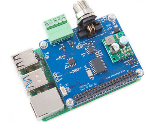
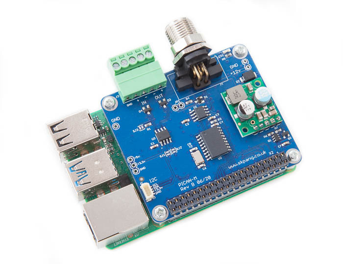
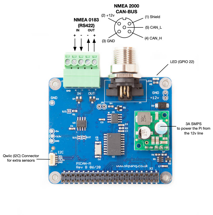
If you ever worked with a GPS location module in close proximity with the hardware, you might have an idea about the direction we are taking today, as you had to deal with NMEA strings. NMEA 2000 (or NMEA2K or even N2K) is something among those lines but emphasizes a bit more on the hardware than the former. It intends to be a plug-and-play protocol to connect devices inside marine vehicles, including sensors and display units. Electrically, it is compatible with the CAN protocol. Typical data exchanges within the NMEA 2000 protocol include position, GPS status, steering commands with autopilots, wind sensor data, among other important variables in the aquatic environment. Now that you have a vague idea of what it is, let us introduce you to an interesting HAT for the Raspberry Pi, the PICAN-M.
The PICAN-M is a Raspberry Pi HAT for location, which can be connected through NMEA 2000 or NMEA 0813. Along with the expected location functionalities, it provides you with a 3 A switch-mode PSU, so that you can power both the HAT and the Raspberry Pi from an on-board 12 V power source. Now, if you know anything about the Raspberry Pi hardware, your first question (like mine) is going to be: “how do I communicate with the HAT?”, because the communication on the Raspberry Pi is limited to UART, I2C, and SPI. There is no CAN. The easy answer is they added a CAN controller to the HAT (more specifically, the MCP2515 part) which communicates via SPI, so all you need is the CAN utils package and you are good to go. But you are not limited there, the NMEA 0183 allows communication via UART. It requires some extra effort, but if your application requirements leave you with no choice, you can still use it.
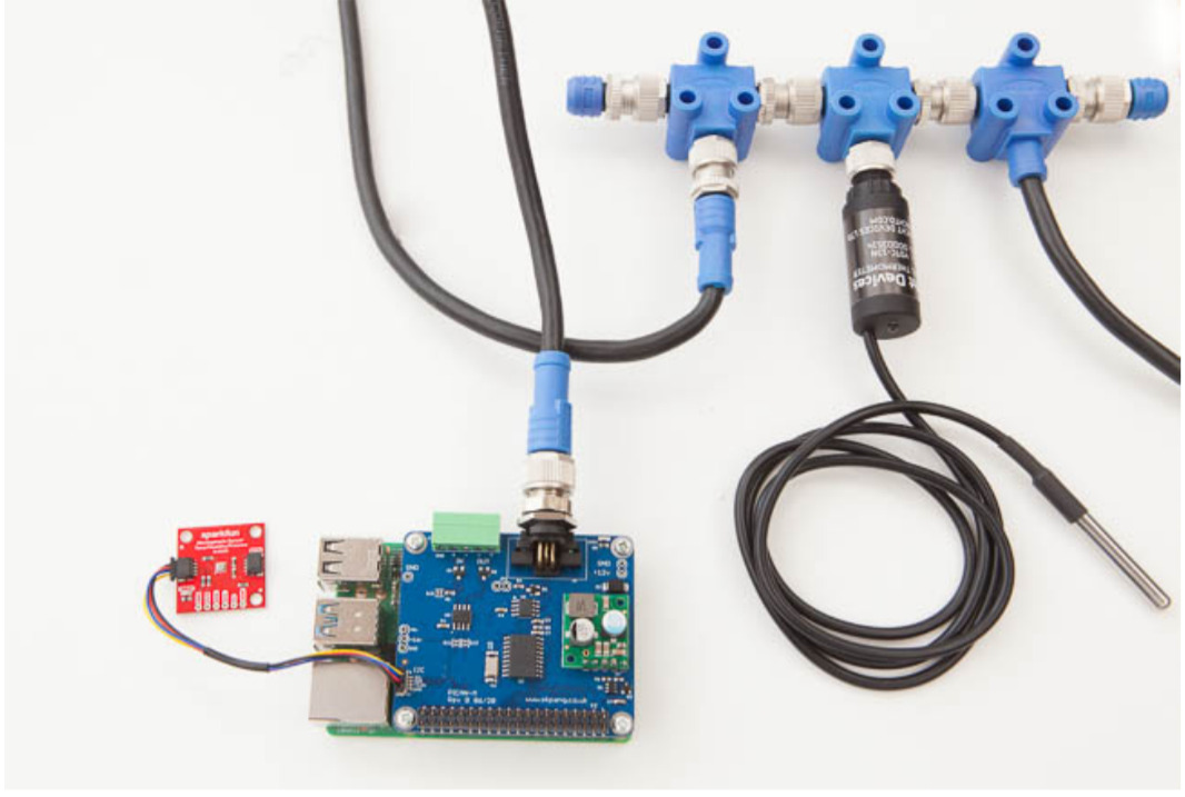
The PICAN-M all plugged in through CAN
Let us take a look at its specifications:
CAN bus connection via Micro-C connector
SocketCAN driver (appears as can0 to application)
NMEA 0183 (RS422) connection via 5-way screw terminal (appears as ttyS0 to application)
Qwiic (I2C) connector for extra sensors
3A Switch Mode Power Supply
Compatible with OpenCPN, OpenPlotter, SignalK, and CANBoat
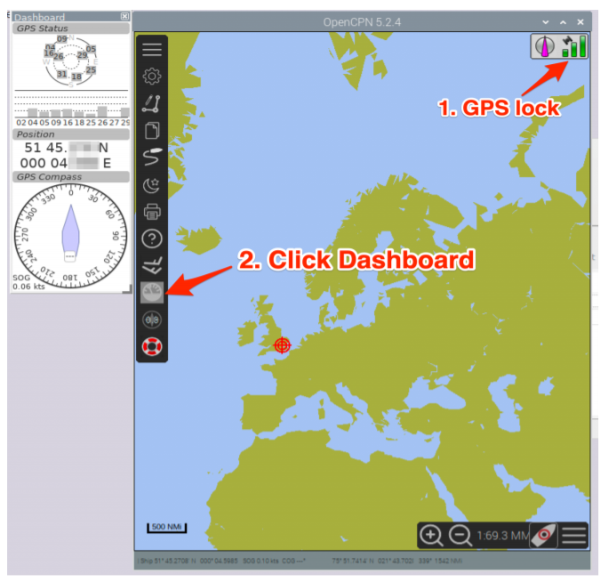
Now, we will take a look at the module in action. Of course, we will not go crazy and drive a boat. Firstly, we cannot, lockdown. Then, we have no module or boat license (or boat). So, we dove through its manual. It is not a bad experience, does not give you nausea from the sea and the documentation is actually pretty good. The image you are seeing is of the OpenCPN. There are more options, and the module only shines further if you put the I2C port to good use (by plugging a barometric pressure, humidity, and temperature sensor, like the BME280, from SparkFun). Lastly, the pricing of $98.85 is acceptable, considering the functionalities it provides you with.
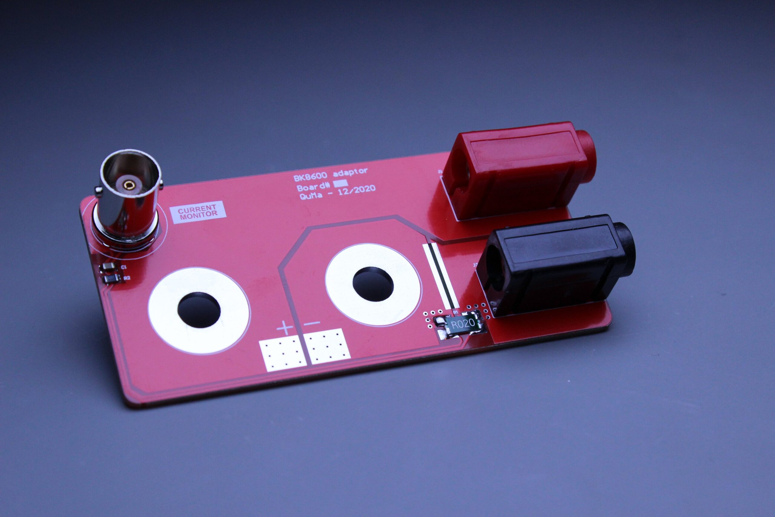
This product is a multi-purpose DC load terminal to banana cable adaptor. It includes solder pads for direct soldering of harnesses to the DC load output (convenient to add voltage sensing wires or wires from a power supply for battery emulation). Additionally, it has a fully integrated low-side shunt current sense circuit, locally filtered and outputted on a BNC connector. This allows viewing of the current waveform directly on your scope with extremely low noise.
This product is ideal for anyone that works with fast load or current transients and would like to observe those on an oscilloscope.
Options
This product can be sold in two options:
[Adaptor only] The adaptor board is shipped only with banana connector mounted. The board can be used out of the box as a DC load terminal to banana cable adaptor and solder pads. The current monitor circuit (BNC connector, shunt resistor and low pass filter) are left unmounted. The buyer is free to mount his own BNC connector (J3: 5-1634503-1) and preferred shunt resistor (R1: LVK24) and low pass (C1, R2: 0805 size).
[Adaptor with current monitor] The adaptor board is shipped fully mounted with a 20mOhm/1W shunt resistor, 16kHz low-pass filter (1kOhm, 10nF) and the BNC connector installed. This corresponds to 20mV/A rated for 7A. This is the ideal option if you would like to observe load or current transients on an oscilloscope.
You can buy the adaptor on Tindie for 5.00 + shipping.
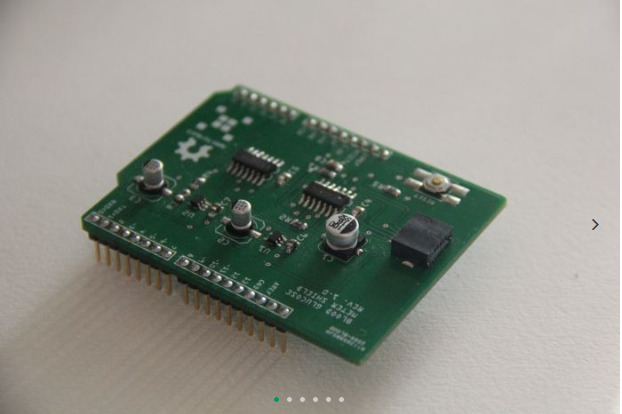
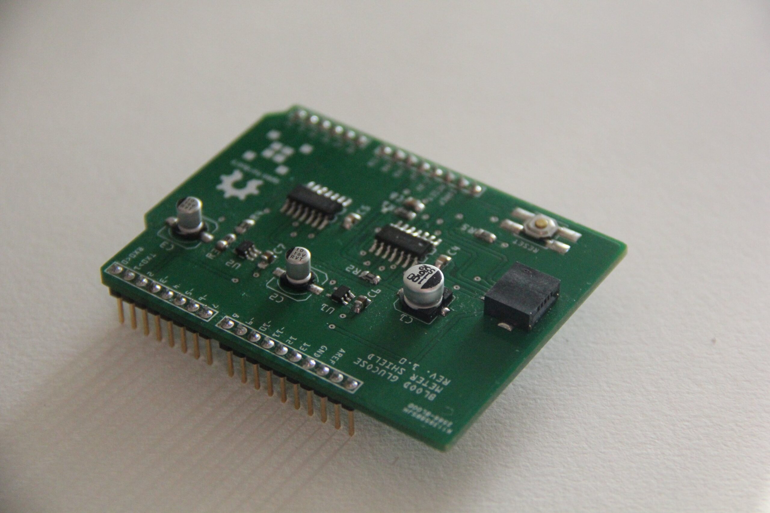
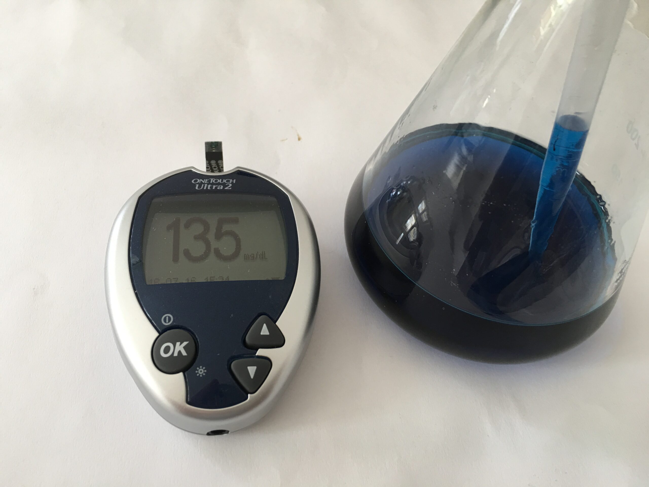
Diabetes is a serious disease that affects millions of people around the world today. Diabetes affects the body’s ability to produce insulin, a hormone that enables the body to turn glucose into sugar which has resulted to a large number of deaths, an estimate of 1.6 million deaths yearly caused by the illness. This is why it is very important such illness should be diagnosed early for effective management, because if left untreated, it can lead to heart disease, kidney damage, nerve damage, and stroke. This has led Markus Bindhammer to embark on an open source blood glucose meter shield project. This project competed and won an award at the Assistive Technologies category of the 2016 Hackaday prize. The glucose meter plays a large part in effective control, as this provide patients with the ability to monitor blood glucose levels from the comfort of their homes. You can obtain the glucose meter at your local val pharmacy. It is easy to use, the patient insert one of the disposable test strips into the meter, prick their finger, load a droplet of blood into the test strip, wait a few seconds and get an instant reading of the current blood glucose level. .
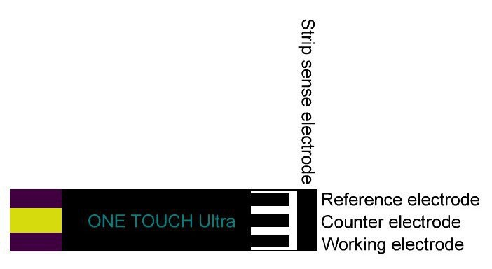
Designed by M.Bindhammar, the aim of the project is to measure blood glucose level using electrochemical test strips. The glucose meter shield functions by receiving blood sample through a one touch Ultra test strip and output the results on the Arduino IDE serial monitor window. The test strip features three electrodes which are printed into the test strips. They include: a reference electrode, a counter electrode and a working electrode. A fixed voltage is supplied, and the resulting current after the blood is added is monitored. The response it give is then measured to the glucose concentration through calibration. You should note that some models requires a user to manually enter a code found on a chip that comes with the test strip since test strips can vary from batch to batch. This code enables the meter to be calibrated to a particular batch of test strips. The brand of test strips used is the ONE-TOUCH which has standardized test strips around a single code number so for a particular set there is no need to change code in their older meters and some of their newer meters.
The electrodes of the strips are coated enabling an enzymatic chemical reaction to take place on the surface of the electrode, and this reaction determines the resulting current. We find little details about electrochemistry, and details available can be quite complex. Also some companies do not release detailed data about their particular test strips operation. But some devices functions by watching the current after a short initial transient (the current will level out to some degree) and then report the current after a fixed time. Others examine the total amount of a reaction that has occurred and thus integrates the current with regard to time in order to obtain the total amount of chemical reaction that has occurred. However, the Open source Arduino blood glucose meter functions by making two measurements to determinate which relates more strongly to the glucose level: one is the current after a fixed time and the other is the total integrated current.
Markus Bindhammer owns all of the design’s intellectual property rights and is responsible for end-user support. About production and sales, Seeed says
“If the Groupbuy meets the target quantity within the allotted timeframe, the Groupbuy is deemed a success, and Seeed will initiate the production and delivery of the goods after payment is made.If the Groupbuy fails Seeed will refund all buyers within 10 working days.”
You can find more information about glucose meter shield on Seeedstudio, and Hackaday.
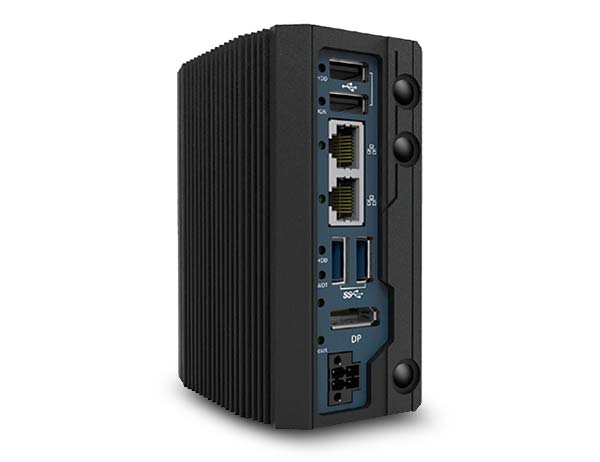
Neousys Technology, an industry-leading provider of rugged embedded systems, today announced its new extreme ultra-compact fanless embedded computer, the POC-40. Featuring Intel’s latest Atom processor and a 2.5-inch SSD-like dimension measuring just 50 mm (W) x 87 mm (D) x 112 mm (H), it is ideal for installation into limited spaces and is designed for applications such as factory data collection, rugged edge computing and mobile gateway.
POC-40 features Intel’s 10nm process technology, the new-generation Elkhart Lake Atom® x6211E dual-core processor offers 1.7x the single thread and 1.5x multi-thread performance over the previous Gemini Lake Atom CPUs. In addition to the performance boost, the system is also smaller than the previous generation. To put things in perspective, when compared to the Neousys POC-200 series, POC-40 has the 2x processing power at almost only half the size.
With its DIN-rail mountable design, all of POC-40’s rich high-speed I/Os can be easily accessed. They include two Gigabit Ethernet, four USB (2.0/ 3.1 Gen1), four COM and optional isolated digital I/Os for industrial communication and control. As for internal expansion, it has an M.2 B key socket and an M.2 E key socket for 5G/ 4G/ WiFi 6/ WiFi 5 modules to provide wide-area coverage and real-time data transmission for industrial and mobile gateway applications.
Features
Intel® Elkhart Lake Atom® x6211E dual-core processor
49 x 89 x 112 mm extremely compact form factor
Rugged -25°C to 70°C fanless wide-temperature operation
Two GigE ports, two USB 3.1 Gen1 ports and two USB2.0 ports
M.2 2280 M key SATA storage interface
One M.2 B key socket supporting 5G/ 4G 3042/ 3052 modules
One M.2 E key socket for WiFi 5/ WiFi 6 modules
One COM port with RS-232/ 422/ 485 modes and three RS-232 COM ports
As a fanless industrial-grade computer, POC-40 supports 8V DC to 35V DC wide-voltage operation, -25°C to 70°C wide-temperature operations, and two installation methods, it can be DIN-rail or wall-mounted. On top of all the jammed-packed features in such a small enclosure, the POC-40 is United States Military Standard (MIL-STD-810G, Method 514.6) certified to withstand vibration.
“POC-40 is an x86-based computer platform enclosed within an extremely compact fanless design. Comparing to a ARM-based gateway, it provides significantly more computing power in similar dimensions. With rich I/Os and the ability to support the latest wireless communication modules, POC-40 is fundamentally sound, easy to implement and can be deployed into industrial environments for edge/ fog computing or decentralized data collection and processing”
said Ariel Chen, product manager of Neousys Technology.
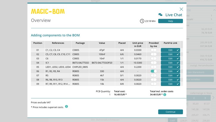
MAGIC-BOM® is the latest feature in the PCB-POOL® configurator from the prototype specialist and PCB manufacturer Beta LAYOUT.
MAGIC-BOM® creates your Bill of Material (BOM) for PCB assembly as if by Magic;
How does it work ?
You simply drag your PCB layout file into the ‘drag & drop’ field.
The MAGIC-BOM Tool first checks whether the components are available in Beta LAYOUT’s component stock inventory, which automatically saves you time as well as reducing component and shipping costs.
If your component is not available, Magic BOM will suggest suitable components from various distributors, which you then only have to select.
As soon as all components have been selected and the parts list has been completely filled out, the price for components, assembly service and PCB manufacture is displayed instantly.
After ordering, you will receive the parts list (BOM) in excel format for documentation purposes.
The benefits for you:
Cheaper and faster assembly through our own stocked components.
Faster creation of your parts list – you only confirm the correct components.
young asian man using apps in smartphone and smartwatch to track fitness data during exercise
Author: Matthew Leonard
Introduction
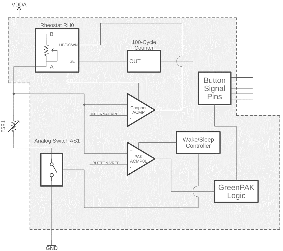
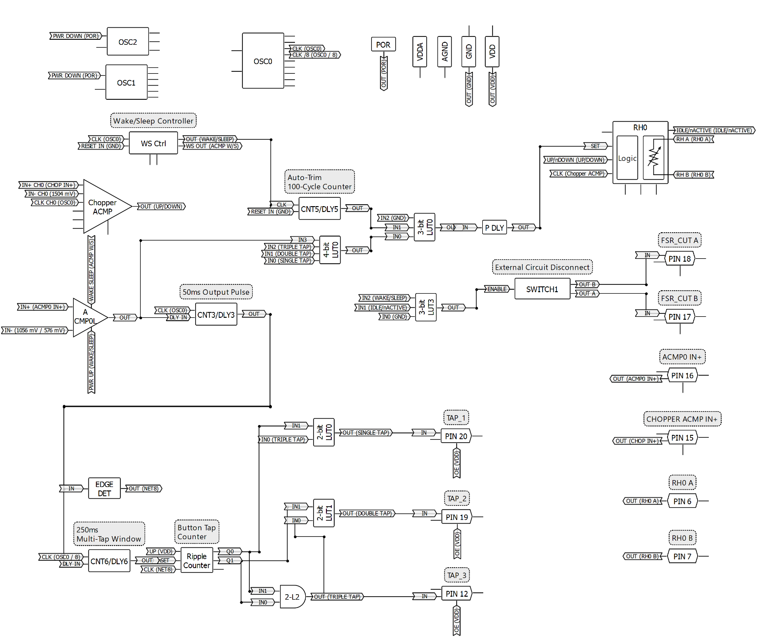
A common requirement for devices that must be sealed from environmental exposure is to replace all metal contact style push-buttons with functional replacements that do not have those weather-sealing difficulties. This article describes one such way of creating a contact button replacement using a Force-Sensitive Resistor (FSR) in conjunction with an SLG47004V.
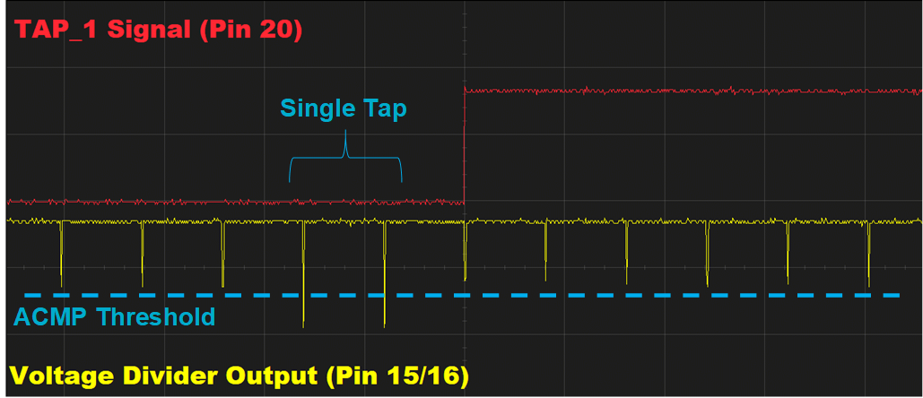
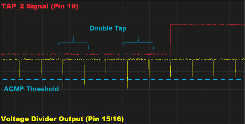
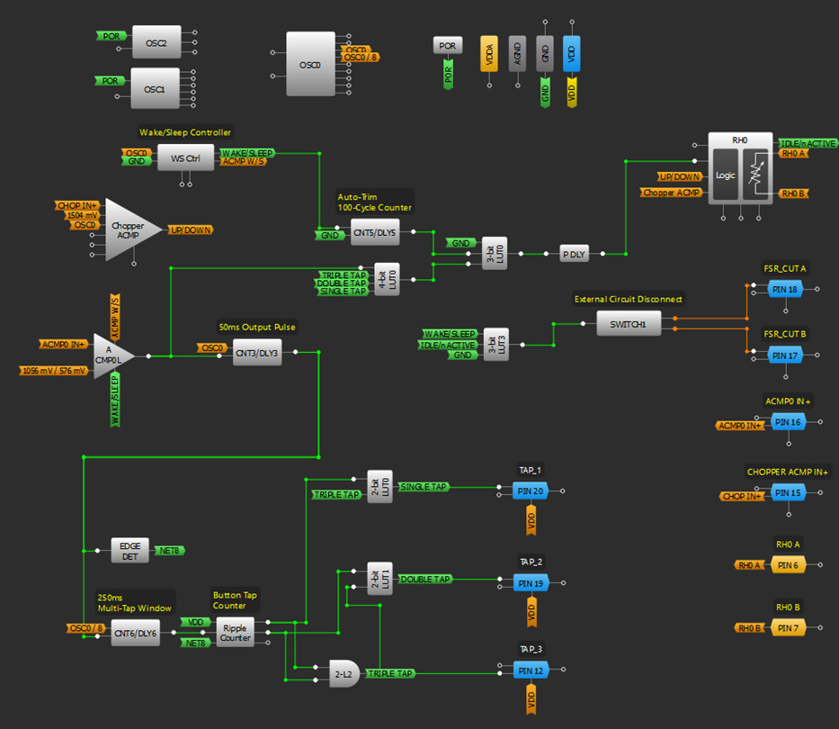
The design highlighted above is intended for use as a functional replacement for a metal contact style push-button while featuring ultra-low power consumption. Using an external force-sensitive resistor in series with one of the IC’s internal rheostat modules, a resistor divider network is created which is subsequently sampled by one of the SLG47004V’s internal low-power ACMPs. This ACMP determines the state of the button based on the voltage present at the divider output. Once the internal low-power ACMP determines that the button has been pressed, internal GreenPAK logic processes the button press signal to determine whether a single, double, or triple-tap has occurred, and outputs these signals to dedicated pins.
Since the force-sensitive resistor present in this design is highly susceptible to variation in resistance due to temperature changes, often as severe as +/-15% at extreme high/low temps, a constant “no-press” reference voltage must be maintained throughout a wide range of temperatures. This constant reference voltage is achieved using the circuit’s auto-trim functionality, which periodically samples the divider output voltage and adjusts the SLG47004V’s internal rheostat resistance, allowing the divider output to return to the specified “no-press” reference voltage. This auto-trim functionality not only allows for accurate operation over a wide range of temperatures, but it also allows the design to accommodate for sensor-to-sensor variations as well as variations in the overall system voltage level.
To attain ultra-low current consumption, the ACMP and external resistor divider network are controlled by the integrated circuit’s wake/sleep controller. This wake/sleep controller keeps the ACMP in sleep mode via matrix signal, and the resistor divider circuit in an open state via one of the IC’s internal analog switches, which is placed on the low side of the divider. The Chopper ACMP, which is responsible for the IC’s auto-trim functionality, is also indirectly controlled by the wake/sleep controller using an intermediate counter that triggers an auto-trim cycle once every 100 normal wake/sleep cycles.
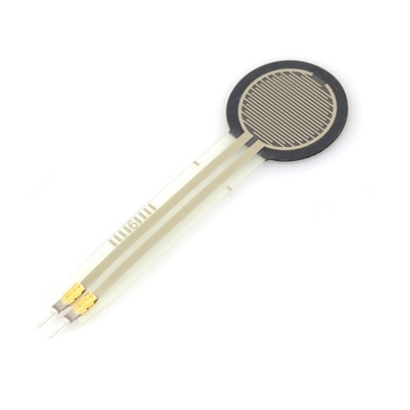
Figure 4: A Standard FSR
Mechanical Pre-Loading of the FSR Sensor (Required)
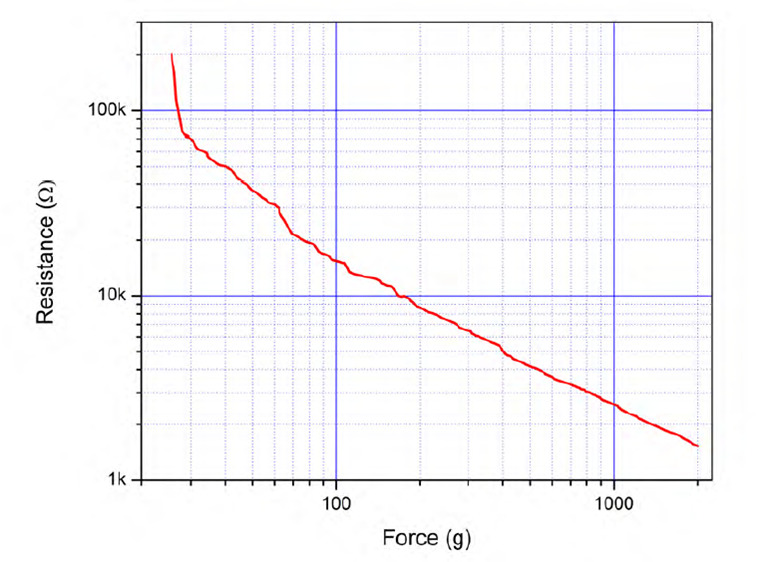
To properly trim the voltage divider circuit to the desired output voltage using the circuit’s digital rheostats, a small, consistent amount of force must be permanently applied to the FSR sensor before trimming can occur. This is due to the FSR’s very high no-load resistance, which measured over 100 MΩ in this test and is shown by the graph below, being far too large for the IC’s digital rheostats to compensate for. Pre-loading the FSR with a small mass will lower its base “un-pressed” resistance into a range that will allow the SLG47004V’s digital rheostats to properly trim the voltage divider. It is worth noting that this process does not require a specific force value to be applied, so long as the force applied satisfies two requirements:
The applied force creates a large enough resistance drop within the FSR to allow for proper trimming of the voltage divider.
The applied force remains constant throughout the lifespan of the application.
Figure 5: FSR Resistance vs Force Applied
Auto-Trim Overview
To adequately implement an FSR sensor as a button replacement, considerations must be made for its rather large temperature dependency. Ideally, the no-press output voltage of the system would remain constant over temperature, allowing for a detecting ACMP to be tuned to detect button presses at all temperatures. Since the FSR’s resistance does not remain constant over temperature, the SLG47004V becomes responsible for maintaining this output voltage.
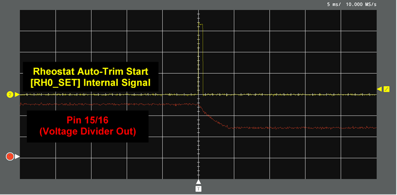
In this article, the circuit’s rheostats are used for their auto-trim capabilities, which adjust their resistance to match an internally generated reference voltage. This auto-trim process occurs whenever a high signal is provided to the rheostat’s “SET” pin. When this signal is brought high, either externally or via internal logic, the auto-trim process begins. A waveform of this process is provided at the end of this section, which shows the “SET” signal being brought high, and the voltage divider output voltage changing to match the internally set reference voltage which, in this waveform, is 1.5 V.
This auto-trim process, if implemented to occur periodically during the runtime of the device, will provide a very high level of consistency in the voltage divider’s output voltage. This, in turn, allows for one of the IC’s internal ACMPs to be used to detect press signals on the FSR and can be adjusted to detect presses at all temperatures within the range of the device.
Two points of functionality were measured to determine the success of the design. First, the design had to function as a button replacement, triggering the appropriate output signals in response to certain button-press sequences. Second, the device had to consume as little power as possible. Given that this type of design may be valued for its use in wearable technology, a maximum quiescent current of 10 uA was imposed as a design restriction.
Button-Press Functionality
Waveform captures of various operation conditions of the FSR button setup can be found below with accompanying descriptions and labels. VDDA was, in this test, set to 3.3 V and the FSR was given a small amount of mechanical pre-loading. Additionally, the auto-trim reference voltage was set to 1.5 V, and the rheostat’s “SET” signal was configured to be brought high by an internal counter block every 100 ACMP sample-cycles.
Figure 7: Single-Press Signal Vertical 1 V/div Horizontal 50 ms/div
Figure 8: Double-Press Signal Vertical 1 V/div Horizontal 50 ms/div
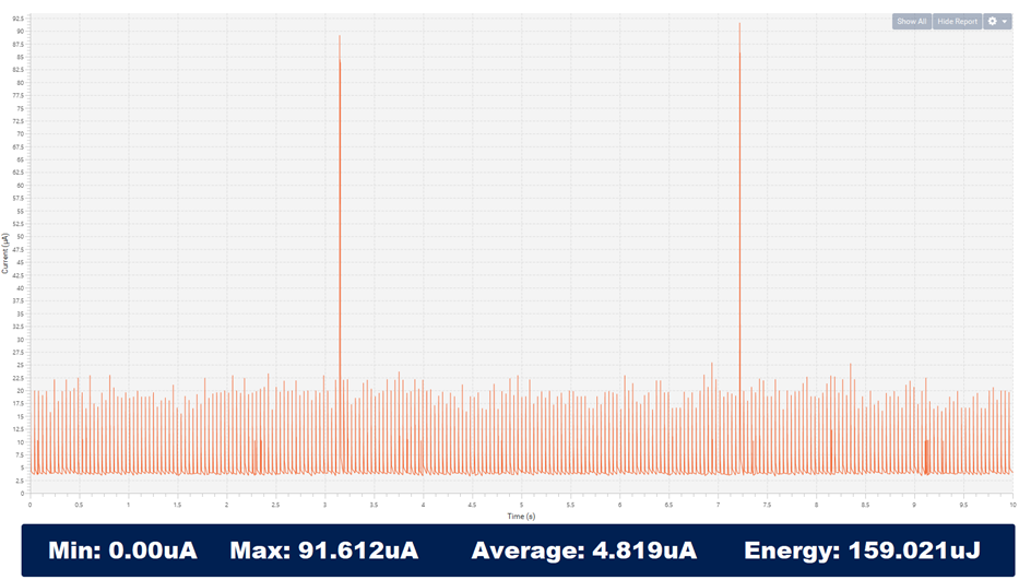
Current Consumption
Testing of quiescent current took place primarily at a sample rate of 25 Hz, as this is the lowest sample rate which seemed to provide an adequately responsive button design. A DC power monitor was used to capture the average Iq of the device, with external circuity included, over ten seconds, and the sample rate of said power monitor was set to 50 kHz for these tests. Below is the capture window of said DC power monitor:
Figure 9: Current Consumption Graph
The two spikes present in the capture represent the auto-trim windows of the design, which are responsible for modifying the circuit’s internal rheostat value to allow the voltage divider in the above schematic to match a reference voltage. Since the device has already been properly auto-trimmed at this point, the SLG47004V’s internal chopper ACMP responsible for the auto-trim functionality is immediately turned off, thus resulting in a short spike. Each of the smaller spikes in the capture represents the circuit’s internal low-power ACMP being powered up to check if this reference voltage has dropped below a certain threshold, which would signal a button press has occurred.
The main testing parameter that prevents a higher level of precision when conducting this test is the fact that the force-sensitive resistor used in this design must be given a certain amount of mechanical “pre-loading” force for the resistance of the sensor to fall within a range that the circuit can effectively auto-trim. This sensor is very sensitive to not only the amount of force on the sensor but to the exact position of the force on said sensor. Since the sensor is too small for various reference weights to be used, the average active current measurements can be observed to fluctuate between 4 uA and 5 uA from test-to-test.
Conclusions
This design was tested at several sample rates, ranging from 10 Hz to 1 kHz. Of these sample rates, it was determined that to provide both adequate button performance and low power consumption, 25 Hz seemed to be the ideal ACMP sampling frequency. Under all tested conditions, however, the combination of SLG47004V and FSR proved to be a stable and well-performing button replacement solution.
This IC design was created in free GreenPAK Designer software. The complete design file can be found here.
WBG power semiconductor devices in silicon carbide and GaN technology provide design advantages that are allowing previously unimaginable application performance: low leakage current, significantly reduced power losses, higher power density, higher-frequency operation, and the ability to tolerate higher operating temperatures, all with a smaller device size than could be achieved for a silicon-only equivalent. Other features, of no lesser importance, are robustness and increased reliability, resulting in improved overall device life expectancy and increased operational stability.
Energy efficiency is now a strategic initiative in increasingly power-reliant industries such as data centers, electric vehicles, and the green grid. GaN-based devices hold the key to addressing a primary hurdle for the expansion of renewable energy.
From a power management standpoint, all power systems require a high level of integration to achieve the required portability. High energy efficiency is required for truly portable and therefore battery-operated systems. Lower power consumption maximizes device operating time without recharging or replacing the batteries.
GaN must operate safely and efficiently in a high-frequency ecosystem to fulfill its role in advancing the necessary revolution in fast charging, power conversion and energy storage. Integrating GaN FET, GaN analog, and GaN logic will yield a true GaN power IC.
The “AspenCore Guide to Gallium Nitride” is now available for purchase at eetimes.com/shop/
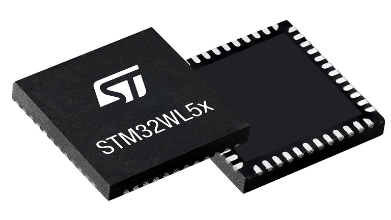
STMicroelectronics’ long-range wireless and ultra-low-power devices embed a powerful ultra-low-power LPWAN-compliant radio solution
STMicroelectronics’ STM32WLE5/E4xx long-range wireless and ultra-low-power devices embed a powerful ultra-low-power LPWAN-compliant radio solution, enabling the LoRa® (available in STM32WLx5xx only), (G)FSK, (G)MSK, and BPSK modulations. These MCUs are compatible with standardized or proprietary protocols such as LoRaWAN®, Sigfox, W-MBUS, and more (fully open wireless system on chip).
Features
Key features
Arm® Cortex®-M4 CPU up to 48 MHz
Up to 256 KB Flash and 64 KB SRAM
Sub-GHz radio – multi-modulations: LoRa, (G)FSK, (G)MSK, BPSK
Peripherals: 3 x I²C, 2 x USART, 1 x LP-UART, 2 x SP
Additional features
Radio
Frequency range: 150…960 MHz
Modulation: LoRa®, (G)FSK, (G)MSK, and BPSK
RX sensitivity:
-123 dBm for 2-FSK (at 1.2 Kbit/s)
-148 dBm for LoRa® (at 10.4 kHz, spreading factor 12)
Transmitter high output power, programmable up to +22 dBm
Transmitter low output power, programmable up to +15 dBm
Compliant with the following radio frequency regulations:
ETSI EN 300 220, EN 300 113, EN 301 166, FCC CFR 47 Part 15, 24, 90, 101, and the Japanese ARIB STD-T30, T-67, T-108
Compatible with standardized or proprietary protocols such as LoRaWAN®, Sigfox™, W-MBus, and more (fully open wireless system-on-chip)
Ultra-low-power platform
1.8…3.6 V power supply
-40…+105 °C temperature range
Shutdown mode: 31 nA (VDD = 3 V)
Standby (+ RTC) mode: 360 nA (VDD = 3 V)
Stop2 (+ RTC) mode: 1.07 µA (VDD = 3 V)
Active-mode MCU: < 72 µA/MHz (CoreMark®)
Active-mode RX: 4.82 mA
Active-mode TX: 15 mA at 10 dBm and 87 mA at 20 dBm (LoRa® 125 kHz) Core
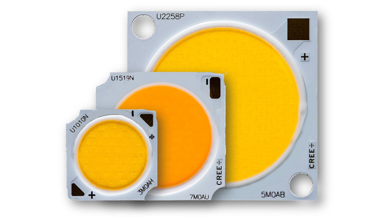
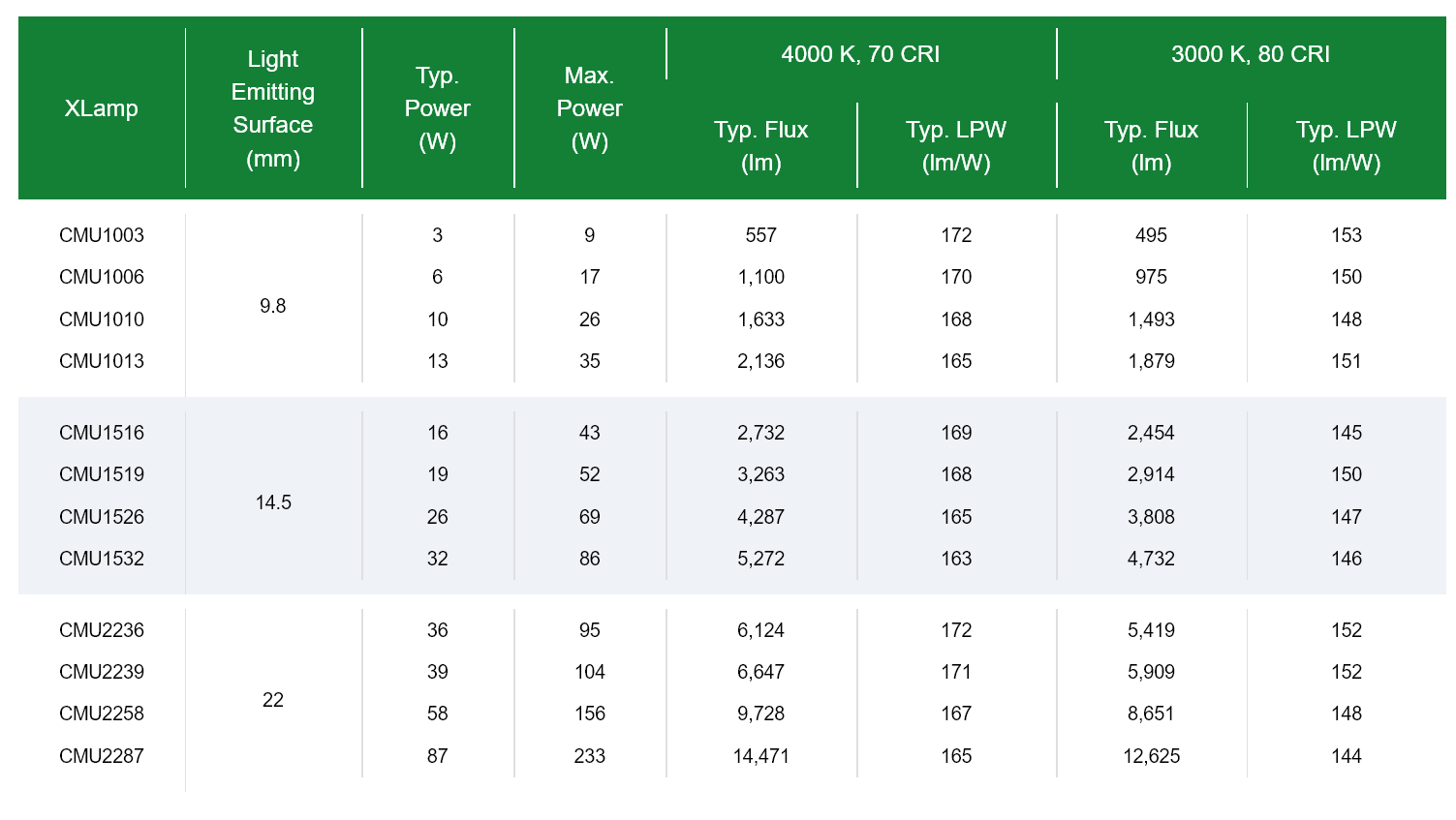
The new CMU family of COB LEDs is based on metal substrate as the previous CMT family compared to which it brings a 10% lumen per watt improvement. Not only CMU COBS deliver highest performance in the standard packages but they are available in various CRIs and CCTs including 2200K. Another differentiating feature reinforcing their cost attractiveness is their much higher max drive current (+30¨%) than currently available products from competition.
Key features
Industry-leading performance in commonly-available LES sizes
Delivers up to 10% higher LPW than previous generation CMT family
Optimized for outdoor & premium indoor lighting applications including track, spot and downlight