WADE-8212 mini-ITX embedded motherboard released

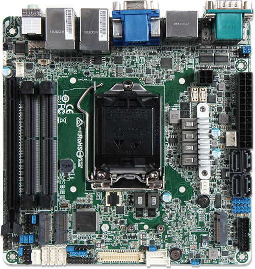
Portwell has announced WADE-8212, the latest addition to its family of Mini-ITX form factor embedded system boards. According to Brian Lai, Portwell’s product manager, the new WADE-8212 is designed to provide more powerful multi-tasking function and enhanced high-definition imaging capability with faster network (2.5Gb) connectivity.

Its rich I/Os and expansion support multiple peripheral devices in diverse applications such as industrial automation, robotic manufacturing, automated test equipment, semiconductor equipment, factory process control, automated guide vehicle (AGV), medical equipment, communications appliances, IoT gateway, smart transportation and much more.

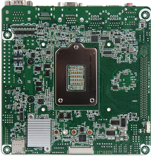
WADE-8212 supports the Intel Q470E chipset and the latest 10th Intel Core i9/i7/i5/i3/Pentium/Celeron processor platform (formerly Comet Lake S) up to ten cores/20 threads (35W-80W) in LGA1200 socket.

Additional features:

  • Dual-channel DDR4 2400/2666/2933MHz Non-ECC SDRAM on two SO-DIMM sockets up to 64 GB.
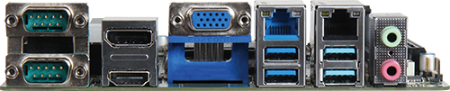
  • One and 2.5 Gigabit Ethernet (Intel I219LM and I225LM).
  • Five COM ports (Two are BIOS configurable).
  • Six USB 3.2 Gen 1 and four USB 2.0.
  • Four SATA III ports, GPIO and Audio Jack.

Rich expansion interface includes:

  • One PCIe Gen 3 x16, 1x M.2 key E 2230 for wireless modules (Bluetooth/Wi-Fi).
  • One M.2. key M 2242/2260/2280 for SSD.
  • One M.2 key B 3042 and SIM card socket for 4G/5G.
  • Triple display includes 1x DP 1.2 (4K resolution).
  • One HDMI 2.0a (4K resolution).
  • One VGA (resolution up to 1920×1200) on rear.
  • One LVDS (resolution up to 1920×1200) connector on board.
  • ATX power; and onboard TPM 2.0 for security.

“The newly-designed WADE-8212 features the latest Intel 10th Generation Core processors,” said Lai. “This means it now offers up to 20% more cores than previous generation processors, up to 31 percent better performance on multi-tasking compute-intensive applications, and as much as 11 percent improved performance on single-task compute-intensive applications.

“But the benefits don’t stop there. It features MOSFET Heatsink to dissipate heat more efficiently and is suitable for fanless systems. To enhance serviceability, it has the option to use rechargeable CMOS battery for longer CMOS data retention. A compact PCIe card guide is designed to make easier installation and prevention of damage. Its 2.5 Gigabit LAN support (Intel I225LM) can boost networking performance up to 2.5 times faster than a traditional 1 Gigabit LAN, so the user benefits from faster file transfers and smoother video streaming while retaining high quality.

“What’s more, the improved WADE-8212 boasts a wide range of I/O and rich expansion, including 1x PCI Express x16 and multiple M.2 slots for wireless connectivity, storage and increased functionality in a wide range of applications. In addition, our customers not only benefit from the most up-to-date technology and features, but they also gain peace of mind from the long product life span (15+ years) inherent with every Portwell product.”

more information: https://portwell.com/products/detail.php?CUSTCHAR1=WADE-8212

EDLC Series Electric Double Layer Capacitors/Supercapacitors rated at 500mF

TDK’s electric double layer capacitors are small in size with a low profile

TDK’s electric double layer capacitor (EDLC) is a charge storage device that offers higher capacitance and higher energy density than an electrolytic capacitor. The EDLC stores charge using an electric double layer formed by ions adhering to the surface of an activated carbon electrode and can be charged in a matter of seconds (see Figure 1). The EDLC series products are constructed with the latest material and processing technologies and feature high capacitance and low resistance. Because a metal foil laminated film is used for packaging, EDLC series products are small in size with a low profile, allowing for space-saving designs. These components are excellent for a wide range of applications, including memory backup in electronic devices, battery load leveling in mobile devices, energy harvesting, and more.

Figure 1: Charging process for an electric double layer capacitor
Features
  • High capacitance and low impedance
  • Small size, low-profile design
  • Operating temperature range from -30°C to +70°C
Applications
  • Battery assistance
  • Storage element of energy harvesting
  • Strong LED flash
  • Backup application for instantaneous power failures

more information: https://product.tdk.com/info/en/products/capacitor/edlc/edlc/index.html

B58621V Medical Sensors make measurements in the flow lines

EPCOS’ medical sensors precise measurements in the flow lines allow flow rates to be calculated accurately in ventilator equipment

TDK Corporation’s B58621V range of highly accurate differential pressure sensors, are designed as printed circuit boards. The sensors are designed for measurement ranges of 16 mbar full-scale (FS), 100 mbar FS and 7 bar FS, with an absolute accuracy of up to ±1% FS at temperatures from -20°C to +70°C.

The footprint of 24 mm x 26 mm accommodates pressure ports and inlets (allowing for simple screw fitting and easy maintenance) as well as two plug connectors for easy implementation of daisy chain systems. The integrated SPI enables easy integration into various digital applications. The sensors are EN ISO 13485-certified for use in medical devices. Precise pressure loss measurements in the flow lines allow flow rates to be calculated accurately in ventilator equipment, and they are particularly well suited for mobile ventilators due to their extremely low profile of only 6 mm. The sensors are also suitable for monitoring filters and gas admixtures.

  • Extremely low profile: 6 mm height
  • Measurement ranges from 16 mbar to 7 bar
  • Highly accurate up to ±1% FS
  • EN ISO 13485 certified
  • Stationary and mobile ventilators
  • Filter and gas admixtures monitoring

more information: https://product.tdk.com/en/search/sensor/pressure/pressure-transmitter/info?part_no=B58621V2712B537

The VCNL36825T integrates a proximity sensor (PS), and a VCSEL into one small package

The VCNL36825T integrates a proximity sensor (PS), and a VCSEL into one small package. It incorporates photodiodes, amplifiers, and analog to digital converting circuits into a single chip by CMOS process. PS programmable interrupt features of individual high and low thresholds offers the best utilization of resource and power saving on the microcontroller.

Key features

  • Integrated modules: VCSEL, proximity sensor (PS), and signal conditioning IC
  • Low power consumption I2C (SMBus compatible interface)
  • 1.6 mm single hole opening design
  • Temperature compensation: -40 °C to +85 °C

Additional features

  • Package type: surface-mount
  • Dimensions (L x W x H in mm): 2.0 x 1.25 x 0.5
  • Integrated modules:
    • Vertical-cavity surface-emitting laser (VCSEL)
    • Proximity sensor (PS)
    • Signal conditioning IC
  • Interrupt function
  • 1.6 mm single hole opening design
  • Supply voltage range VDD: 2.64 V to 3.6 V
  • Low power consumption I2C (SMBus compatible interface)
  • Interface: I2C bus
  • Temperature compensation: -40 to +85 °C
  • Floor life: 168 h, MSL 3, according to J-STD-020
  • Proximity functions:
    • Immunity to red glow (940 nm IRED)
    • Programmable IVCSEL sink current
    • Intelligent cancellation to reduce cross-talk phenomenon
    • Smart persistence scheme to reduce PS response time
    • Low power consumption mode
    • Sunlight cancellation up to 100 klx
  • Interrupt:
    • Programmable interrupt function for PS with upper and lower thresholds
    • Adjustable persistence to prevent false triggers for PS

more information: https://www.vishay.com/optical-sensors/list/product-80235/tab/quality/

VEML3235SL is an advanced ambient light sensor with an I2C protocol interface

VEML3235SL is an advanced ambient light sensor with an I2C protocol interface and designed using the CMOS process

VEML3235SL is an advanced ambient light sensor with an I2C protocol interface and designed using the CMOS process. The VEML3235SL incorporates a photodiode, amplifiers, and analog circuits in a single chip. The best spectral sensitivity is used to obtain a response close to the response of a real human eye. It has excellent temperature compensation and a robust refresh rate setting that does not need an external RC low pass filter. Software shutdown mode is provided, which reduces power consumption to be less than 1 μA. The sensor’s operating voltage ranges from 2.6 to 3.6 V and can detect a wide range of ambient light intensities.

Key features

  • Supply voltage range VDD: 2.6 V to 3.6 V
  • Communication via I2C interface
  • I2C bus H-level range: 1.7 V to 3.6 V
  • Floor life: 168 h, MSL 3, according to J-STD-020

Additional features

  • Package type: surface-mount
  • Dimensions (L x W x H in mm): 2.95 x 1.5 x 1.5
  • Integrated modules: ambient light sensor (ALS)
  • Supply voltage range VDD: 2.6 V to 3.6 V
  • Communication via the I2C interface
  • I2C bus H-level range: 1.7 V to 3.6 V
  • Floor life: 168 h, MSL 3, according to J-STD-020
  • Low stand by current consumption: typ. 1 μA
  • Material categorization: for definitions of compliance please see www.vishay.com/doc?99912
  • PLICATIONS
  • Handheld device
  • Notebook
  • Consumer device
  • Industrial and medical application
  • Computing, and industrial devices and displays
  • Ambient light function:
    • High ALS sensitivity with the minimum detectable intensity of 0.0021 lux/cnt supports a low transmittance lens design
    • Excellent temperature compensation
    • High dynamic detection resolution
    • Software shutdown mode control

more information: https://www.vishay.com/optical-sensors/list/product-80011/

T3AWG3252 Multifunctional 16-bit Arbitrary/Function Generator With Innovative Architecture and Digital Pattern Generation

The T3AWG3252’s analog/digital synchronized output represents a valuable tool to simulate, troubleshoot, or validate digital designs.  

Saelig Company, Inc. has introduced the Teledyne LeCroy T3AWG3252 Multifunctional 16-bit Arbitrary/Function Generators that are designed with an innovative architecture that features synchronized analog signal and digital pattern generation. This multifunction 250MHz arbitrary/sweep/function generator combines multiple functions in a single instrument, including a two-channel function and arbitrary waveform generator with an eight-channel digital pattern generator. These three different functionalities are based on an advanced Direct Digital Synthesis (DDS) technology which allows glitch-free on-the-fly changes of all parameters while preserving the selected waveform shapes. All controls and settings are available with touch/swipe gestures on the color LCD. This makes it east to change channels, select the carrier, access the modulation parameters, access the waveform gallery to quickly import a chosen signal, or use the virtual numeric keyboard to change parameter values.

The variable clock, true-arbitrary technology of the Arbitrary Waveform (AWG) / Digital Pattern Generator lets the user create complex signals of synchronized analog waveforms as well as digital patterns. Users can create signals in a sequence, or apply loops, jumps, and conditional branches. The analog/digital synchronized outputs represent a valuable tool to simulate, troubleshoot, or validate digital designs. Users can use the waveform sequencer to generate quite complex or very long signals with multiple waveform shapes. The AWG mode uses a variable or synchronized sample rate ‘True-Arb’ technology to suit applications requiring extremely high signal fidelity. The platform’s deep memory enables the capability to store numerous long waveforms.

  • 16-bit vertical resolution
  • 1GSa/s sample rate
  • 128Mpts (up to 1Gpts option) memory on each channel
  • 16,384 waveform entries in the sequencer
  • Output impedance 50 Ohm and 5 Ohm  selectable
  • + / – 24V output

Application tasks for which this test instrument is especially suited include the Distortion Test for Automotive Ethernet 100Base-T1 and 1000-Base-T1Power and the Semiconductor Dynamic Behavior Test, made easier with the instrument’s versatile double-pulse test capability. Among the compliance tests specified for the Automotive Ethernet standard none is more complex to set up than the transmitter distortion test. Using the T3AWG3252, as well as a Teledyne LeCroy oscilloscope and the QualiPHY Compliance Manager, testing is greatly simplified. The T3AWG3252’s excellent Harmonic Distortion performance, combined with the output voltage amplitude range and the precise tuning of the delay and phase of the differential signal pairs, makes the T3AWG3252 a perfect tool for emulating the disturber signal to assist in avoiding pitfalls encountered during the execution of the test.  The T3AWG3252 can also quickly determine the dynamic behavior of power devices. The standard feature Double Pulse function required for testing MOSFETs and IGBTs is made simpler because the two pulses can have a different amplitudes, rise-times, fall-times, and widths.

The Teledyne LeCroy T3AWG3252 Multifunctional 16-bit Arbitrary/Function Generator is available now from their authorized North American distributor Saelig Company, Inc. Fairport, NY.

Piunora Carrier Board For Raspberry Pi Compute Module 4

Piunora Carrier Board

Piunora carrier board for Raspberry Pi CM4 is designed for rapid electronics prototyping in a Linux environment. The official carrier board of the Raspberry Pi CM4 is large as it covers all features required. Whereas, the Piunora carrier board comes with similar functionalities but with a smaller form factor similar to Arduino Uno or Adafruit Metro. It also features GPIO, HDMI, USB, and power connections from the Broadcom BCM2711 SoC as the PCle interface.

Timon’s Piunora carrier board has SoM compatibility for specific functionalities with a quad-core Cortex-A72 processor working at a frequency of 1.5 GHz. It offers RAM from 1GB to 8GB with an optional 4GB to 32GB eMMC flash memory. The carrier board comes with an optional wireless module with 802.11b/g/n/ac WiFi 5 and Bluetooth 5.0.

It has a MicroSD card socket for the operating system while working on Raspberry Pi CM4Lite as an SoM. The HDMI 2.0 port comes with a 4Kp60 feature for real-time video output. The camera interfaces with a MIPI connector to a USB 2.0 port or USB-C port with support for data and power using a host switch.

Backside of Piunora Carrier Board

Key Features

  • Arduino UNO R3 / Adafruit Metro compatible form factor (3.3 v logic)
  • PCI-e through M.2 B-Key connector on the rear of the board
  • On-the-fly switching between USB host (USB Type-A) and device mode (USB Type-C)
  • A full-sized camera connector that supports all Pi-compatible cameras
  • 6x ADC Inputs (10 bits / 200k/s)
  • Full-sized HDMI port supporting high bandwidth of data
  • WS2812 Smart RGB LED for user status
  • One user-controllable button
  • CircuitPython compatibility with ease of programming by a plugin to computer

The official Raspberry Pi compute module provides more I/O ports than the normal Raspberry Pi additionally, it has the feature of designing hardware customized user-specific applications, rather than having general-purpose functionalities. But, an interface is needed for its functioning as the normal I/O ports are not available on the official Raspberry Pi CM4. Hence, the Pinuora carrier board designed by Timon solves the problem of prototyping.

The Piunora carrier board allows some additional features that are complex to implement using the official Raspberry Pi 4, like running the Pi as a USB gadget rather than as a host component. Hence, it simplifies certain types of development and allows quick implementation. This USB gadget mode functions through a virtual Ethernet connection or as a USB storage device. Adafruit Blinka a compatibility layer for CircuitPython on Linux SBCs allows the usage of the Piunora carrier board similar to any other CircuitPython dev board.

Timon’s Latest Tweet

The board features flexible connectivity with an Arduino-compatible header for various interfaces. This includes 6x ADC, digital I/Os, I2C, SPI, and UART. It also comes with a Stemma QT connector and an M.2 B-key socket for further expansion of the device.

There is no information about the price for the Piunora carrier board at this point in time. However, Timon’s latest tweet on 15 January 2021 says:

“Now up on Crowd Supply. No ETA yet when the campaign will start but be sure to sign-up to be notified.”

For more information visit the Crowd Supply’s product page for Piunora Carrier Board. The images and technical specifications have also been taken from the product page.

STM32WB5MMG Wireless Module supports Bluetooth LE, Zigbee, OpenThread, and More

STMicroelectronics has introduced their first STM32-based wireless module designed to accelerate the market introduction of new Bluetooth® LE and 802.15.4 based IoT devices: the STM32WB5MMG.

The compact and ultra-low-power STM32WB5MMG is:

“a complete ready-to-use subsystem in a single package; the STM32WB5MMG assures excellent radio performance out of the box and comes as a certified solution according to Bluetooth, Zigbee, and OpenThread specifications.”

said the company’s Group Vice President, Microcontroller Division.

The STM32-based module aims to reduce design complexities like tuning the antenna and optimizing the RF, thus allowing quicker implementation into customer designs. It has a good receiver sensitivity and a high output power that guarantees a best-in-class RF performance, and also supports BLE 5.0, Zigbee 3.0, OpenThread, 802.15.4 proprietary protocols and even static and dynamic concurrent modes.

Features and Specifications of the STM32WB5MMG wireless module include:

  • Arm® Cortex®-M4 CPU with FPU and ART; up to 64 MHz speed
  • Arm® Cortex®-M0+ for radio and security tasks; up to 32MHz speed
  • 1 Mbyte Flash memory
  • 256 Kbyte SRAM
  • Supports 2 Mbits/s
  • Fully integrated BOM, including 32 MHz radio and 32 kHz RTC crystals
  • Integrated SMPS
  • Two layers PCB compatible, using external raw pins only.
  • Up to 68x GPIOs
  • 2x ULP Comparators
  • Integrated IPD for reliable antenna matching
  • Ultra-low-power modes for battery longevity
  • Two watchdog timers
  • Integrated chip antenna
  • Bluetooth® Low Energy 5.0, Zigbee® 3.0, OpenThread certified
  • Dynamic and static concurrent modes
  • IEEE 802.15.4-2011 MAC PHY
  • 1.8 V to 3.6 V VDD range
  • TX output power: Up to +6 dBm
  • RX sensitivity: -96 dBm (Bluetooth® Low Energy at 1 Mbps), -100 dBm (802.15.4)
  • Range: Up to 75 meters
  • Security features: Secure firmware installation (SFI) for radio stack, Customer key storage/key management services, PKA, AES 256-bit, TRNG, PCROP, CRC, 96-bit UID, possibility to derive 802.15.4 and Bluetooth® Low Energy 48-bit UEI
  • Dimensions: 7 mm x 11.3 mm
  • Temperature Range: -40 ºC to 85 ºC
  • Certifications: CE, FCC, IC, JRF, SRRC, RoHS, GOST, KC, NCC, REACH

The STM32WB5MMG is suitable for a number of applications like home automation, smart locks, wireless audio devices, and healthcare personal trackers. Its ultra-low-power feature means an “extended battery lifetime, small coin-cell batteries or energy harvesting.”

The wireless module is expected to be a solution to common cost and design complexities, so the company is also making plans for an STM32WB55MMG-DK board which will include an external memory, LCD, sensors, and more features that will help developers explore all the functionalities of the module.

Video

The STM32WB5MMG wireless module is currently selling at $5.66 for orders of 10,000.

More details are available on the official product page and the Blog.

GRA115Q 3U VPX GPU Board for Intensive RADAR and AI Applications

GRA115Q GPU Board

The GRA115Q 3U VPX is a GPU board for applications like radar and video analysis. It is a good option for systems that require high-performance graphical computations with compatible advanced GPUs. The General Purpose GPU board is based on NVIDIA Turing architecture that comes with dedicated tensor cores for accelerating deep learning inferences. Hence, it could be a good fit for use cases in situational awareness and moving map applications

GRA115Q GPU board comes with two options for GPUs; NVIDIA Quadro RTX 5000 or Quadro RTX 3000 GPU that have 4 times increased performance efficiency over the NVIDIA Pascal class GPUs. The Quadro RTX5000 offers up to 9.49 TFLOPS of single-precision floating-point compute performance. It can also accelerate up to 448 GB/s memory bandwidth with its 256-bit 16 GB GDDR6 graphics memory for high-intensity data applications.

Output Configurations For GRA115Q GPU Board

  • Dual Display Port 1.4a + Dual SL-DVI outputs 2x DisplayPort 1.4a, 2x SL-DVI at 1920 x 1200 both working up to 60Hz.
  • Quad SL-DVI outputs have 4x SL-DVI at 1920 x 1200 works at 60Hz outputs.
  • Quad DisplayPort 1.4a at 4K functions up to a frequency of 60Hz.

The SL-DVI outputs are compatible with the GRA112D, GRA113D, GRA112Q, GRA113Q, and the GR5 3U VPX graphics boards. GRA115Q GPU board has a flexible range of operating system support including CUDA, Linux, NVIDIA CUDA, OpenCL, OpenGL, Windows 7, and Windows 10. It features a DVI (Digital Visual Interface) video output for connection to a display device and controllers. It also has an embedded PCle interface for connecting additional peripheral components.

Block Diagram

Block Diagram of GRA115Q GPU Board

Vice President of Product Management at Abaco Systems says:

“The GRA115Q provides a portfolio of quick solutions for mission-ready systems of all sizes and processing requirements. It is dedicated to being at the forefront of GPU technology. GPU and GPGPU functions are an important part of the ethos and capability of the mission-ready system.”

GRA115Q GPU board supports AXIS ImageFlex, which is an image processing and visualization toolkit. Hence, it allows quick implementation of advanced image processing and visualization applications aimed at the size, weight, and power (SWaP) sensitive platforms. It is for intensive graphical computations and GPU processing. It is compatible with dynamic programming frameworks including OpenGL, OpenCL, CUDA, and OpenCV.

The extended temperature range for the device is from -40° to +85°C. The GRA115Q GPU board has a rugged conduction-cooled architecture along with air cooling. Hence, it stabilizes the heat generated due to intensive graphical processing in the device. The board has a protective layer of thin polymeric conformal coating.

There is no information about the pricing and availability on the product page at this point in time. For more information visit the official product page. Images and technical specifications have also been taken from the product page.

Raspberry Pi moves into the microcontroller market with RP2040 MCU

Raspberry Pi Pico

We are very excited to introduce the all new Raspberry Pi Pico, a tiny, $4, MicroPython and C/C++ board with custom RP2040 silicon. This is the first product from the Raspberry Pi Foundation built with their in house designed RP2040. At $4 and available individually or even available on reels, this Raspberry Pi is the next step in home and industrial products. Looking at the edge of the PCB you can see the Raspberry Pi Pico has been designed to be used with header pins or soldered directly onto your products PCB.

James Adams, Chief Operating Officer, Raspberry Pi Trading, said:

“This is the start of an exciting new era for Raspberry Pi. With Raspberry Pi Pico, and RP2040, we have been able to draw on insights drawn from a decade of using other vendors’ microcontrollers, and to create an innovative silicon platform for our customers. People have used Raspberry Pi to create a broader spread of projects and products than we could have imagined a decade ago; we’re sure the same will be true of Raspberry Pi Pico.”

Front and Back photos

Raspberry Pi Pico Specifications:

  • GPIO and Debug Pins
  • RP2040 Microcontroller
  • Two cores clocked at 133MHz
  • 256KB RAM
  • 2MB of On-boars QSPI Flash Memory
  • Micro-USB B Port for Power, Data and Reprogramming of the Flash memory.

Raspberry Pi Pico Peripherals:

  • I2C x4
  • SPI x2
  • PWM x2
  • UART x2
  • Timer
  • RTC
  • ADC & TS

Raspberry Pi Pico Dimensions: 21mm (W) x 51.3mm (L) x 3.9mm (H)

Raspberry Pi Pico GPIO Pinout

The 40 pin 21×51 ‘DIP’ style 1mm thick PCB with 0.1″ through-hole pins also with edge castellations

  • Exposes 26 multi-function 3.3V General Purpose I/O (GPIO)
  • 23 GPIO are digital-only and 3 are ADC capable
  • Can be surface mounted as a module
  • 3-pin ARM Serial Wire Debug (SWD) port

First Product built on Raspberry Pi designed Silicon – Meet the RP2040

Raspberry Pi Pico is built around the brand-new Raspberry Pi RP2040 microcontroller, delivering a flexible, highly affordable development platform that can also be directly deployed into end products, reducing time-to-market. RP2040 offers high performance for integer workloads, a large on-chip memory, and a wide range of I/O options, making it a flexible solution for a wide range of microcontroller applications. Professional design engineers who are already comfortable working with Raspberry Pi will easily adopt the Raspberry Pi Pico and appreciate its ease of use and affordability.

RP2040 Microcontroller


RP2040 is a low-cost, high-performance microcontroller device with flexible digital interfaces. Key features:

  • Dual Cortex M0+ processors, up to 133 MHz
  • 264 kB of embedded SRAM in 6 banks
  • 30 multifunction GPIO
  • 6 dedicated IO for SPI Flash (supporting XIP)
  • Dedicated hardware for commonly used peripherals
  • Programmable IO for extended peripheral support
  • 4 channel ADC with internal temperature sensor, 0.5 MSa/s, 12 bit conversion
  • USB 1.1 Host/Device

Developer tools
Simple drag and drop programming via micro-USB. 3-pin Serial Wire Debug (SWD) for interactive debugging. Comprehensive C SDK, mature MicroPython port, and extensive examples and documentation.

Power
On-board power supply to generate 3.3V for RP2040 and external circuitry. Wide input voltage range, from 1.8V to 5.5V, giving designers the flexibility to select their preferred power source.

TOP PCB Companies