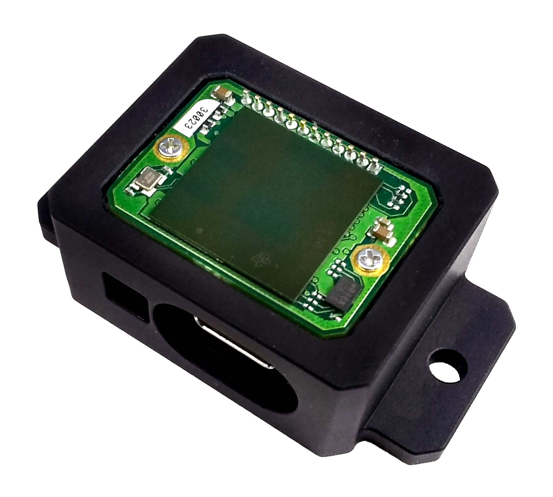
With high-frequency contactless technology operating at 30 to 300 GHz, often known as mmWave is widely implemented as a sensing technology for proximity detection of objects and motion sensing. Since it operates at a high frequency, meaning the technology uses smaller wavelengths that help in giving it high accuracy and is capable of penetrating materials. Due to the increasing demand for industrial and automotive applications, D3 Engineering has announced its DesignCore RS-6843AOPUA mmWave Radar Sensor measuring 1-inch cube form factor. This small form factor sensor with a USB-Serial interface is designed for field testing, sensing evaluation, and algorithm development.
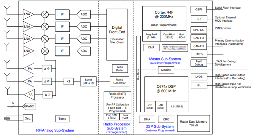
The tiny mmWave radar sensor is based around the ARM Cortex-R4F clocked with up to 200 MHz and Antenna-on-Package AWR6843AOP from the Texas Instrument. The AWR6843AOP single-chip radar device is an AECQ-100 qualified single-chip 60 GHz automotive radar sensor integrated with a DSP and MCU. It also features a radar accelerator and an antenna array in the package.
The processing cores in the AWR6843AOP include a C674x DSP for FMCW signal processing, a hardware accelerator for radar data processing, and a Cortex-R4F microcontroller for object tracking, classification, and communications.
The sensor has two variants, the RS-6843AOPA, and RS6843AOPUA. The former provides an additional option to connect it to baseboards via headers to get more interfaces and functionalities. While RS-6843AOPUA comes with a USB-C connector, which can be used to power the board or enumerate two serial UARTs (one for console and the other for algorithm outputs).
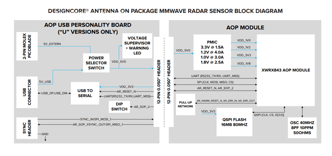
Low-risk solution with block diagram
DesignCore solutions from D3 engineering provides platforms, reference designs, and development tools that are tested and reliable hardware, software, and algorithms. If you are looking for a customizable platform for your application, then the D3 Engineering team can help you quickly move from prototype to design, and then to production.
“The sensor includes custom firmware ensuring board support for the latest version of the SDK from Texas Instrument.”
The RS-6843AOPUA mmWave Radar Sensor is now available for pre-order. However, the cost and expected date of shipping is not provided by the manufacturer, but if you are interested in more information about this, you can contact sales@d3engineering.com.
Radar sensors are not exactly a new thing, but, like every other technology, there is always progress to be made, something that could be improved in order to take the technology to the next level. One of its younger cousins, the mmWave technology, which you may have not heard of until this point, is a promising category of radar sensors that are creeping into, for instance, the automotive industry, with the help of manufacturers such as Texas Instruments. Today, we will take a dive into the mmWave technology, check out what there is so special about it and showcase one product from TI that pushes this technology even further.
Functional block diagram of the AWR6843AOP mmWave sensor from TI
Starting with mmWave (short for millimeter wave), it is a special type of radar that makes use of short-wavelength electromagnetic waves (in the millimeter range, hence the name). By the functioning principle of a radar, you can, through the reflected signals, gather information on range, velocity and angle of objects. The use of millimeter waves is advantageous, in the sense that the required antennas are small and the process is highly accurate, allowing you to detect movements in the fraction of a millimeter. So, where is the catch? Well, designing such a sensor has increased complexity, due to the high frequencies involved (~ dozens of GHz). Then, there is an implementation issue: the antennas, as small as they are, still occupy about 30% of the PCB, according to Texas Instruments. But also, obviously, translates into higher costs, when you consider the need for antenna engineers, the extra sophistication required for the PCB and the size.
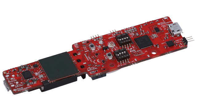
Incredible how much you can cram into a chip these days – AWR6843AOP part
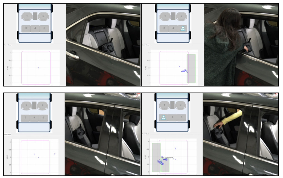
To counter this problem, Texas Instruments provided a new design where the antenna is integrated into the sensor package (Antenna-On-Package, or AOP, if you prefer), which conveniently solves a wide array of problems for you. It drastically simplifies the design and reduces its overall implementation size and cost. So, where can the industry take advantage of this sensor technology, in this smaller form? For example, in robotics applications, you can detect glass walls, which may seem ridicule to mention, but try that with IR sensors or cameras, and you will be surprised to see them struggle. Better odometry is another area where mmWave can shine, and if you ask a robotics engineer, they will take all the help they can get in that regard. The automotive industry can also take advantage of it, for better car seat occupation, intruder detection, among other things (and the smaller size really comes in handy).
Intruder detection in a vehicle’s interior with the help of mmWave sensors
As a finishing note, the mmWave technology is something we need to keep an eye on, as its potential is immense. I have only touched the tip of the iceberg, so if you want to know more about it or what you need to integrate it into your next projects (which starts at around $50, not bad at all), follow the link on the bottom. Have a good one!
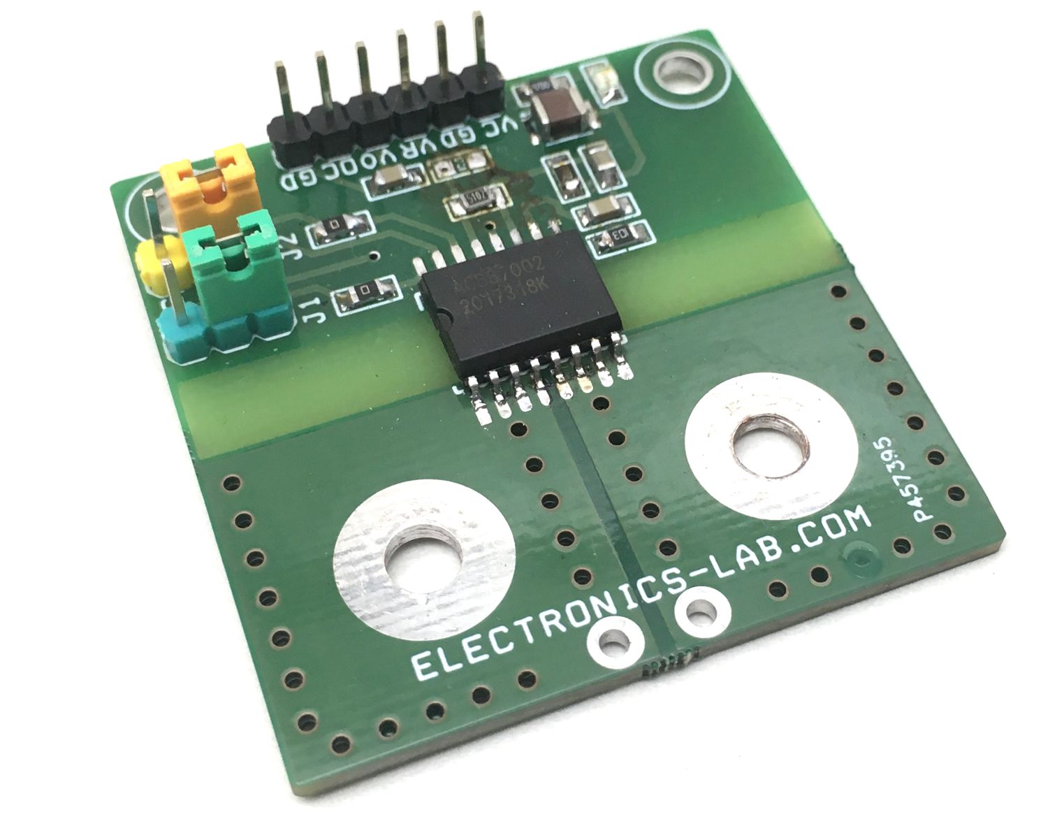
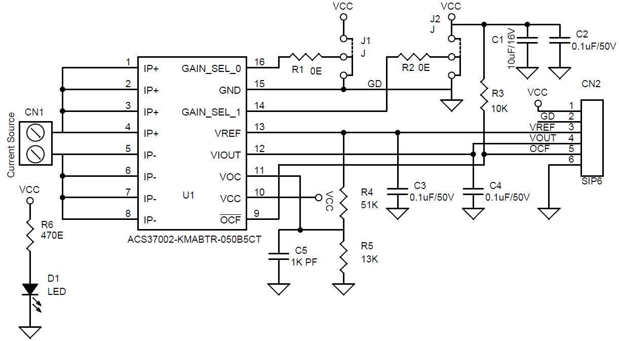
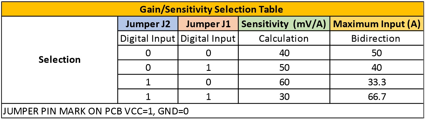
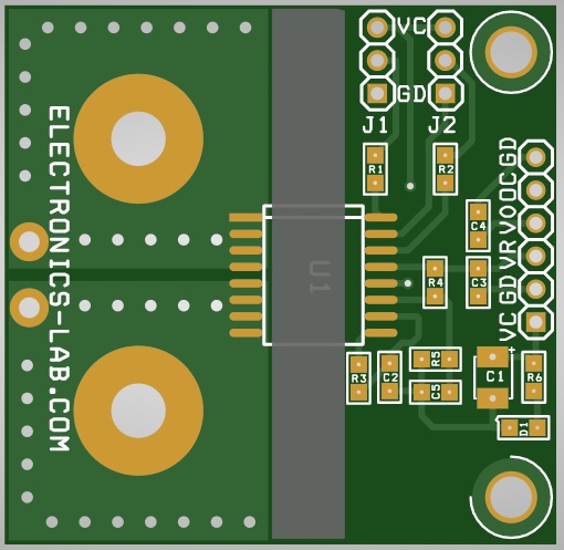
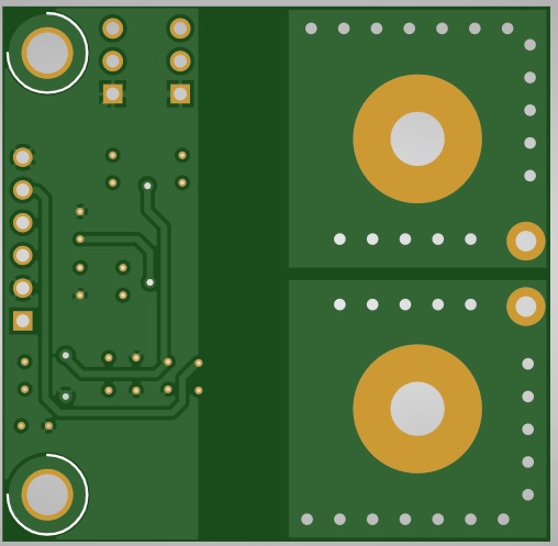
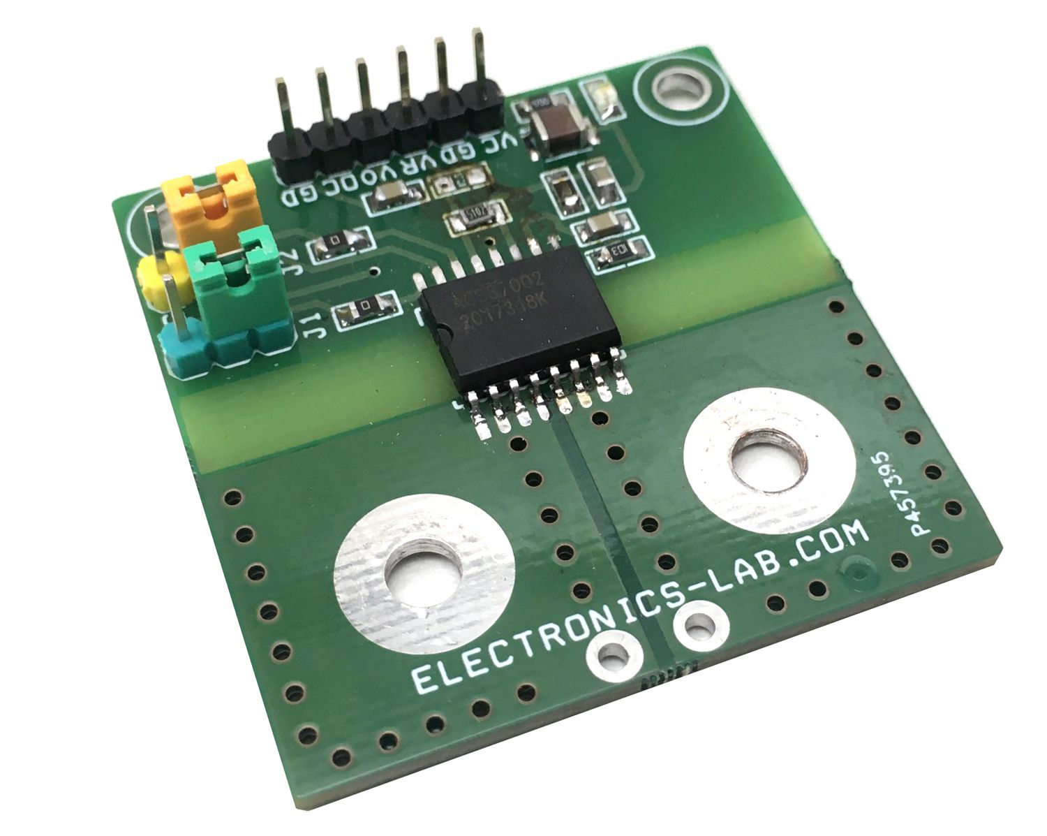
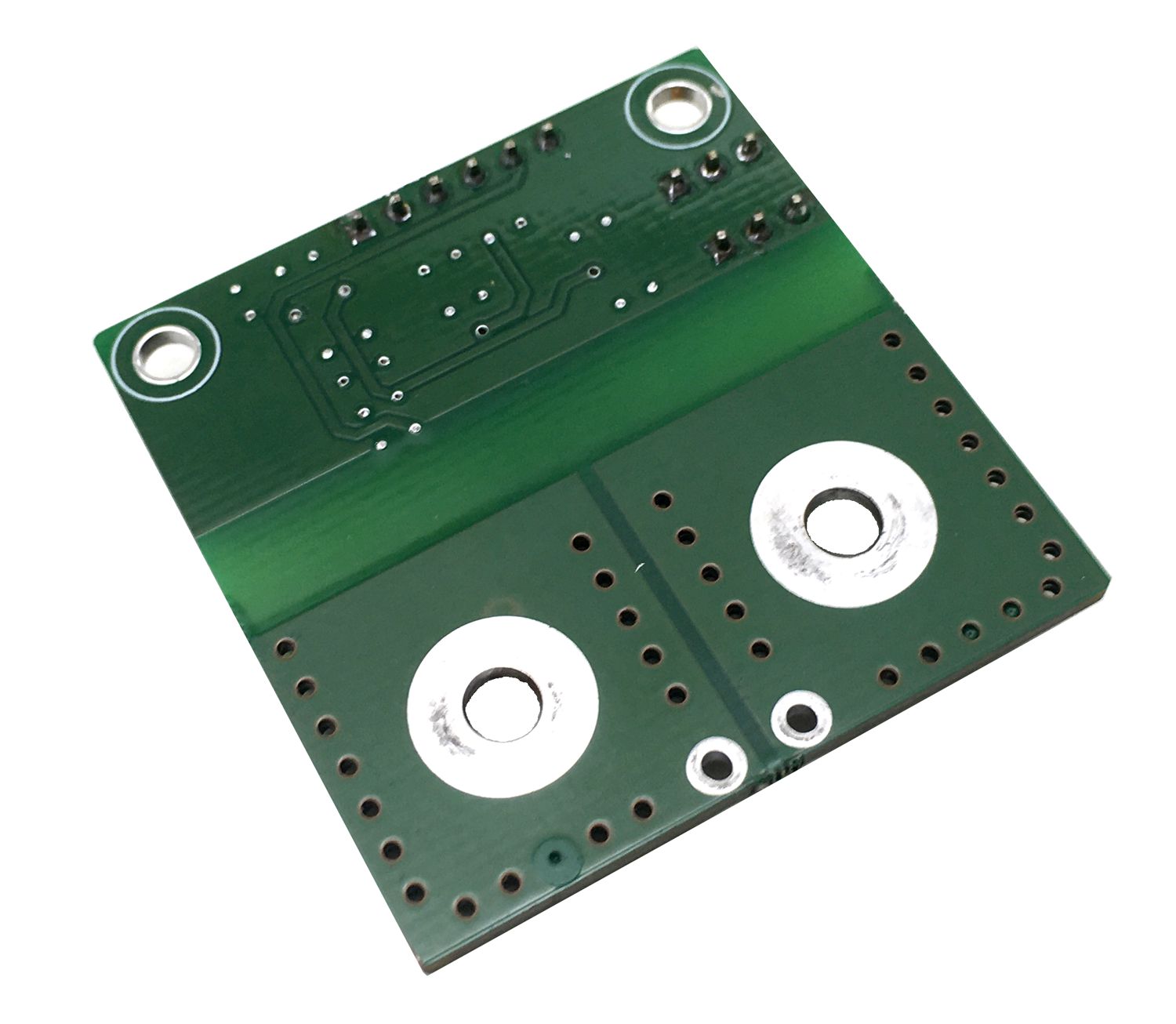
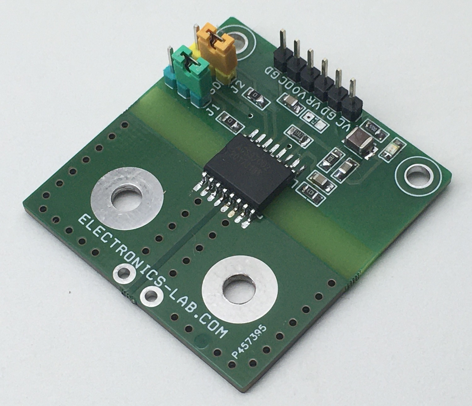
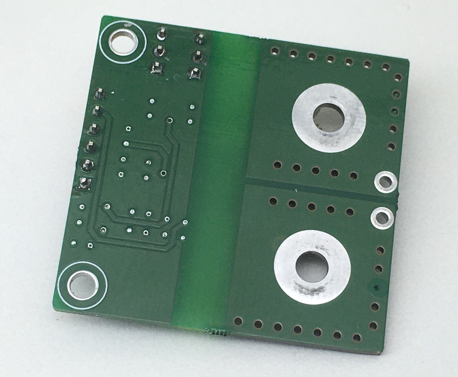
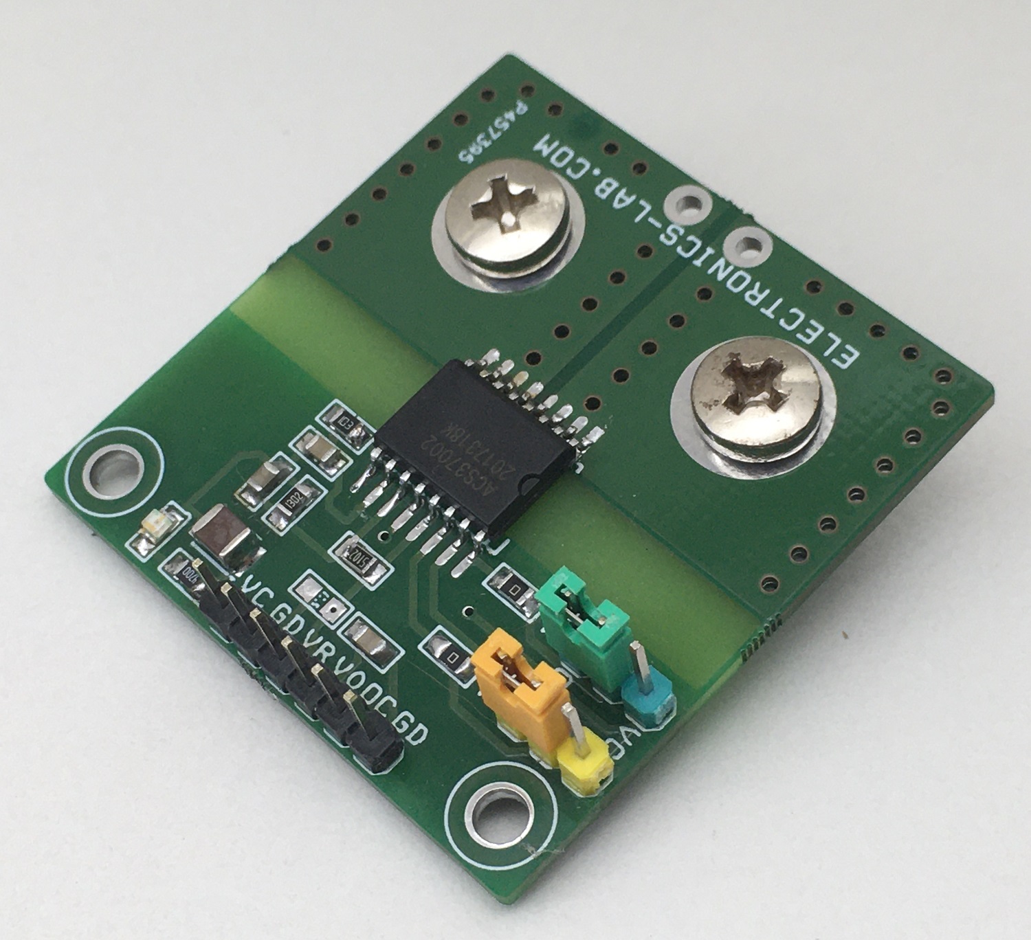
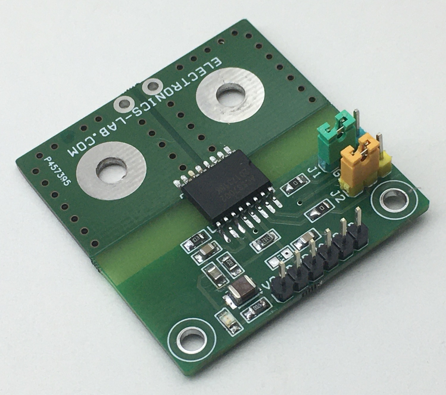
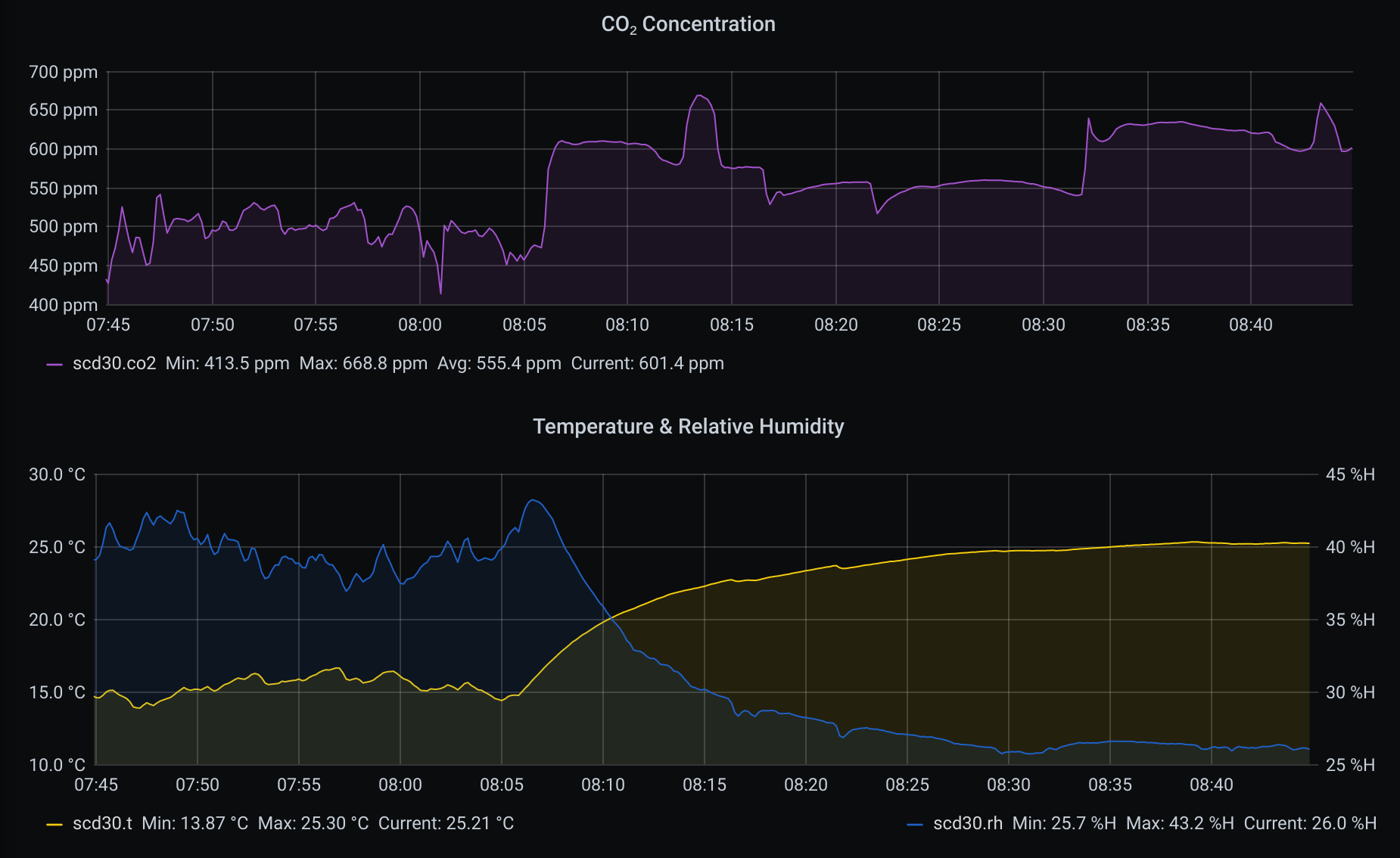
This is a high accuracy current sensor project build using ACS37002 IC from Allegro, which is a fully integrated Hall-effect current sensor with 0.85mOhms integrated conductor. A fast overcurrent alert output, programmable gain settings and analog linear voltage outputs are key features of this project. The sensor has optimized accuracy for current ranges +/-33A to +/-66 A and the analog voltage output is linear for the current of this range. The operating voltage of the project is 5V DC. The output voltage of this sensor is centered at VCC/2 =2.5V. Output sensitivity depends on the jumper settings, please refer to the table below for sensitivity/Gain configuration. CN2 6-pin header connector provided for power input and outputs. D1 is the power LED. Overcurrent alert is set to a minimum but it can be set as per user requirement by changing resistor divider R4 and R5, more information provided below.
Note: It is advisable to change the jumper J1 and J2 settings when the power is OFF. Refer to Jumper setting table for Gain settings
Connector CN2 Connections Details
Pin1=VCC 5V DC
Pin2=GND
Pin3= VREF 2.5V For ADC (Can be used for Microcontroller Interface Left Unused for Stand Alone Use)
Pin4=Sensor Voltage Output
Pin5= Over Current/Fault Output
Connector CN1 = Current Source Connections (Use 5 mm Ring Terminal with 4 mm Screws and Nuts)
Four Configurable Gain Settings Using Jumper J1, J2
Adjustable Fast Over Current Fault 1us Response Time
Over Current Output Normally High Goes Low @ Fault Condition (OCF)
High Operating Bandwidth for Fast Control Loops
400Kz Frequency Bandwidth, 2us Response Time
Very Low Sensitivity Error 1%
6mV Maximum Offset Voltage Over Temperature
PCB DIMENSIONS 42.55 X 41.59 mm
ACS37002: 400 kHz, High Accuracy Current Sensor with Pin-Selectable Gains
The ACS37002 is a fully integrated Hall-effect current sensor in SOICW-16 package that is factory-trimmed to provide high accuracy over the entire operating range without the need for customer programming. The current is sensed differentially by two Hall plates that subtract out interfering external common mode magnetic fields. The package construction provides high isolation by magnetically coupling the field generated by the current in the conductor to the monolithic Hall sensor IC which has no physical connection to the integrated current conductor. The MA package is optimized for higher isolation with withstand voltage, 4.8 kVRMS, and 0.85 mΩ conductor resistance. The LA package is optimized for lower noise with 3.6 kVRMS withstand voltage and 1 mΩ conductor resistance. The ACS37002 has functional features that are externally configurable and robust without the need for programming. Two logic gain selection pins can be used to configure the device to one of four defined sensitivities and corresponding current ranges. A fast overcurrent fault output provides short-circuit detection for system protection with a fault threshold that is proportional to the current range and can be set with an analog input. The reference pin provides a stable voltage that corresponds to the 0A output voltage. This reference voltage allows for differential measurements as well as a device-referred voltage to set the overcurrent fault threshold.
Overcurrent Fault (OCF)
As the output swings, the Overcurrent Fault pin will trigger with an active low flag if the sensed current exceeds its comparator threshold. This is internally compared with either the factory programmed thresholds or via the VOC voltage when VVOC > 0.1 V. This flag trips symmetrically for the positive and negative OCF operating point. The implementation for the OCF circuitry is accurate over temperature and does not require further temperature compensation as it is dependent on the Sens and VOFF parameters that are factory-trimmed flat over temperature.
Overcurrent Fault Operating Range is the functional range that the OCF thresholds can be set in terms of percentage of full-scale output swing. The Overcurrent Fault Operating Point is the specific point at which the OCF trigger will occur, and is set by either VVOC or the factory default setting. The IOCF-OP can be seen in Figure 13 as [9] along with the FAULT pin functionality.
VOLTAGE OVERCURRENT PIN (VOC)
The fault trip points can be set using the VOC pin as the direct analog input for the fault trip point. The VOC pin voltage can be set using R4, R5 resistor dividers from VREF on bidirectional devices. The fault performance is valid when VVOC is within the VOC Operating Voltage Range or <0.1 V. The device will respond to voltage outside of the defined valid performance region with varied results. For a 5 V bidirectional device, setting the VOC pin to 0.5 V selects the minimum trip point, IFAULT (min), and setting the pin to 2 V selects the maximum trip point. Project is set to default minimum I trip point 0.5V, Calculate the Value of R4 and R5 to set the trip point between 0.5V to 2V.
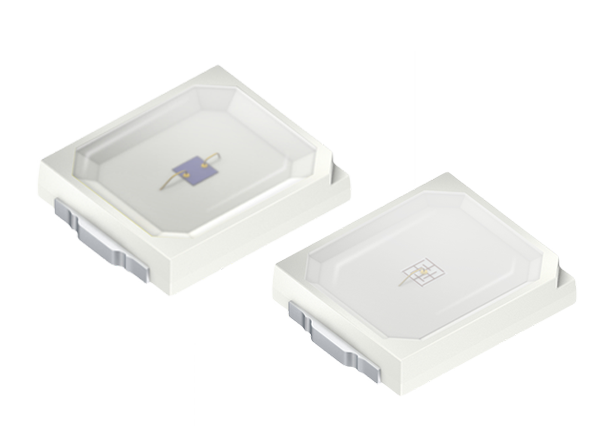
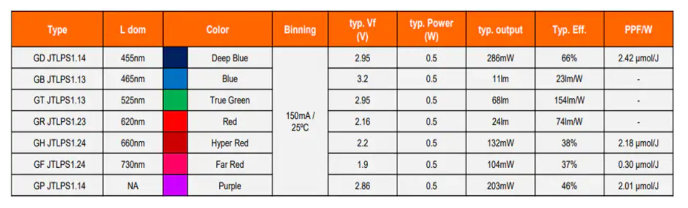
OSRAM Opto Semiconductors DURIS® E 2835 Color LEDs feature excellent color rendering and supreme efficacy in a 2.8 x 3.5mm² PCT package. These color LEDs offer a 120° beam angle and 2kV ESD withstand voltage. The DURIS® E 2835 color LEDs are available in red, green, blue, deep blue, hyper red, far red, and purple colors. Typical applications include architectural lighting, accent lighting, effect lighting, and horticulture lighting.
Features
Excellent color rendering and supreme efficacy
Available in red, green, blue, deep blue, hyper red, far red, and purple colors
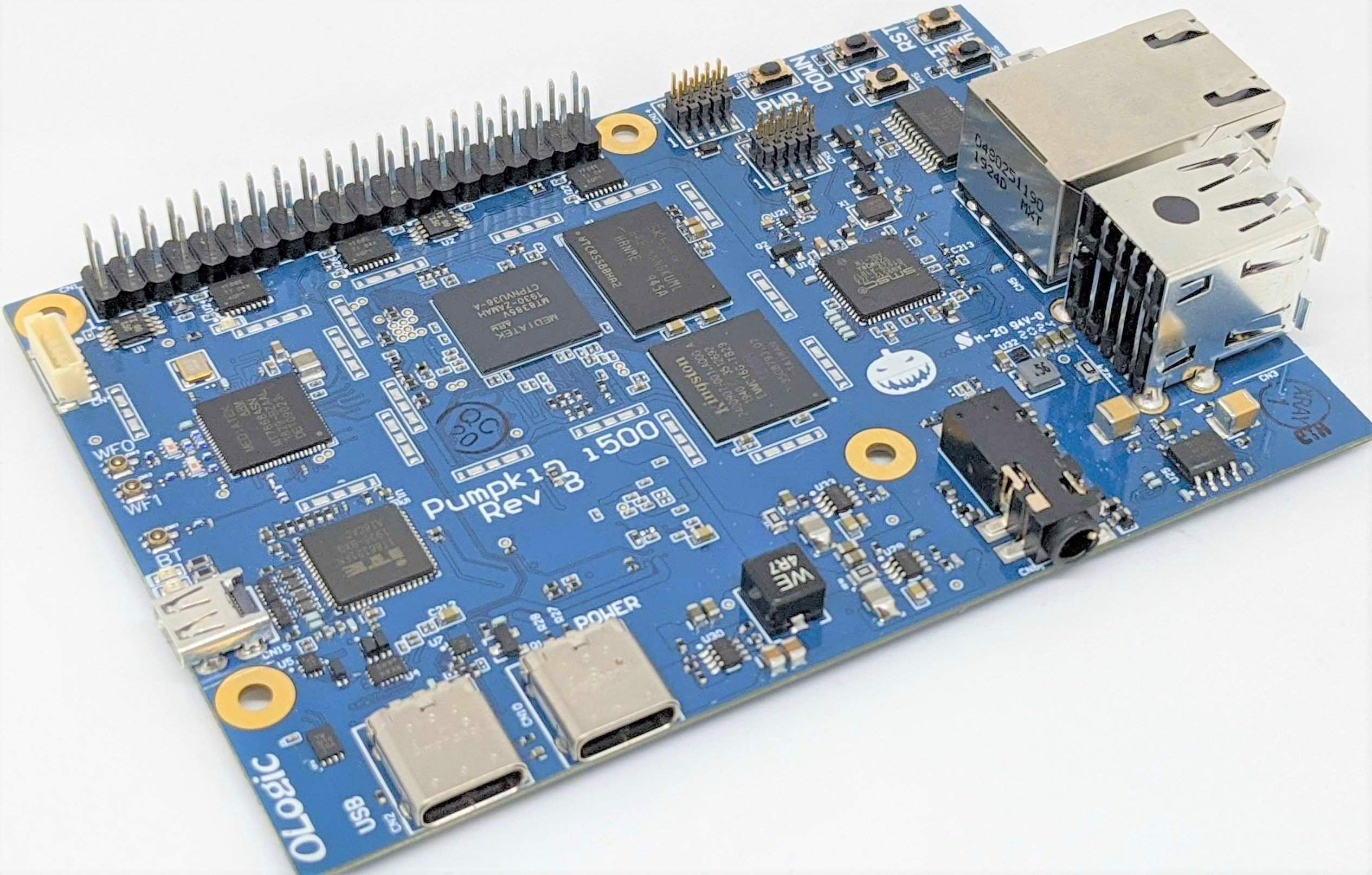
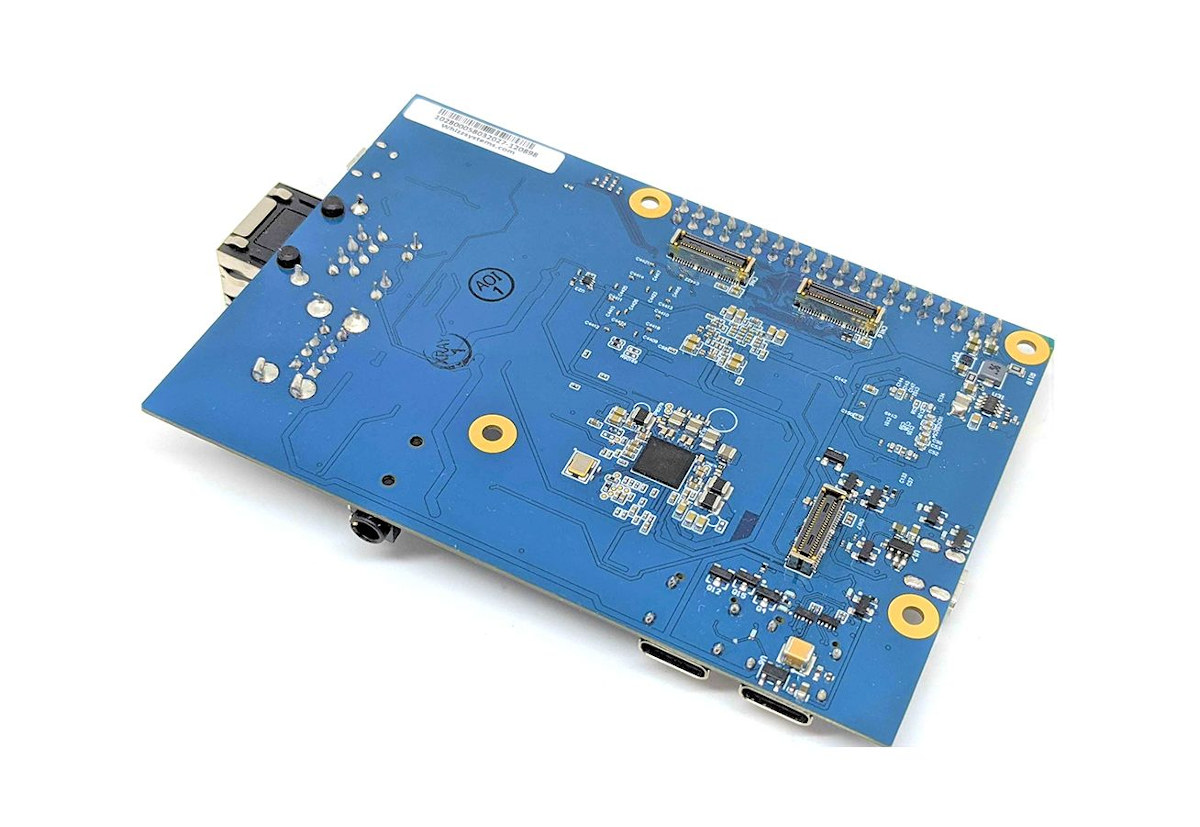
OLogic has released more details on their Pumpkin i500 Single Board Computer built to support computer vision and AI edge computing. The hardware development kit was first announced at the beginning of last year and initially scheduled to launch around that same time but was delayed due to some reasons.
The Pumpkin i500 Evaluation Kit is powered by a powerful MediaTek i500 SoC combined with Quad-core Arm Cortex-A73 and Quad-core Cortex-A53 power-efficient 64-bit CPU solutions together with an Arm Mali-G72 MP3 GPU. The board also features a rich set of GPIO for expandability and a dual-Band Wi-Fi (2.4GHz/ 5GHz) and Bluetooth 5 that make it suitable for indoor/outdoor home and industrial applications.
Features and Specifications of the Pumpkin i500 SBC include:
CPU: MediaTek i500 octa-core processor with quad-core Arm Cortex-A73 running at up to 2.0 GHz and quad-core Cortex-A53 cores at 2.0 GHz
The Pumpkin i500 SBC enables the development of AI vision products like control panels, smart appliances, points-of-sales, smart hubs, robots etc. Users can also easily deploy their workloads to the Edge through standard containers because the board is qualified for AWS IoT Greengrass and certified for Microsoft Azure IoT Edge.
The manufacturer of the board provides support for Yocto Linux and Android 10 operating systems using Linux 5.4 kernel, as well as support for TensorFlow Lite and object detection with MobileNet and SSD models. This affords third party customers the opportunity to test AI models and Computer Vision algorithms on top of the base layer. Support for software is also provided through the Pumpkin Software SDK which is equally supported by BayLibre.
More details on the Pumpkin i500 SBC can be found on the company’s product page or on Seeed Studio where the board was listed to sell for $299.
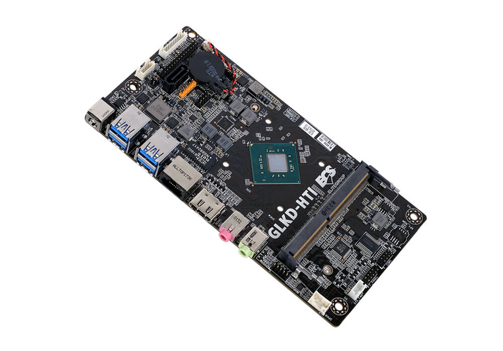
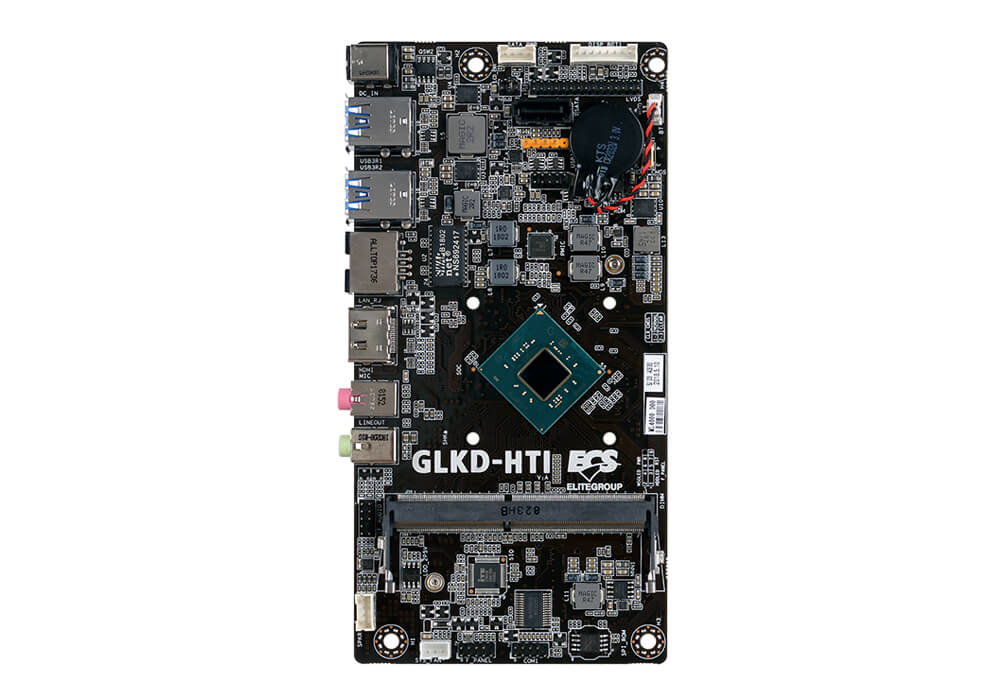
So… Odd title, right? Well, not quite! Today we will be analyzing an ambitious idea from Elitegroup Computer Systems (ECS, for short), which takes a Mini-ITX board and shrinks it to half its original size. As a cool concept this is, does it have enough “glue” to stick on everyday’s market of computers? Let us figure that out.
The GLKD-HTI motherboard, developed by ECS, creates a new concept, as we discussed. Some are baptizing it as “Half Mini-ITX”, which is not a bad name, but the nomenclature should change if this becomes more popular. At least, I think it deserves a better name. Never-mind. This Intel-based CPU on Board solution is quite unique, on the sense that it carries most of what you would expect of Desktop computer hardware and places it into a small package. One of my first questions when I saw this was: how did they solve the power supply? Because we are used to seeing those bulky boxes delivering power to the computers, unless they are laptops. Then, I looked closely to the specs and noticed the 12 V DC connector. Another question, and this one is a bit trickier: as this form factor is quite unusual, is there any off-the-shelf case for it? The answer is a simple, obvious and sad no. But it might not be the intent for it. Since it is a unique piece of hardware, you may want to apply it to a unique situation.
Graphics: Onboard Intel HD Graphics 600 (with support for DirectX 12 and HDMI 1.4a)
Memory: Support for single-channel, 8 GB DDR4 memory, up to 2133 MHz
Storage and expandability: 1x M.2 slot for SSD + 1 x M.2 slot for Wi-Fi / Bluetooth PCIe Gen 2
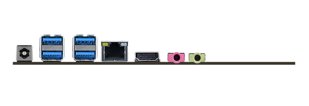
Rear I / O: 2x audio jacks (line out and mic in), 1x RJ-45 port, 1x HDMI 1.4a port, 4x USB 3.0 port and 1x DC 12 V connector
Realiability: 100% solid capacitor design, ECS Durathon technology for stability + reliability and performance + ESD protection
OS: Windows 10 64-bit
Form factor: 170 x 85 mm
A glance at the GLKD-HTI I / O
From the list of specifications, you may get some mixed feelings, if you planned this one to be your next daily driver. In my opinion, it is not up to it. There are some small caveats, such as only 8 GB of RAM, no USB Type-C, or the option for better graphics… But is that the point here? Not really. Imagine using those 12 V DC for the graphics card, it just would not work like that, it requires a PSU and there goes the portability out the drain. But it can suit in many other places: media centers, something to have near a television, it certainly has that potential. When it comes to pricing, there is no information yet, as it still is in the works. As final thoughts, where do you see this one fit?
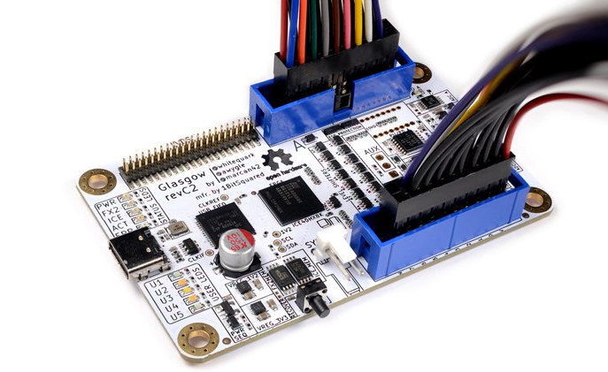
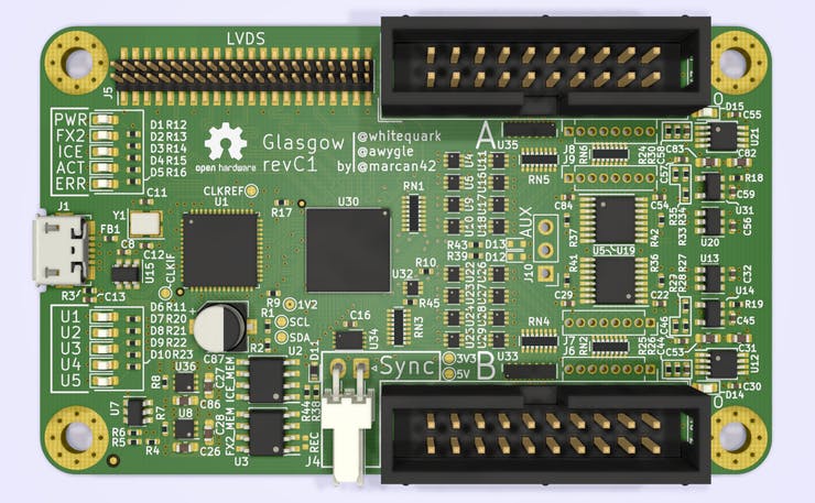
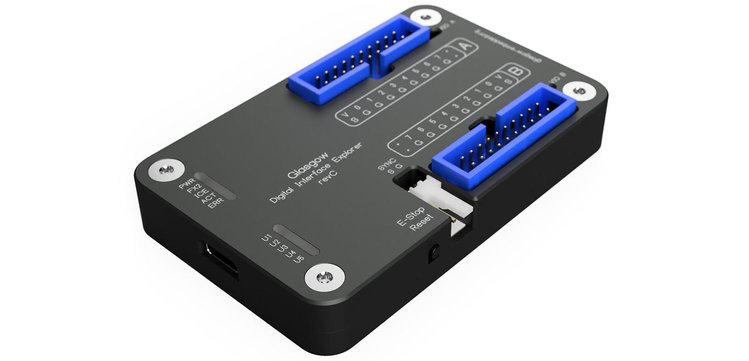
1BitSquared has launched a crowdfunding campaign for a highly capable and extremely flexible open source multi-tool called Glasgow Interface Explorer.
Glasgow Interface Explorer for digital electronics is powered by Lattice Semi iCE40 FPGA and created for hardware developers, electronics hobbyists, engineers, tinkerers, and
“anyone else who wants to communicate with a wide selection of digital devices with minimum hassle.”
The board aims to offer a broad selection of capabilities with more than “some wires and, depending on the device under test, external power.” You can attach it to devices without any need for extra active or passive components.
Some of its Key Features and Specifications include:
iCE40HX8K Lattice Semiconductor FPGA
1x USB-C port connected to FX2 high-speed USB interface; 480 Mbps throughput
2x 8-channel GPIO banks, each with:
A dedicated programmable linear voltage regulator, configurable from 1.8 – 5V with up to 150 mA of power
A dedicated sense ADC capable of monitoring the GPIO bank voltage and current, with interrupt trigger thresholds that can be set
16 highly flexible GPIOs, each with:
A peak frequency of 100MHz
A dedicated level shifter with individual direction control, and,
An independent, software-controlled 10K Ohm resistor Pull-Up/-Down resistor
ESD protection diodes for all GPIOs
Set of 14x differential pair I/O, connected directly to the FPGA (optional); can be used for high speed interfaces
Up to 5x User-controlled LEDs
Up to 5x Status LEDs, and,
1x Dedicated SYNC connector
The software is fully in Python 3, including the FPGA logic, which is described with a Python-based domain-specific language.
“The Glasgow software is a set of building blocks designed to eliminate incidental complexity. Each interface is packaged into a self-contained applet that can be used directly from the command line or integrated into a more complex system. Using Glasgow does not require any programming knowledge, though it is much more powerful if you know a bit of Python.”
says 1BitSquared.
Glasgow is highly flexible since it is based on an FPGA, and can do a number of things like:
Communicate via UART with automatic detection of the baud rate required
Initiate SPI and I2C transactions
Read and write to and from 24-series electrically erasable programmable read-only memories (EEPROMs)
Read and write 25-series flash memories
Read and write any ONFI-compatible flash
Program and verify AVR microcontrollers over SPI
Play back JTAG SVF files
Debug ARC processors over JTAG
Debug a subset of MIPS processors via EJATG
Program and verify XC9500XL CPLDs
Determine unknown JTAG pinouts automatically
Read raw modulated data from 3.5″ and 5.25″ floppy drives
The board is currently available through a crowdfunding campaign that was launched recently on Crowd Supply with a USD 25,000 funding goal. The campaign has so far raised more than USD 154,000 with over 850 backers and it will still be on for the next one month. You can get the latest RevC revision of the board with a full set of flywire, sync, and USB-C cables for $139 and another package with an optional CNC-milled and anodized aluminum case for $189.
The project is also entirely open source, and all hardware design files, firmware, software and documentation are available on Github.
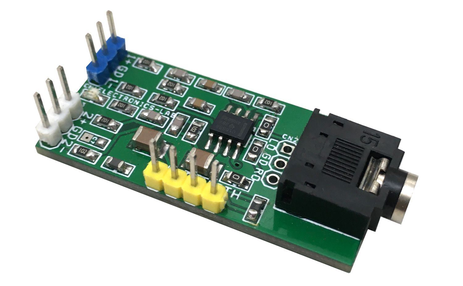
This is a headphone amplifier project for audio digital-to-analog converters (DACs) with differential voltage outputs. This circuit converts the differential voltage output of the DAC to a single-ended, ground-referenced signal and provides the additional current necessary for low-impedance headphones. Project is built using OPA1688 low distortion, high-drive Sound Plus audio amplifier. The circuit tested with dual +/-5V DC supply, and it can drive a load 16 Ohms to 600 Ohms. Headphone amplifier provides an output 50mW into 32 Ohms. Signal for the right channel and left channel input is applied to the amplifier through connectors CN1and CN3, respectively.
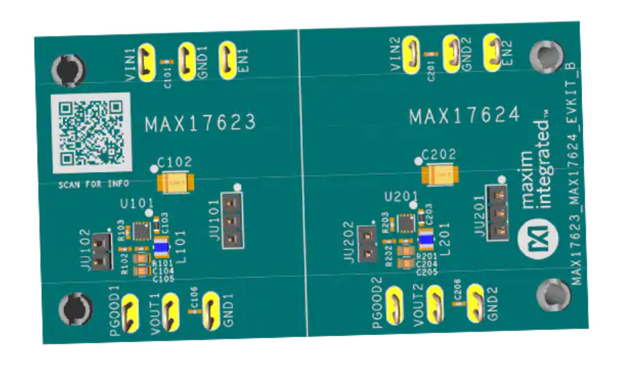
Maxim Integrated MAX17623/MAX17624 Evaluation Kits is configured to evaluate the MAX17623/MAX17624 Step-Down Converters’ operation. The MAX17623/MAX17624 Step-Down Converters are part of the Himalaya series of products that enable cooler, smaller, and simpler power supply solutions. The devices are configured to demonstrate optimum performance and component sizes in the Evaluation Kits.
The Maxim MAX17623/MAX17624 Evaluation Kits feature provisions for selecting the mode of operation (PWM/PFM), enabling or disabling the output and PGOOD signal.
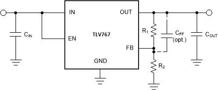
Texas Instruments TLV767 Precision Positive Voltage Linear Regulators are a wide input linear voltage regulator that supports an input voltage range from 2.5V to 16V and up to 1A of load current. The output range is from 0.8V to 6.6V or up to 13.6V in the adjustable version. Additionally, the TLV767 has a 1% output accuracy that can meet the needs of low voltage microcontrollers (MCUs) and processors.
The TLV767 is designed to have a much lower IQ than traditional wide-VIN regulators, thus making the device well positioned to meet the needs of increasingly stringent standby power requirements. When disabled, the TLV767 draws only 1.5µA of IQ. The internal soft-start time and fold-back current limit reduce inrush current during startup, thus minimizing input capacitance.
Features
VIN: 2.5V to 16V
VOUT
0.8V to 13.6V (Adjustable)
0.8V to 6.6V (Fixed, 50mV Steps)
1% Output Accuracy Over Load and Temperature
Low IQ: 50µA (Typical, ~1.5µA in Shutdown)
Internal Soft-Start Time: 500µs (Typical)
Fold-Back Current Limiting and Thermal Protection
Stable With 1µF Ceramic Capacitors
High PSRR: 70dB at 1kHz, 46dB at 1MHz
Temperature Range: –40°C to +125°C
Package: 6-Pin 2mm×2mm WSON
Wide bandwidth PSRR performance is greater than 70dB at 1kHz and 46dB at 1MHz, which helps attenuate the switching frequency of an upstream DC/DC converter and minimizes post regulator filtering. To allow for more flexibility, the TLV767 has both fixed and adjustable versions.