Introduction
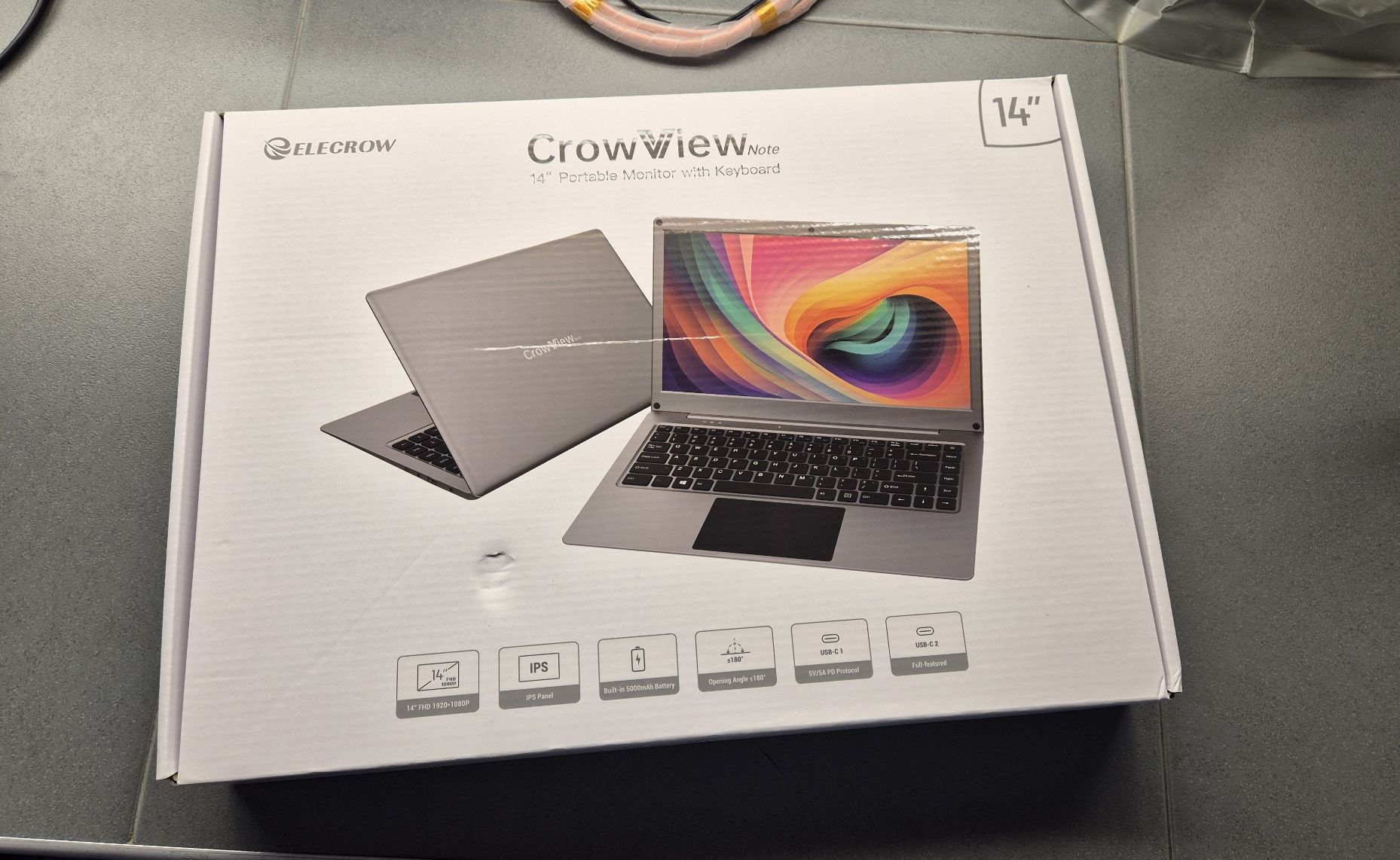
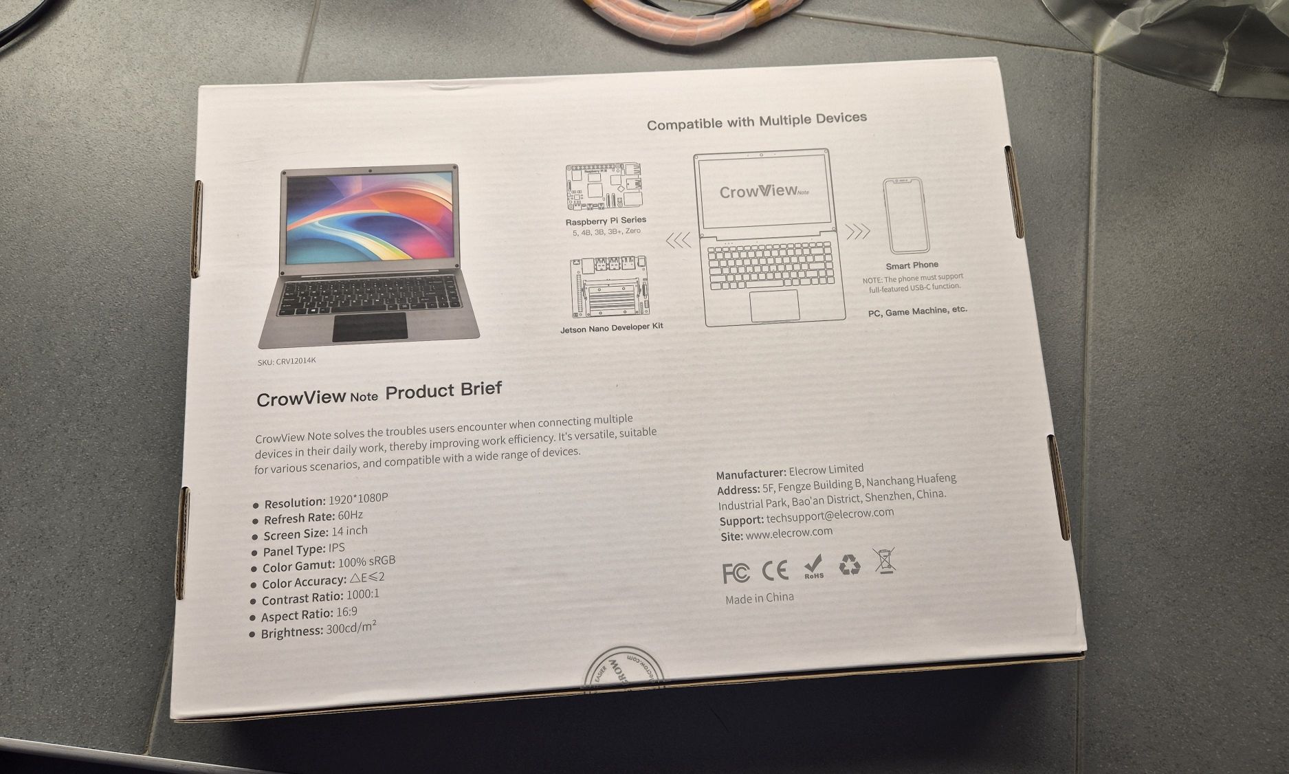
The CrowView Note – 14” is a portable laptop-style monitor with an integrated 14-inch Full HD (1920×1080) IPS display (100% sRGB color gamut) along with a keyboard, touchpad, and speakers. The device easily connects with gadgets like smartphones, computers, Mini PCs, and single-board computers (SBC) like the Raspberry Pi and Nvidia Jetson Nano, etc. It has a built-in 5000mAh battery and can normally work for 1-2 hours without any external power supply. Moreover, the built-in battery can also power smartphones, Raspberry Pi, and other devices. Forget carrying out a heavy laptop or your expensive MacBook on your trip, because, with this compact portable device, you only need to connect your smartphone and do your major work. The best part is it will only cost you hundreds, not thousands that you may spend on an expensive laptop.
Packaging
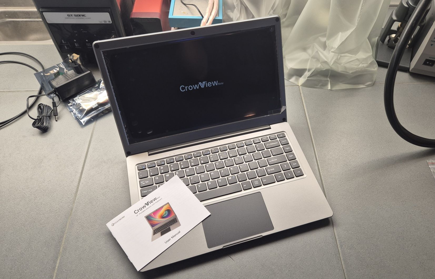
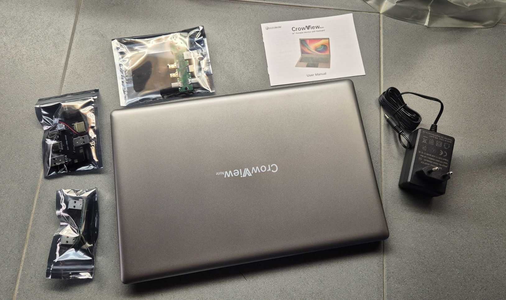
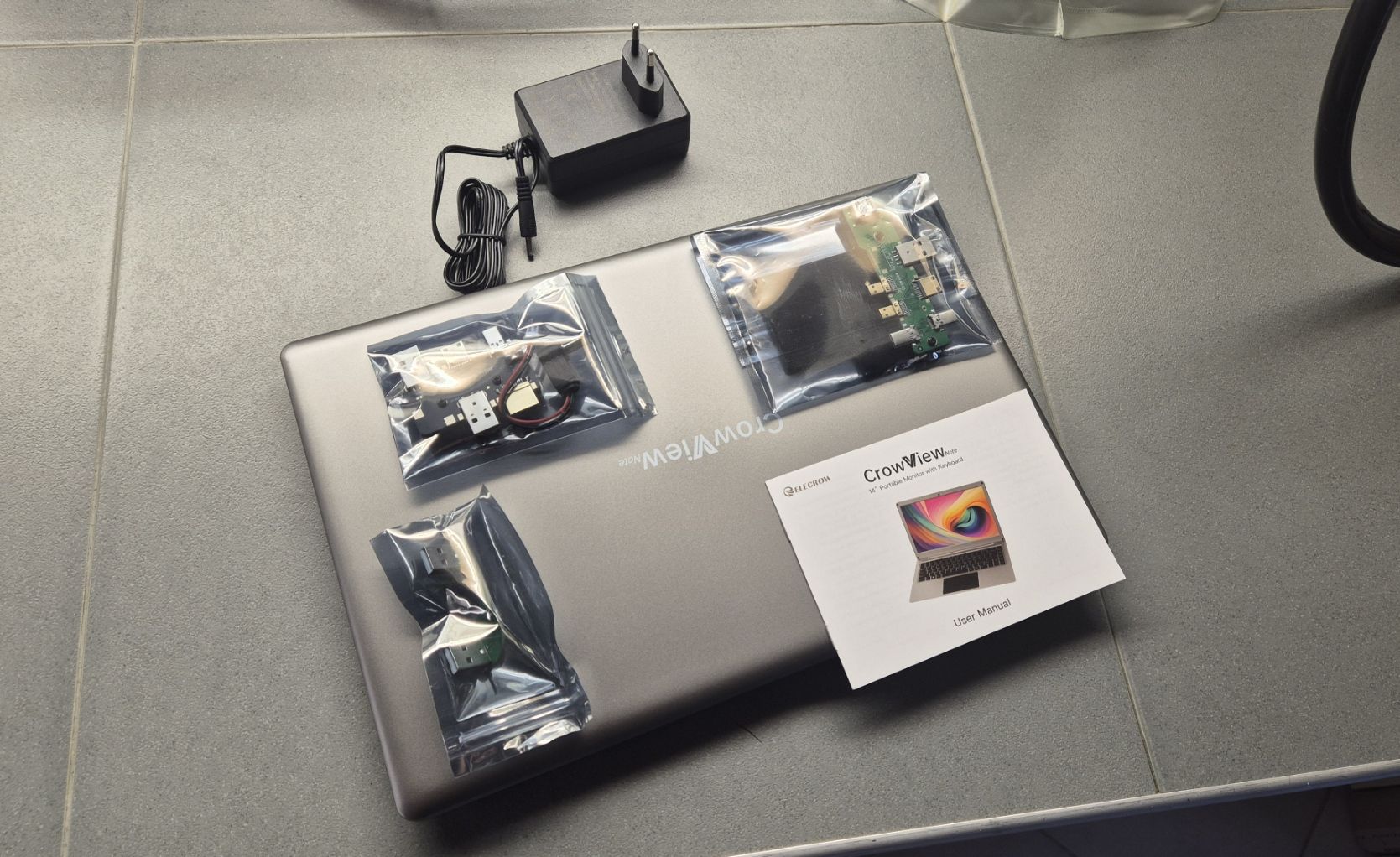
The CrowView Note package comes complete with everything you need to get started. In the box, you’ll find the CrowView Note, a handy user manual to guide you through setup and features, and a convenient adapter to ensure compatibility with your devices.
Design and Build
Talking about the design and build quality of the device, it has a sleek and modern design, resembling a compact laptop, this all-in-one design includes an integrated screen, keyboard, touchpad, and speakers. Which makes it a good choice for those users who require a multifunctional portable display. The plastic case quality seems robust and has a nice gray paint finish, which it’s uncertain if it will last for the lifetime of the product. Overall quality feels like a mid-range laptop, and for sure you have to pay attention while carrying it from one place to another.
Display Quality
The CrowView Note -14” has a 14-inch Full HD (1920×1080) IPS display with a 100% sRGB color gamut, which translates to vibrant colors and sharp visuals. The screen brightness is 300 cd/m2, which makes it easy to see in different lighting conditions. The standard aspect ratio is 16:9 like most modern displays, providing enough screen for multitasking and media consumption. One effective feature is connecting this device to a smartphone and using it like a desktop, basically turning it into a computer. This is basically for those people who use their phones for work and need a bigger screen to do more things. The quality of the display is sharp and crisp and you would enjoy working on it.
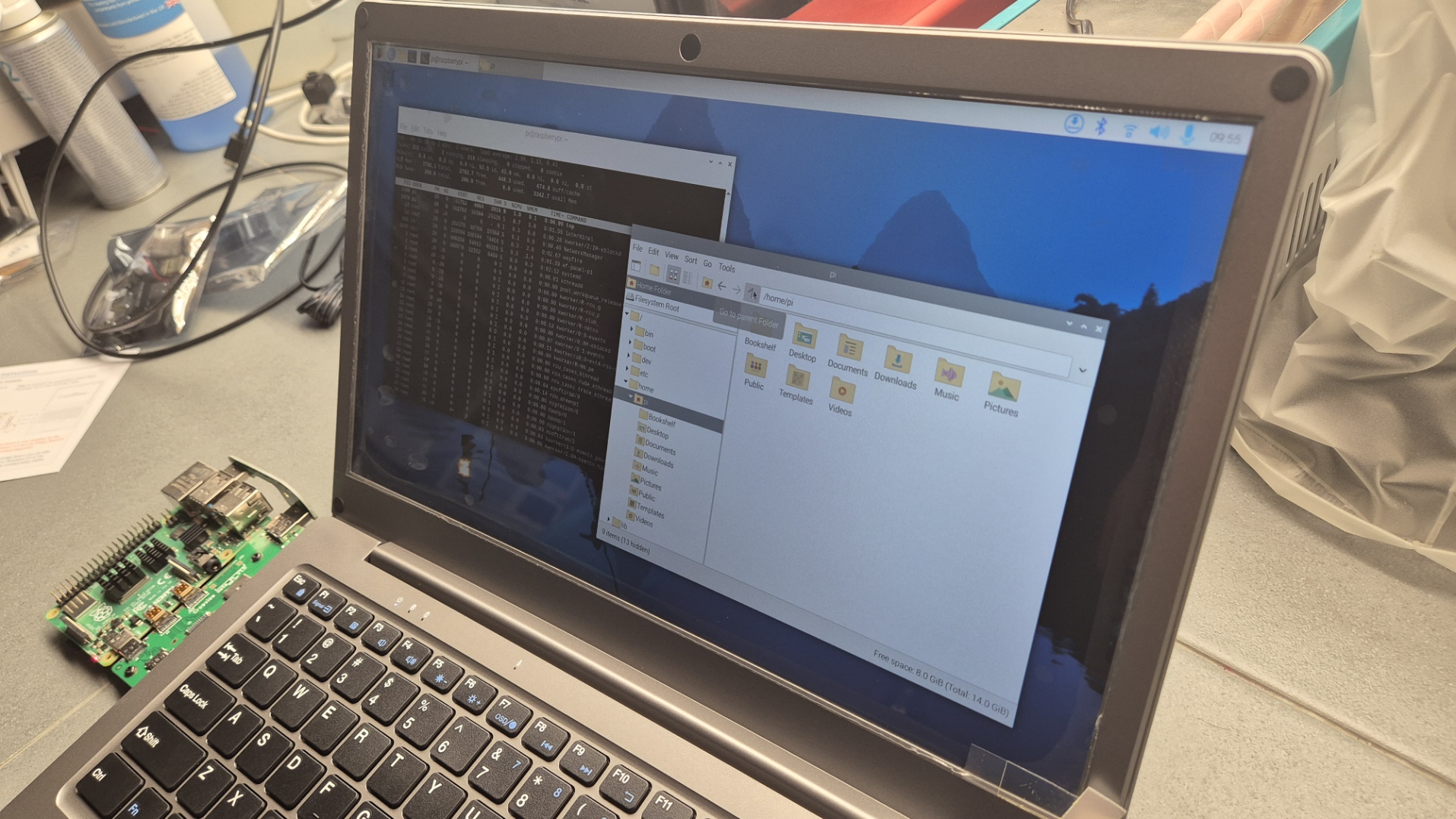
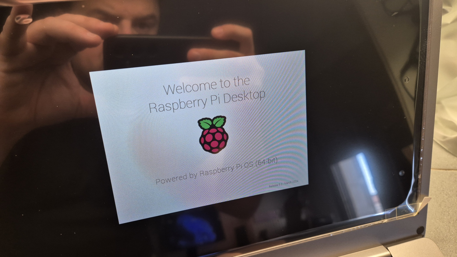
The device supports multiple operating systems, including the latest version of Windows, Mac, Chrome, Linux, Android, Switch, PS4/PS5, and Raspberry Pi. On top of that, the notebook can connect via USB Type C (with DisplayPort Alt Mode) or Mini HDMI, which means you can connect your laptop, Mini PC, and other compatible devices. The list of compatible devices makes this device usable for those who need a portable screen with a keyboard and touchpad for work, Gaming, or Entertainment.
Connectivity
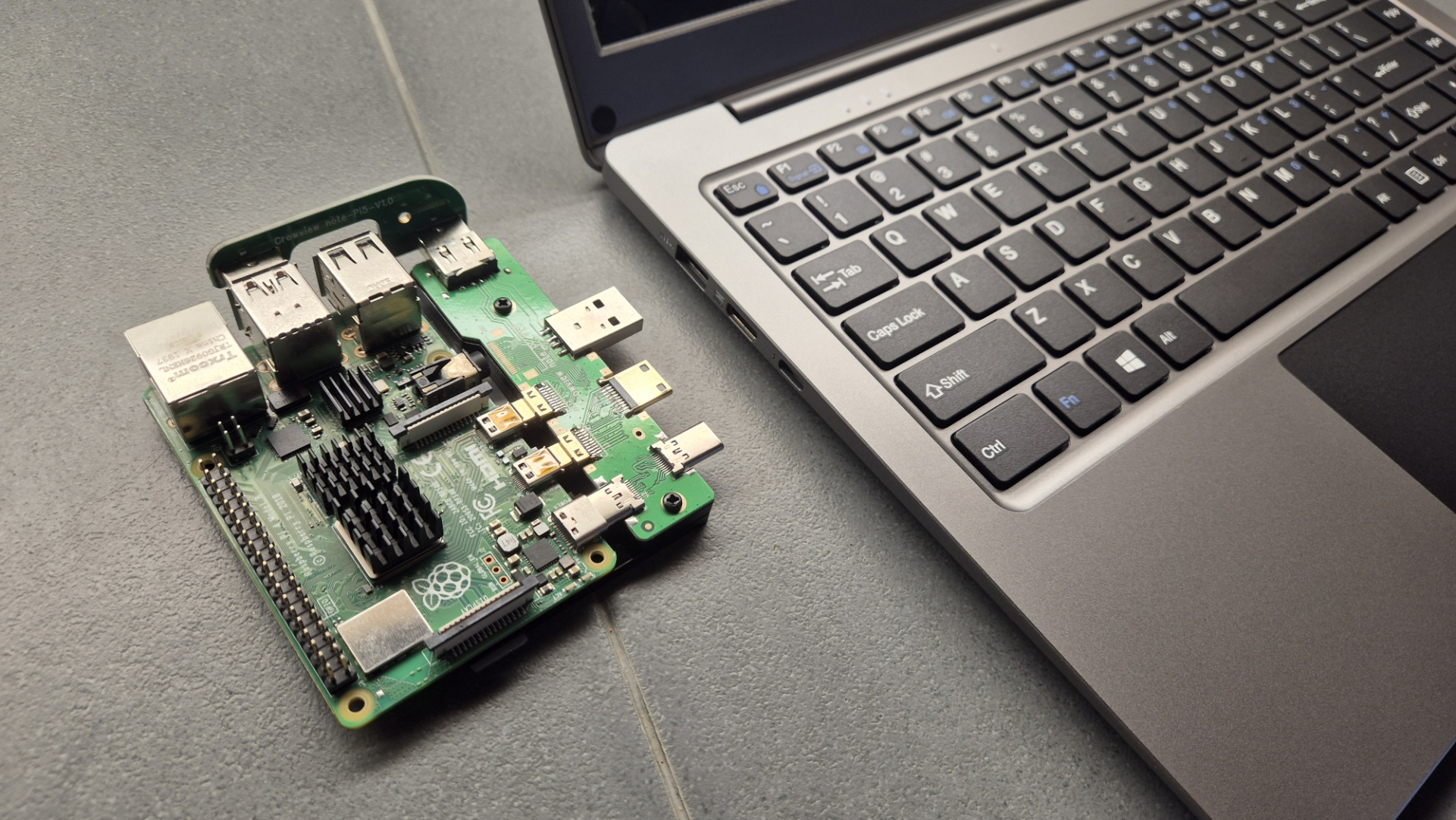
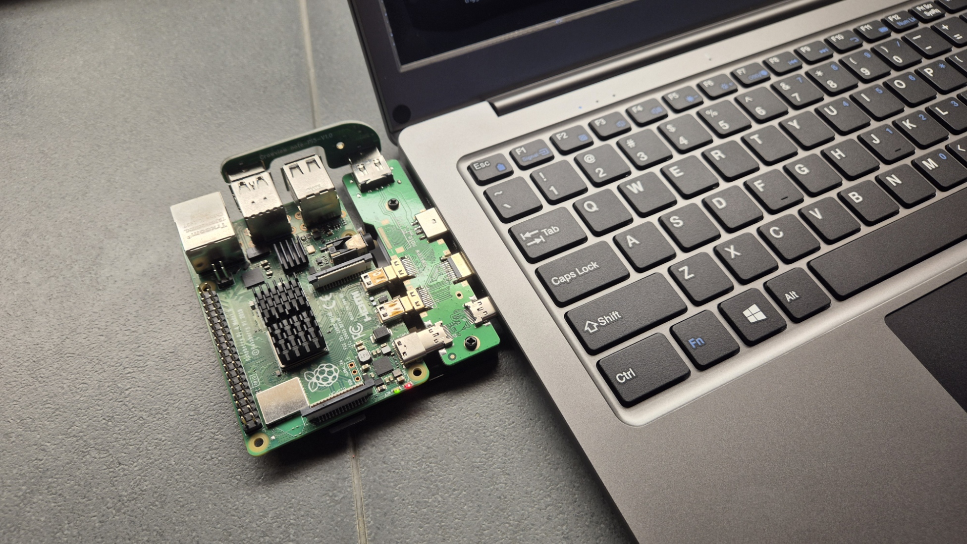
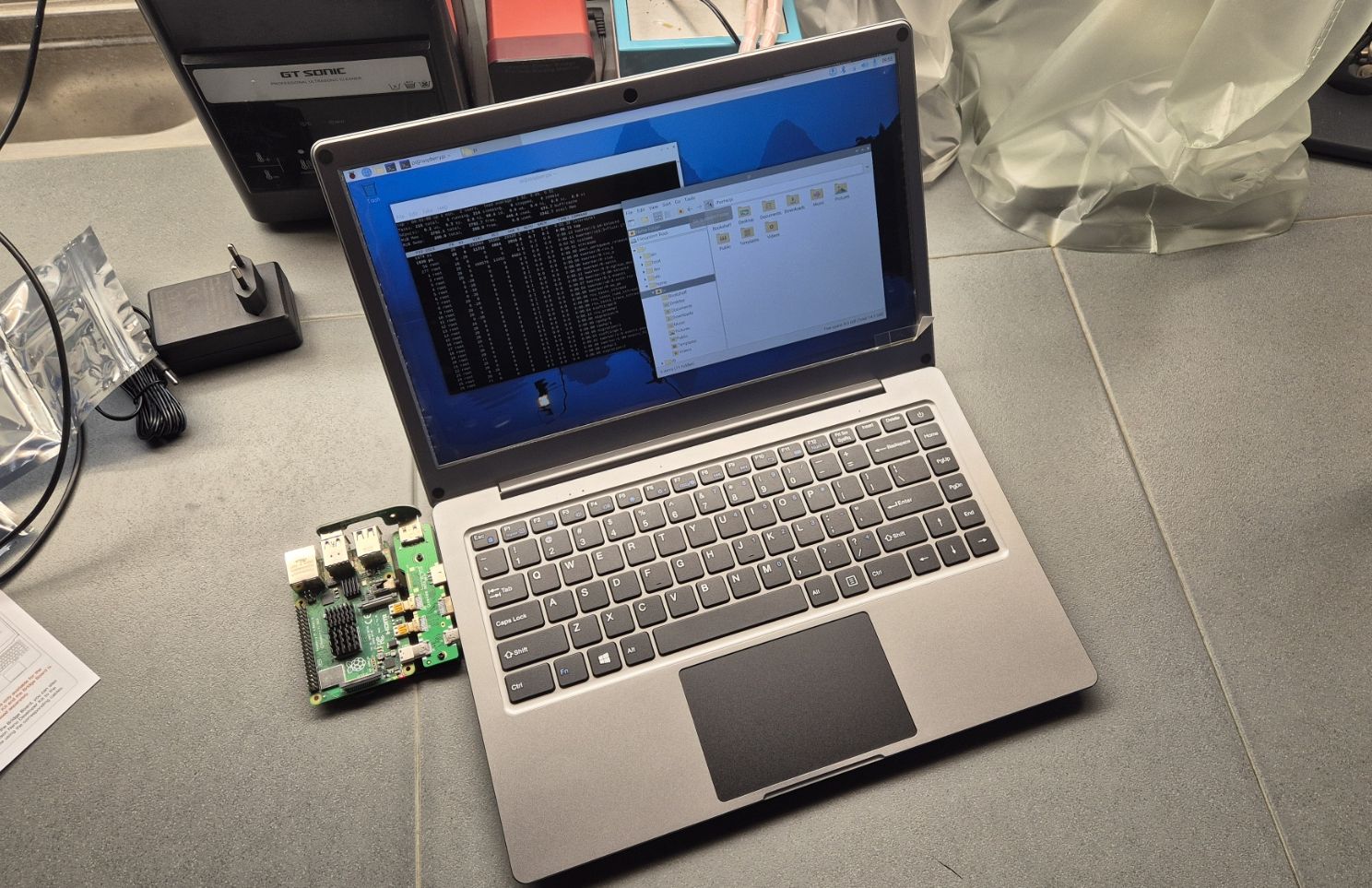
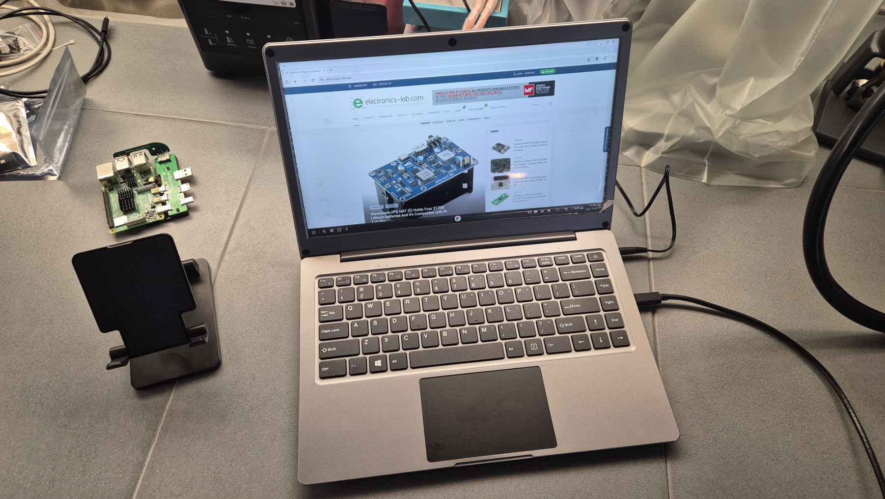
Not only multiple operating systems, the device also supports various SBCs making it a great choice for those using devices like Raspberry Pi, Rock Pi, Beagle Bone, Latte Panda V1, Nvidia Jetson Nano, Orange Pi 4B, and Banana Pi MS. The monitor’s support for HDMI and USB Type C connections ensures that it can easily interface with SBCs that feature these ports. This device works smoothly with other gadgets like gaming consoles and laptops, you can use it for different purposes. It’s also great for people who use those tiny but powerful computer boards called SBCs. Programmers, hobbyists, and teachers can use this device for coding, building projects, or watching videos. The display is very handy because it connects easily to most devices with HDMI or USB-C and gives you a practical solution for increasing your workspace.
The CrowView Note connects with multiple devices, making it a very flexible tool for everyone in daily life. It has ports for USB-A (to connect devices and your main computer), Mini HDMI (for video), and Type-C (for both power and data). You can even plug in your headphones for audio and use a separate power supply if needed. This device works smoothly with all sorts of gadgets like laptops, smartphones, and Mini PCs from well-known brands like Apple, Samsung, Huawei, Dell, HP, and Lenovo. Whether you’re super tech-savvy or just starting, the CrowView Note is super handy.
CrowView Note -14 Inch has multiple interfaces including a USB type C port, a Mini HDMI port, and a USB-A port with a 3.5 headphone port. The USB type C port is used for both power and data transmission with just one cable. This makes it convenient for connecting to laptops and other devices that support USB type C. The Mini HDMI port is very useful for connecting to Gaming consoles, Raspberry Pi, and other devices with HDMI outputs. Additionally, the USB type A port can be used for connecting peripherals or for data transfer. This range of ports allows this device to connect easily to multiple devices like Laptops, Smartphones, and Gaming Consoles. Whether you’re using it for work, Gaming, or presentations, these multiple interfaces provide flexibility and convenience.
Other than that the device offers a variety of ports and connectivity options, making it flexible for different use cases. Here are the main ports and their functions:
- USB-C Port: This port supports both power and data transmission, allowing for a single-cable connection to compatible devices. It can be used to connect the monitor to laptops, smartphones, and other USB-C equipped devices. This simplifies setup and reduces cable clutter, as it can handle video, audio, and power simultaneously.
- Mini HDMI Port: The Mini HDMI port is available while connecting the monitor to devices like gaming consoles, cameras, and other systems with HDMI outputs. This port supports High-definition video and audio, making it ideal for gaming, media playback, & other applications that require high-quality visuals.
- USB-A Port: This port can be used for connecting peripherals such as a keyboard, mouse, or USB storage device. It provides additional flexibility for those who need to connect accessories while using this portable device.
Performance
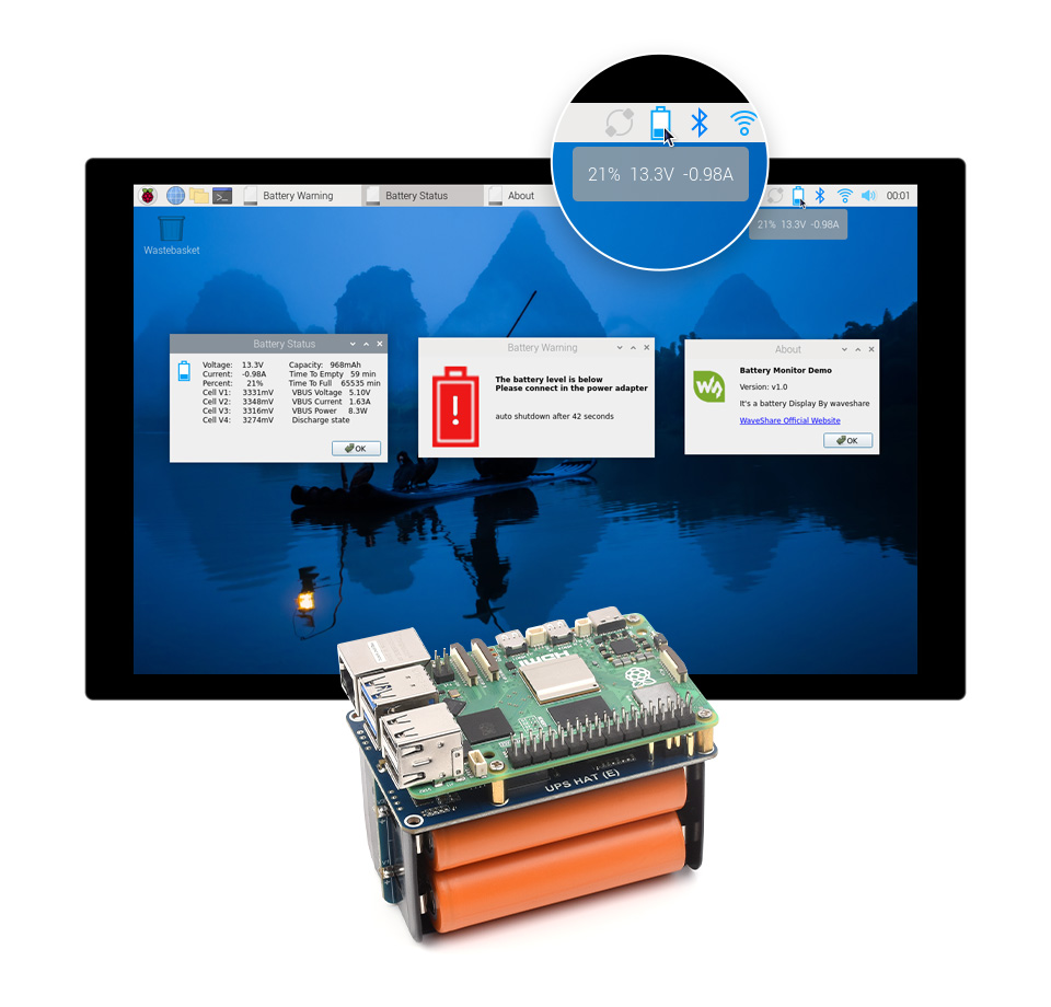
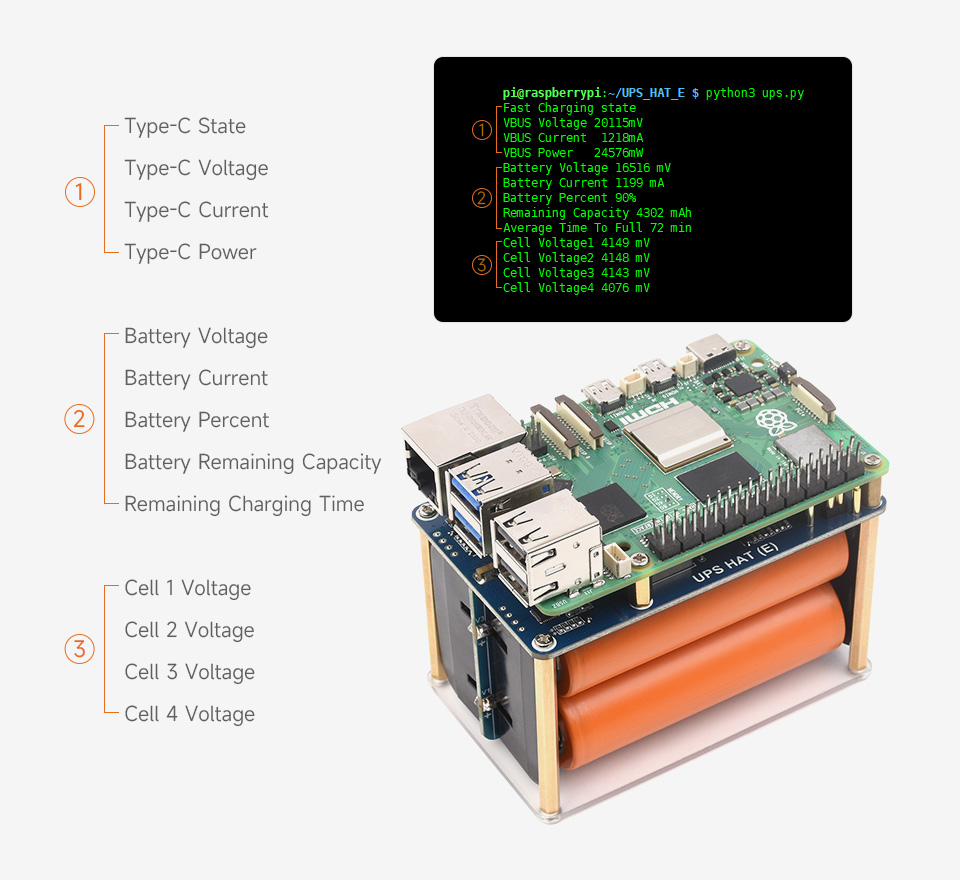
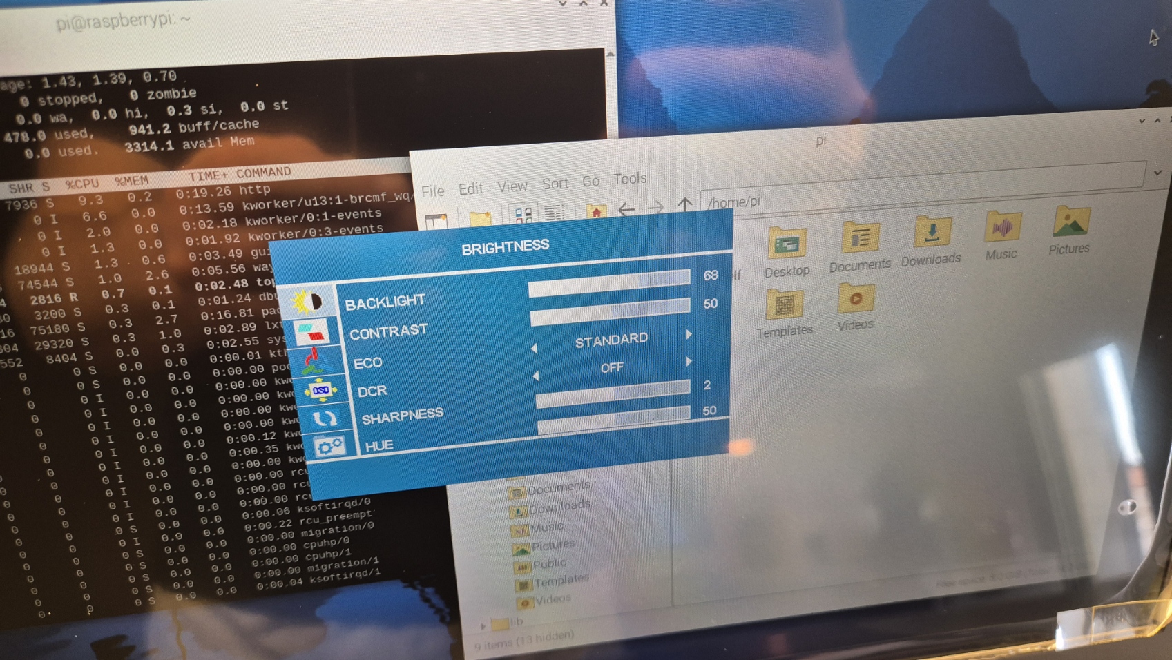
When it comes to performance, this device offers a reliable and smooth experience. The built-in 5000mAh battery provides 1-2 hours of operation without external power, which is convenient for short-term use on the go. Please note that no battery indicator is available. The battery can also charge devices like smartphones and power Raspberry Pi, making it super portable. The built-in speakers are good enough for casual listening and video calls, they offer satisfying sound quality for daily use. However, for a more immersive audio experience, users might prefer external speakers or headphones. Its keyboard shortcuts and On-Screen Display (OSD) settings enhance usability. Allowing users to easily adjust settings such as brightness, volume, and color temperature. The inclusion of multiple languages in the OSD menu caters to a global user base.
Getting Started
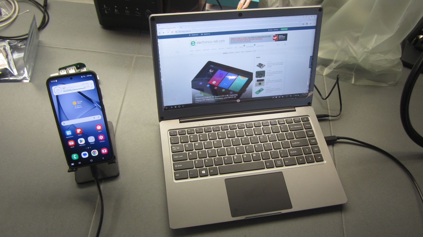
Setting up the CrowView Note -14” is straightforward, with clear instructions provided in the user manual. Connecting different devices is a hassle-free process, thanks to the variety of available ports and compatible cables (USB-A to USB-A, Type-C to Type-C, and HD to Mini HD). For specific devices like the Raspberry Pi 5 and Nvidia Jetson Nano Developer Kit, the CrowView Note requires additional Bridge Boards, which are sold separately. While this adds another step to the setup, it helps make sure everything works properly, it ensures optimal compatibility and performance for these specialized devices. This device works with different Operating Systems and platforms, which is why it is very good for people who use multiple OS for their work. Whether used as a secondary monitor for a laptop, a display terminal for a Mini PC, or an extension for a smartphone (supports Samsung DeX), this display adapts to different scenarios with ease.
Samsung DeX Mode Support
CrowView Note -14” supports Samsung DeX mode to enable a full-featured Android desktop computer on the go. To use this feature you will need a USB-C cable that supports video/data transmission along with power.
CrowView Note -14″ Specifications:
- Display:
- Size: 14 inches
- Resolution: 1920 x 1080 (FHD)
- Color Gamut: 100% sRGB
- Brightness: 300cd/m²
- Aspect Ratio: 16:9
- Battery:
- Capacity: 5000mAh, 7.4V
- Type: Built-in
- Operating Time: 1-2 hours without external power supply
- Power Output: Can power connected devices (e.g., smartphones, Raspberry Pi)
- Ports and Connectivity:
- 1 x USB-A (connect master device)
- 1 x USB-A (connect peripherals)
- 1 x Mini HD (signal transmission)
- 1 x Type-C (power supply, PD 5V/5A output)
- 1 x Type-C (full-featured, 5V/3A output)
- 1 x DC 3.5mm Interface (power supply, 12V/4A input)
- 1 x Headphone Jack
- Audio:
- Speakers: 2 x 8Ω/2W
- Input:
- Keyboard: Integrated
- Touchpad: Integrated
- OSD (On-Screen Display) Settings:
- Brightness: Adjustable range: 0-100
- Contrast: Adjustable range: 0-100
- ECO Mode: STANDARD/RTS/FPS/MOVIE/GAME/TEXT
- DCR: OFF/ON
- Sharpness: Adjustable range: 0-4
- Hue: Adjustable range: 0-100
- Saturation: Adjustable range: 0-100
- Color Temp: sRGB/USER/WARM/COOL (RGB adjustable in USER mode)
- Low Blue Light: Adjustable range: 0-4
- Volume: Adjustable range: 0-100
- Mute: OFF/ON
- Signal Source: Selectable
- Aspect Ratio: WIDE/4:3
- FreeSync: OFF/ON
- OD (OverDrive): OFF/ON
- Clone Mode: OFF/ON
- Compatibility:
- Compatible with devices having HD and Type-C (full-featured) interfaces
- Example devices:
- Smartphones: Huawei Mate series, Apple iPhone 15 series, Samsung Galaxy S and Note series
- Laptops: Apple MacBook series, Huawei MateBook series, Samsung Notebook series, Microsoft Surface Book 2, ASUS VivoBook and ROG series, Dell XPS and Alienware series, HP Pavilion and EliteBook series, Lenovo Legion and ThinkBook series
- Dimensions and weight:
- Size: 334 x 223 x 20 mm
- Weight: 1200g
- Additional Features:
- Status Indicator: White during operation
- Caps Lock Indicator: White when activated
- Num Lock Indicator: White when activated
- Microphone: Integrated
- Power Button: Short press to power on, long press to power off
- Power Indicator: Red during charging
Conclusion
The CrowView Note 14-inch is a fair-quality portable monitor that’s great for work, gaming, or watching videos. It connects easily to various sources using USB Type-C and Mini HDMI ports. It is lightweight and easy to set up and use for a bunch of different things and it is perfect for taking it with you wherever you go. You should keep in mind that this monitor doesn’t have a built-in computer, storage, or camera. Its design is very simple and convenient so you can add an extra screen to your devices or convert your smartphone to a laptop PC thanks to the remote desktop function of most modern devices.
The CrowView Note works with different devices and operating systems, so it’s a good choice for anyone looking for a portable second screen. This device is easy to use, and you can connect it to almost any device, reliably.
While the need for additional Bridge Boards for specific devices may be a minor inconvenience, the overall benefits and functionality of this device far outweigh this drawback. For those who are searching for a portable monitor that offers flexibility, durability, and excellent display quality, the CrowView Note 14″ is a highly recommended choice. Pricing information is not available at the time of writing this review.
For more information please visit the official site or the Kickstarter campaign.