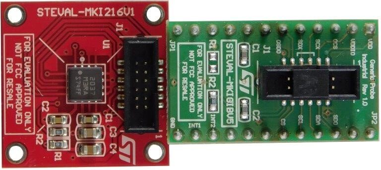
STMicroelectronics STEVAL-MKI216V1K Digital Inclinometer Kit combines an embedded IIS3DHHC 3D accelerometer sensor, which is connected via cable to a simple adapter board (STEVAL-MKIGIBV5) to render it compatible with STEVAL-MKI109V3 motherboards. The sensor is soldered precisely in the center of the board, and double-sided adhesives are provided to allowing the board to be mounted on equipment destined for vibration analysis. The STEVAL-MKIGIBV5 can be plugged into a standard DIL 24 socket.
The STM STEVAL-MKI109V3 Motherboards feature a high-performance 32-bit microcontroller functioning as a bridge between the sensor and a PC running the free Unico GUI graphical user interface or dedicated software routines for customized product summary applications.
Features
User friendly IIS3DHHC board
Complete IIS3DHHC pinout for a standard DIL 24 socket
Fully compatible with STEVAL-MKI109V3 motherboard
Double-sided adhesives included for easy mounting on equipment to be measured
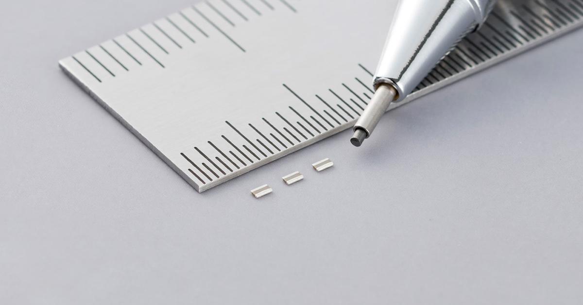
Murata’s Ultra-thin LW Reversed, Low ESL Chip MLCCs in 0204 inch Size Design for In-vehicle ADAS Applications
Murata introduces the ultra-thin LW reversed, low equivalent series inductor (ESL) multilayer ceramic capacitor (MLCC) with a capacitance value of 1.0 µF ±20% for 4 Vdc-rated automotive applications. With a 0204 inch size (0.5 x 1.0 mm) footprint and maximum thickness of just 0.22 mm, the LLC152D70G105ME01 decoupling capacitor can be implemented on the back of a processor package, contributing to lower impedance of a power supply line. It can also sit close to the main processor on the motherboard.
Compared to standard MLCCs, the LW reverse construction flips the electrodes through 90° so they are positioned on the long side of the rectangular chip. This change in construction reverses the length-to-width ratio, providing effective noise suppression in high-frequency applications.
As advanced driver-assistance systems (ADAS) continue to evolve to increase safety and, ultimately, deliver self-driving vehicles, ICs for in-vehicle equipment have become increasingly high-performance. To stabilize these ICs, more focus is being put on lowering the power supply lines’ impedance. Thanks to Murata’s proprietary thin layer technology for ceramic elements and thin-sheet formation technology, the LLC152D70G105ME01 LW reversed, low ESL chip MLCCs are effective for achieving a low-impedance design.
For more information about the LLC152D70G105ME01 LW reversed, low ESL chip MLCCs,
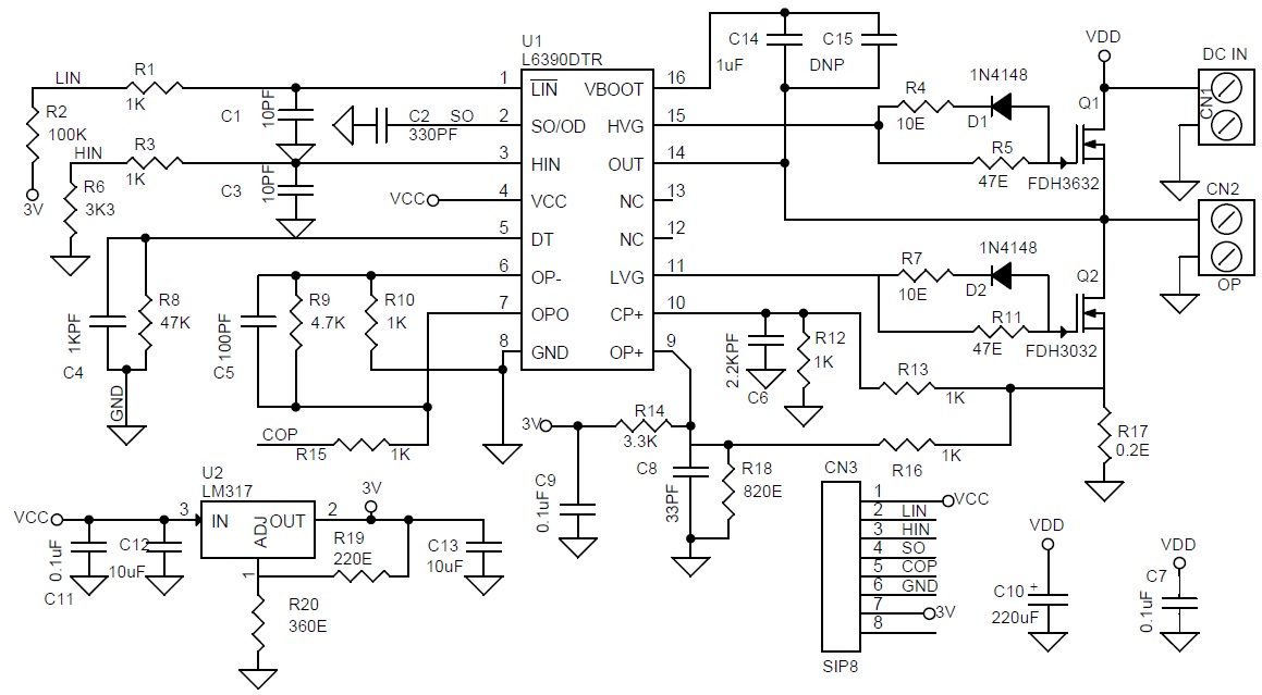
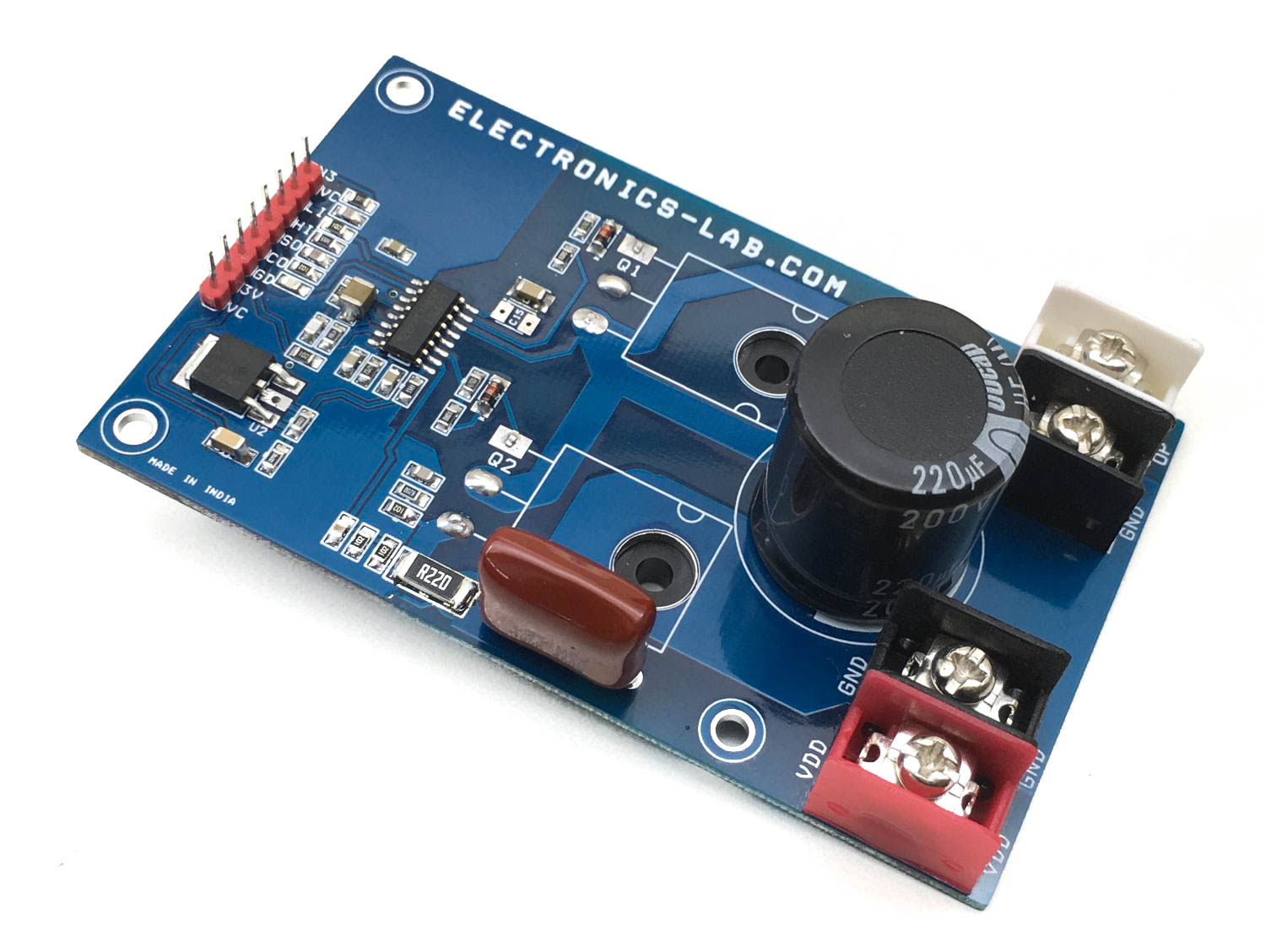
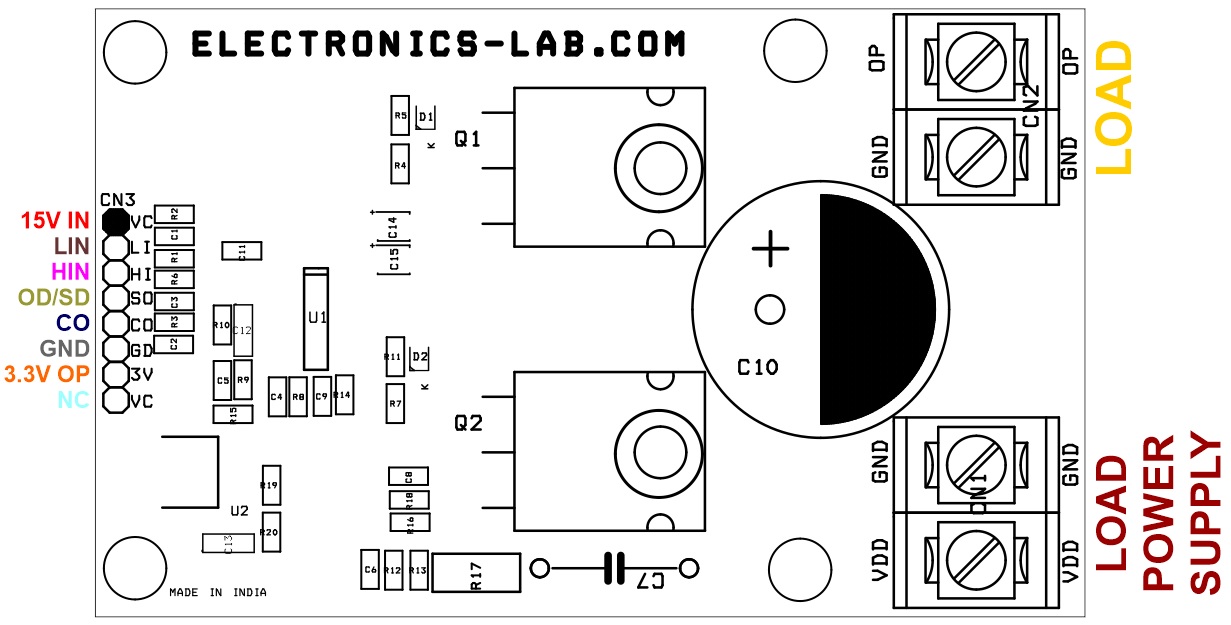
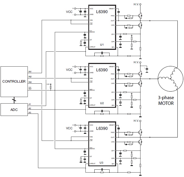
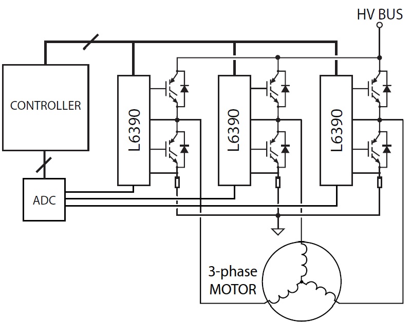
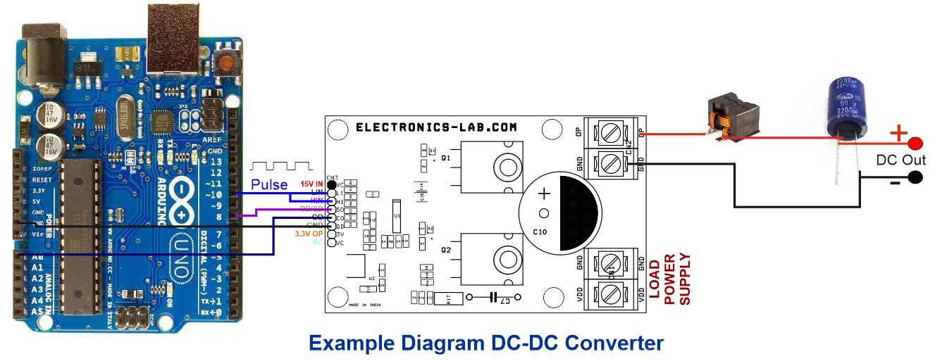
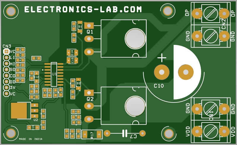
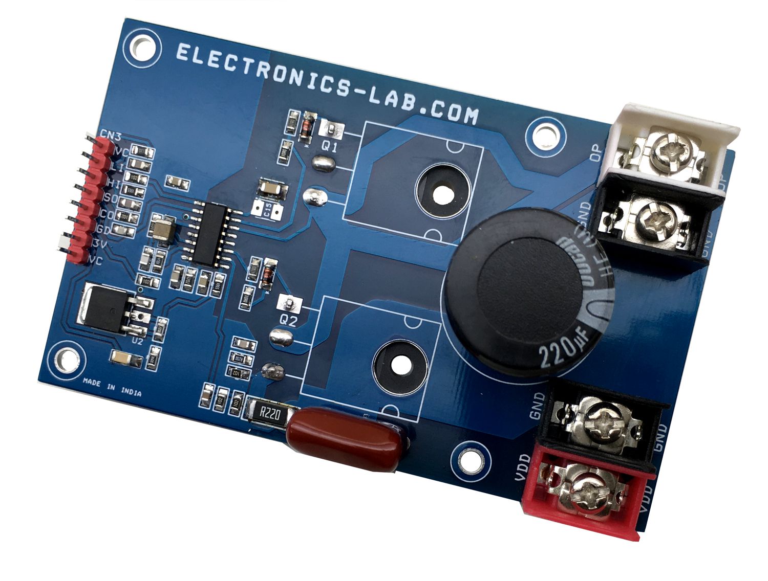
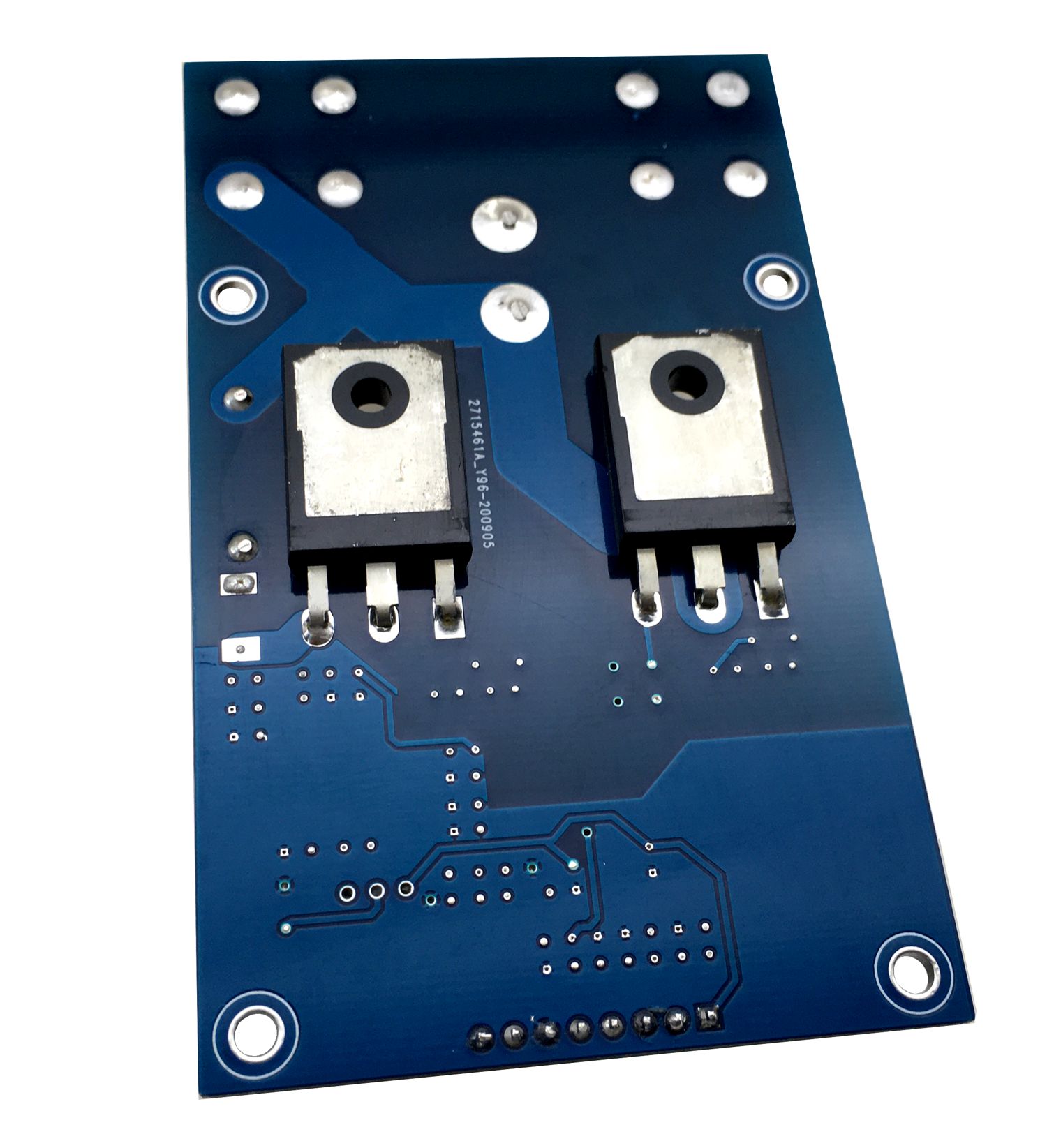
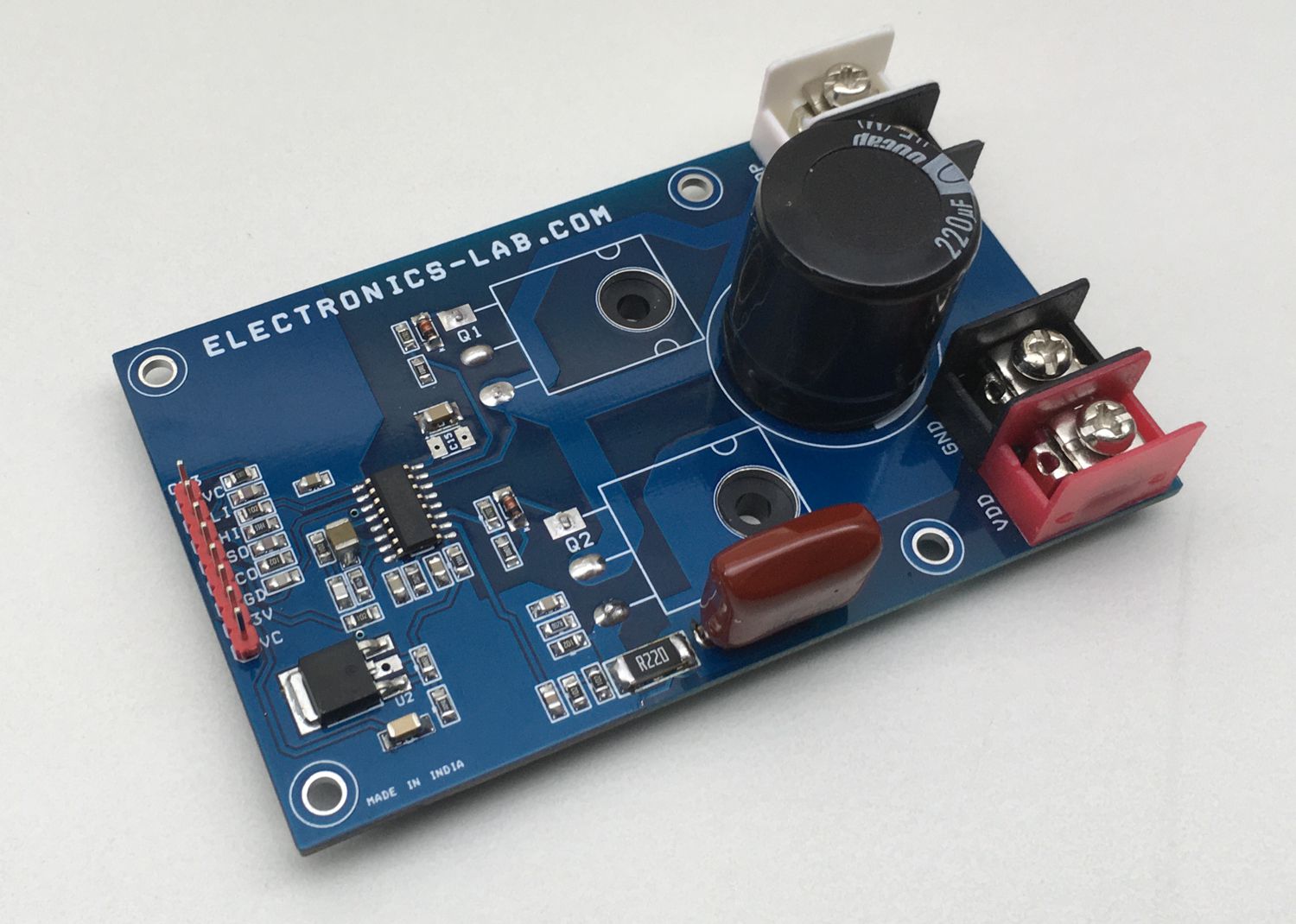
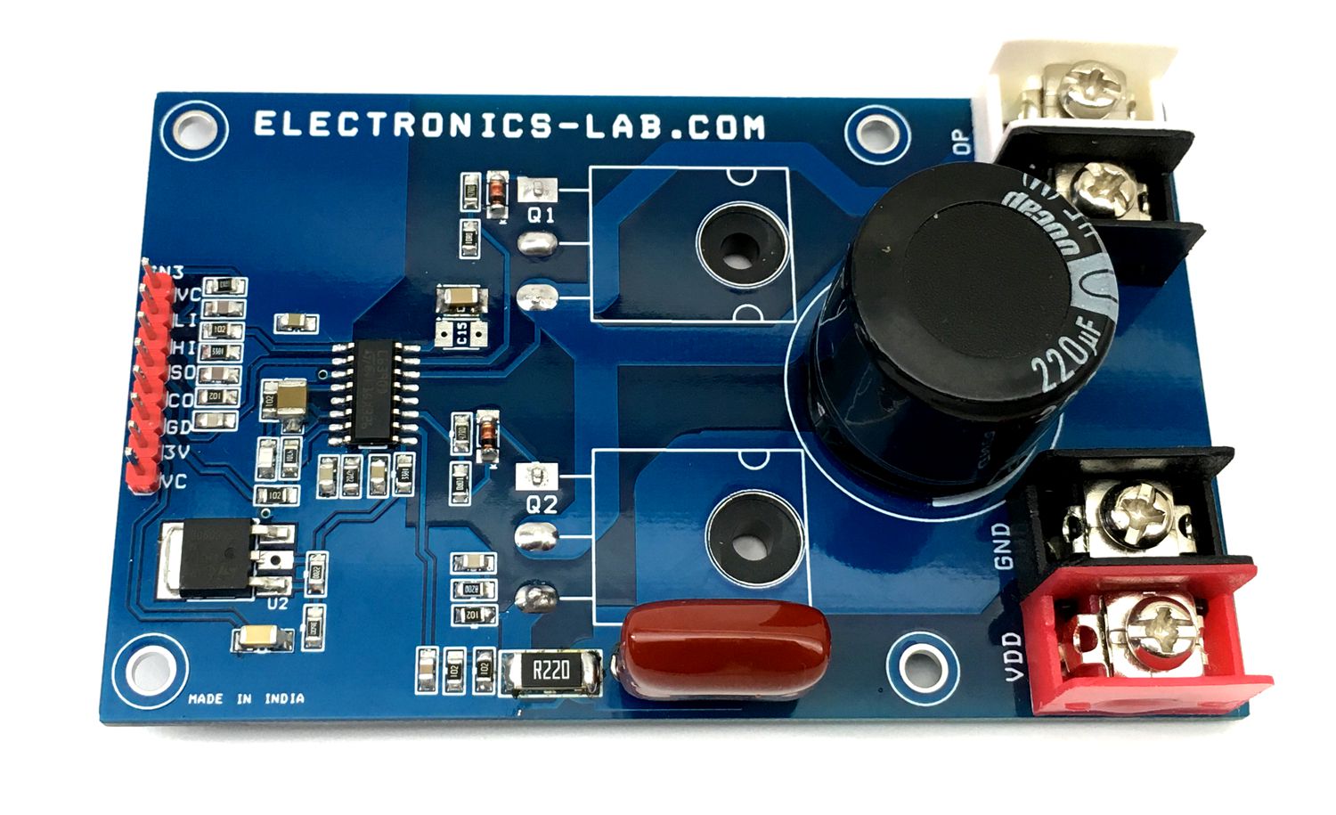
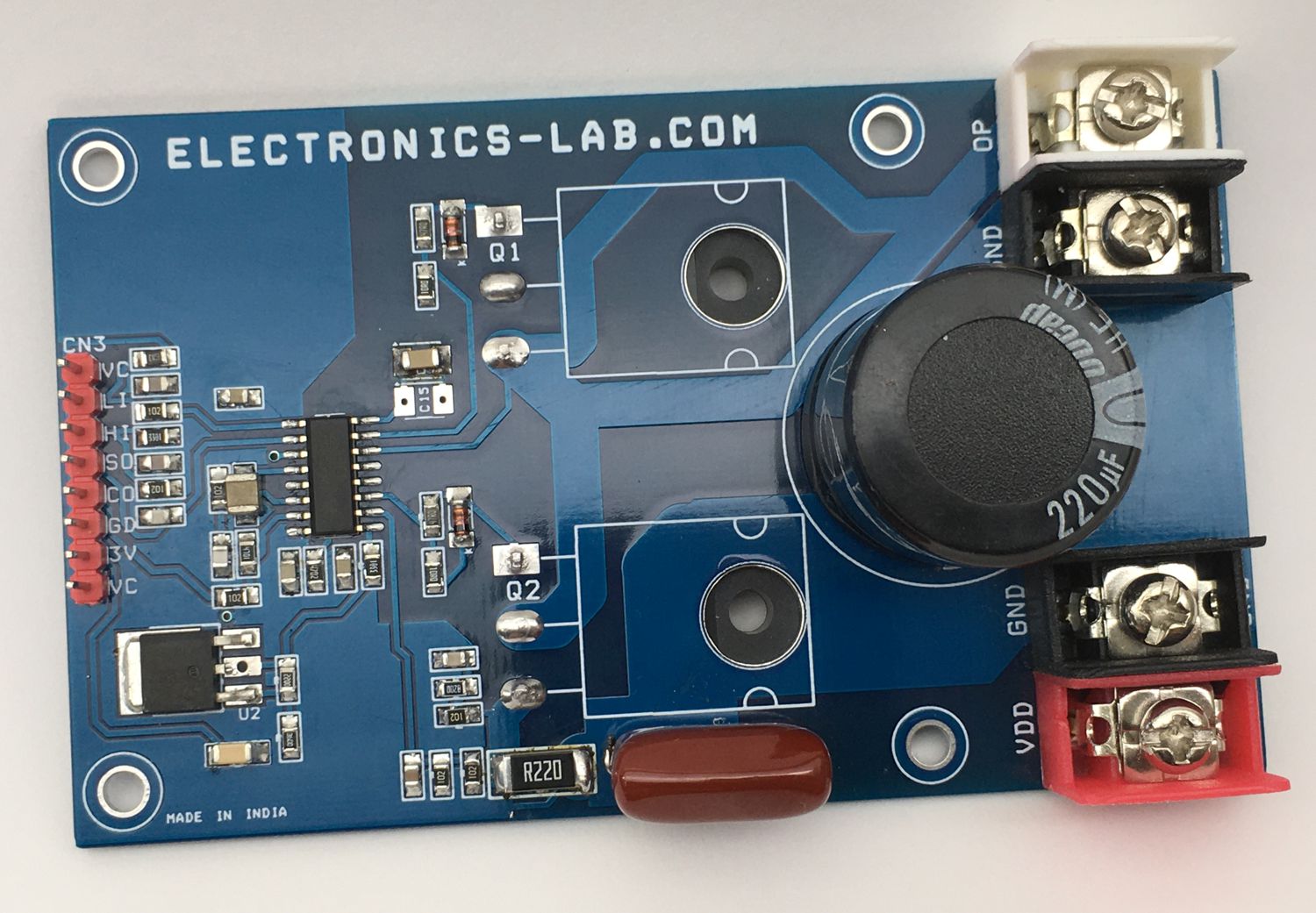
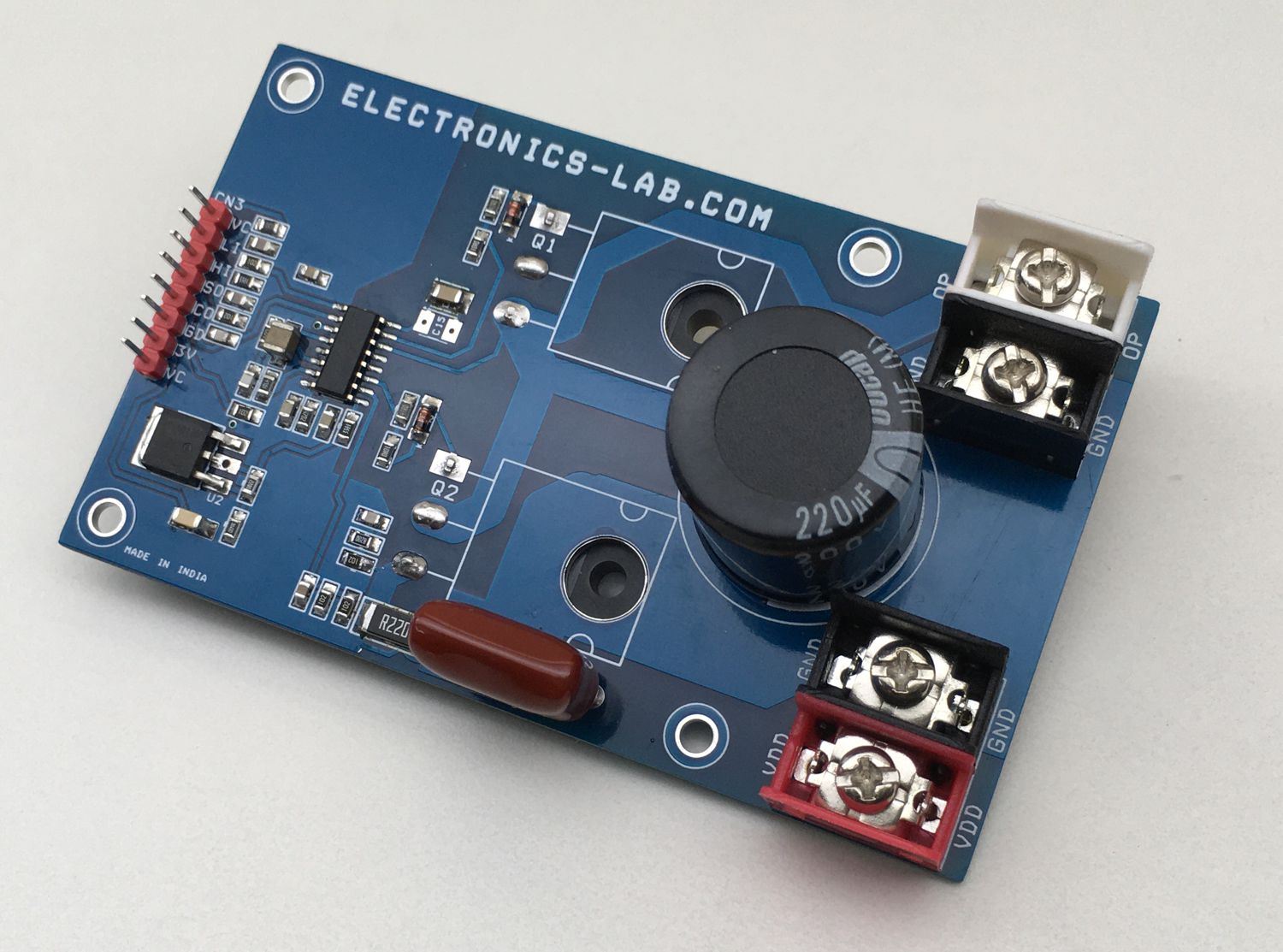
The project presented here is a versatile high voltage Half-Bridge with current feedback. The board is built using L6390 IC from ST Semiconductor. It is suitable for DC-DC converters, EHT drivers, induction heater drivers, battery chargers, LED drivers, DC motor speed controller and field-oriented control (FOC) motor driving application etc. The user can make a FOC Brushless motor driver with 3 of these units, Bidirectional Brushed DC motor can be controlled with 2 units. FDH3632 MOSFETs rated at 100V DC and 80A Current drive the output. Other High voltage and high current MOSFET can be used as per voltage and current requirements.
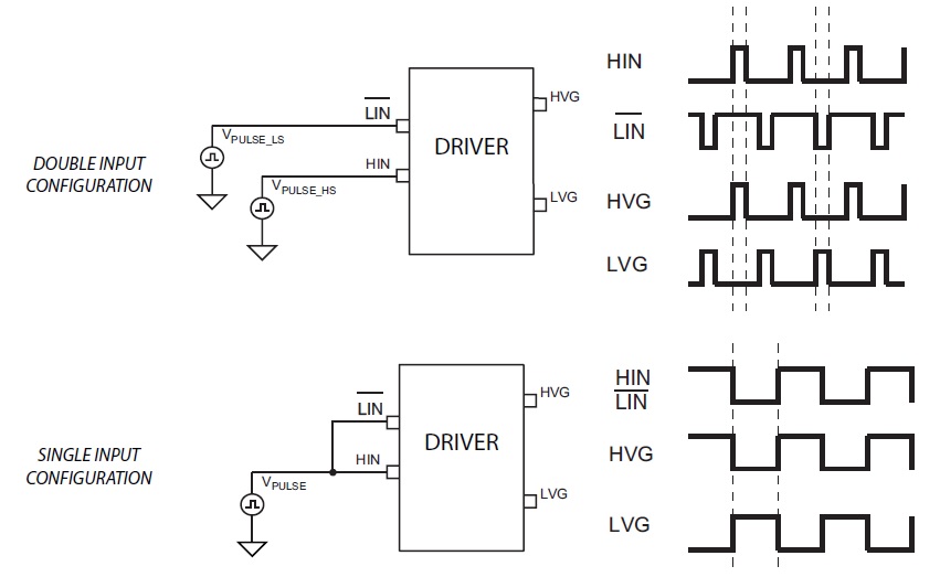
WeI have tested this board with 2A load and input frequency 10-80Khz. This project provides several more functions such as current feedback output, smart shutdown, fault shutdown etc. The board has two logic inputs, HIN and LIN, to separately control the high side and low side outputs, HVG and LVG. HIN is in phase with HVG, while LIN is out of phase with LVG. The signal inversion on the low side input allows control of the half-bridge output with only one control input signal. This board can work with double logic inputs or single input configuration. (See figure below for input configuration). Operating Load power supply 24V – 90V DC and logic supply 12-15V DC. U2 Regulator provides 3.3V DC output to drive Op-Amp circuitry and pull-ups. The board supports input signals 3.3V or 5V. Use large a size heatsink on MOSFETs for heat dissipation.
Features
Logic Power Supply VCC 12-15V DC
Load Power Supply VDD 24V-90V DC
Load 2 Amps (Change R17 Lower resistance and higher wattage for higher current Load)
Current Feedback Output 2.250V without Load + (0.5V/1Amp)
Inputs: HIN, 2.LIN, 3. Shutdown
Outputs: 1. Current Feedback 2. Fault Output
Input Signal HIN/LIN Frequency 10Khz – 80Khz Logic Level 3.3V/5V DC
LIN logic input: 720 kΩ (typ.) pull-up connected to an internal 5 V regulator through a diode, R2 100K External Pull up Resistor
SD logic input: 375 kΩ (typ.) pull-down, this pin required high logic input to enable the outputs. This pin goes low when fault condition occurs.
Note 1: I have used FDH3632 MOSFETs, hence maximum input load power supply is up to 90V DC
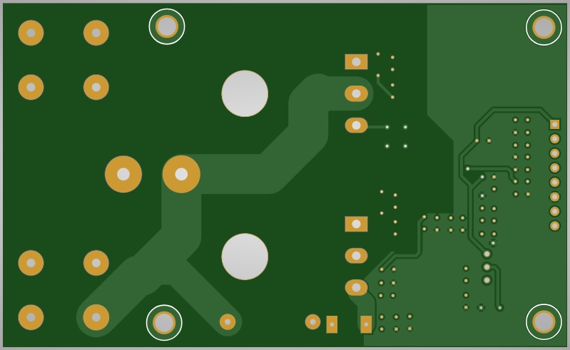
Note 2: This board can support higher voltage up to 400V DC, Choose appropriate MOSFETs, Capacitor C7, C10 for as per application requirements.
Note 3: I have tested this board with input frequency 10Khz to 80Khz, Project supports frequency up to 800Khz, choose C-Boot capacitor C14, C15 as per requirement.
Note 4: The board support 90V x 2A= 180W Power. Use Lower ohm/High Watt resistor R17 for Higher current requirement.
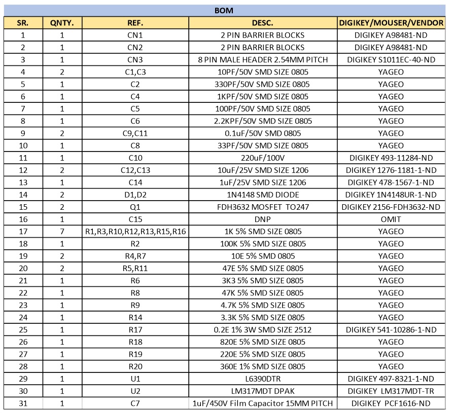
Input Connections CN3
Pin 1 : VCC 12V – 15 V DC Input Logic Supply /1Amp
Pin 2 : LIN Signal In
Pin 3 : HIN Signal In
Pin 4 : Enable In Pull High/Shutdown Out
Pin 5 : Current Feed Back Voltage Output
Pin 6 : GND
Pin 7 : 3.3V Output Max Load 100mA
Pin 8 : NC ( Not Connected)
Testing the board
Apply 12-15V DC to logic supply CN3 VC and GND)
Apply Load Supply 24 to 30V DC 3Amps to CN1
Connect the 10 Ohms Resistor at CN2 as load between output and GND
Tie (Shot)HIN/LIN pin and apply 20Khz Square wave Signal 3.3V/50V DC
Power on Both Power supply
Connect the S0 Pin to 3.3V/5V Power source with 10K Series resistor
L6390 High voltage high/ low-side driver
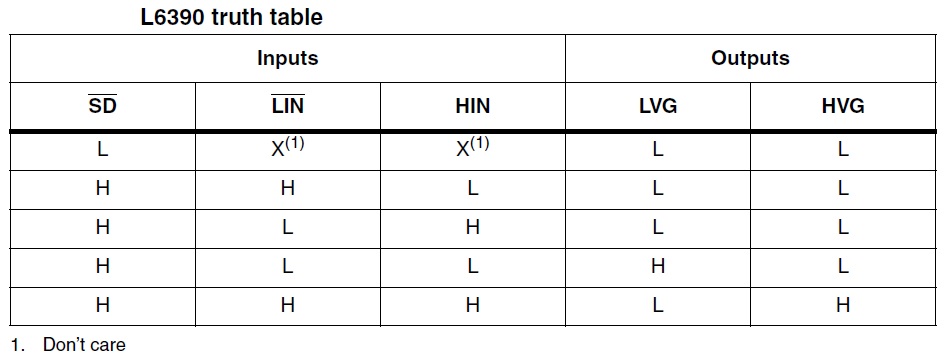
The L6390 is a high voltage half-bridge gate driver. This device can be used in all applications where high voltage shifted control is necessary. The devices have a driver current capability best suited for home appliance motor driving ratings, and they are also equipped with patented internal circuitry which replaces the external bootstrap diode. This feature is achieved by means of a high voltage DMOS synchronously driven with the low side gate driver. The L6390 is a half-bridge driver with several functions such as externally adjustable deadtime, interlocking, smart shutdown (patented), fault comparator and a dedicated high-performance op-amp for advanced current sensing. The outputs can be driven by two dedicated logic signals or, alternatively, only one logic signal by connecting the two inputs together. Device outputs can sink and source 430 mA and 290 mA respectively. Prevention from cross conduction is ensured by interlocking and programmable deadtime functions.
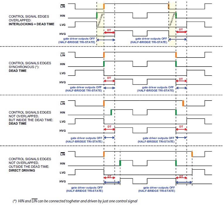
Dead Time: R8 provided to set the Dead time. The dead time can be set to a wide range of values from hundreds of nanoseconds to a few microseconds. In order to avoid any possible cross-conduction between the power MOSFETs/IGBTs of the half-bridge, the L6390 provides both the dead time and the interlocking functions. The interlocking function is a logic operation which sets both the outputs to low level when the inputs are simultaneously active (HIN to high level and LIN to low level). The dead time function is a safety time introduced by the device between the falling edge transition of one driver output and the rising edge of the other output. If the rising edge set externally by the user occurs before the end of this dead time, it is ignored and results delayed until the end of the dead time. The dead time can be adjusted externally through the value of the DT resistor R8 connected between pin 5 and GND. A capacitor C4 1 KPF ceramic capacitor in parallel with this resistor is provided for noise immunity. and interlocking function management are described.
Smart Shut-Down: The L6390 integrates a comparator for fault sensing purposes. The comparator has an internal reference voltage Vref on its inverting input (see L6390 datasheet), while the noninverting input is available on pin 10. The comparator input is connected to an external shunt resistor R17 in order to implement a simple over-current detection function. The output signal of the comparator is fed to an integrated MOSFET with the open drain available on pin 2, shared with the SD input. When the comparator triggers, the device is set in shutdown state and both its outputs are set to low level leading the half bridge in tri-state. In common over-current protection architectures, the comparator output is usually connected to the SD input and an RC network is connected to this SD/OD line in order to provide a mono-stable circuit, which implements a protection time that follows the fault condition. Unlike common fault detection systems, the L6390 smart shutdown architecture allows to immediately turn-off the output gate driver in case of fault, by minimizing the propagation delay between the fault detection event and the actual outputs switch-off. In fact, the time delay between the fault and the outputs turn-off is no more dependent on the RC value of the external network connected to the pin. In the smart shutdown circuitry, the fault signal has a preferential path which directly switches off the outputs after the comparator triggering. At the same time the internal logic turns on the open drain output and holds it on until the SD voltage goes below the SD logic input lower threshold. The smart SD system provides the possibility to increase the time constant of the external RC network (that is the disable time after the fault event) without increasing the delay time of the protection. Any external signal provided to the SD pin is not latched and can be used as control signal in order to perform, for instance, PWM chopping through this pin. In fact, when a PWM signal is applied to the SD input and the logic inputs of the gate driver are stable, the outputs switch from the low level to the state defined by the logic inputs and vice-versa.
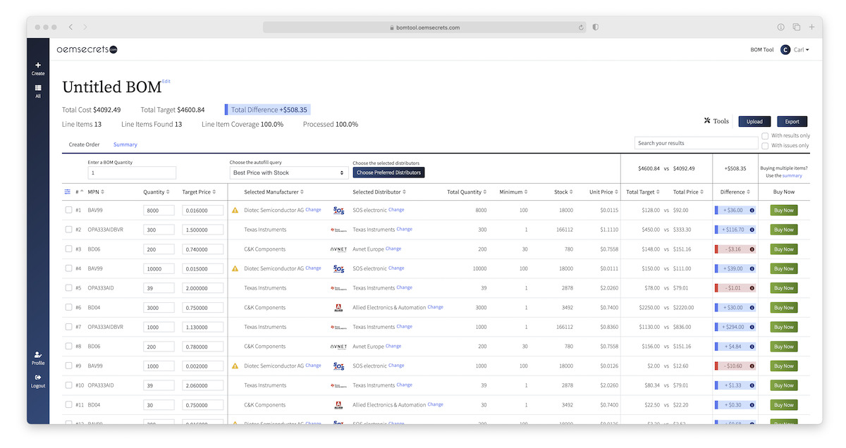
The oemsecrets.com BOM Tool creates a simple way to upload a list of parts and get the best price (with customizable options) for each line with a link to purchase from each distributor. Access to the Tool will allow you to upload BOMs up to 250 line items. oemsecrets.com compares distributor pricing and inventory for electronic parts. Register now for free.
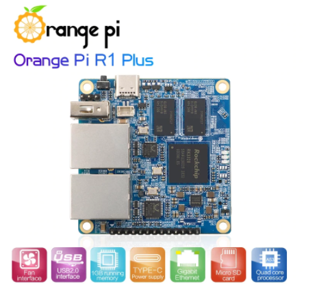
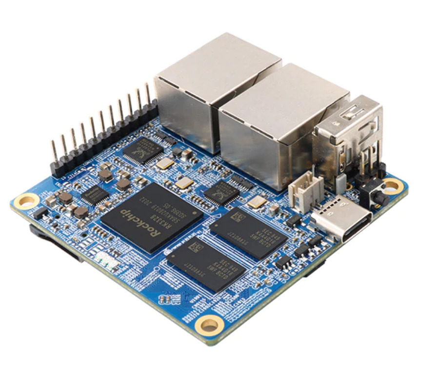
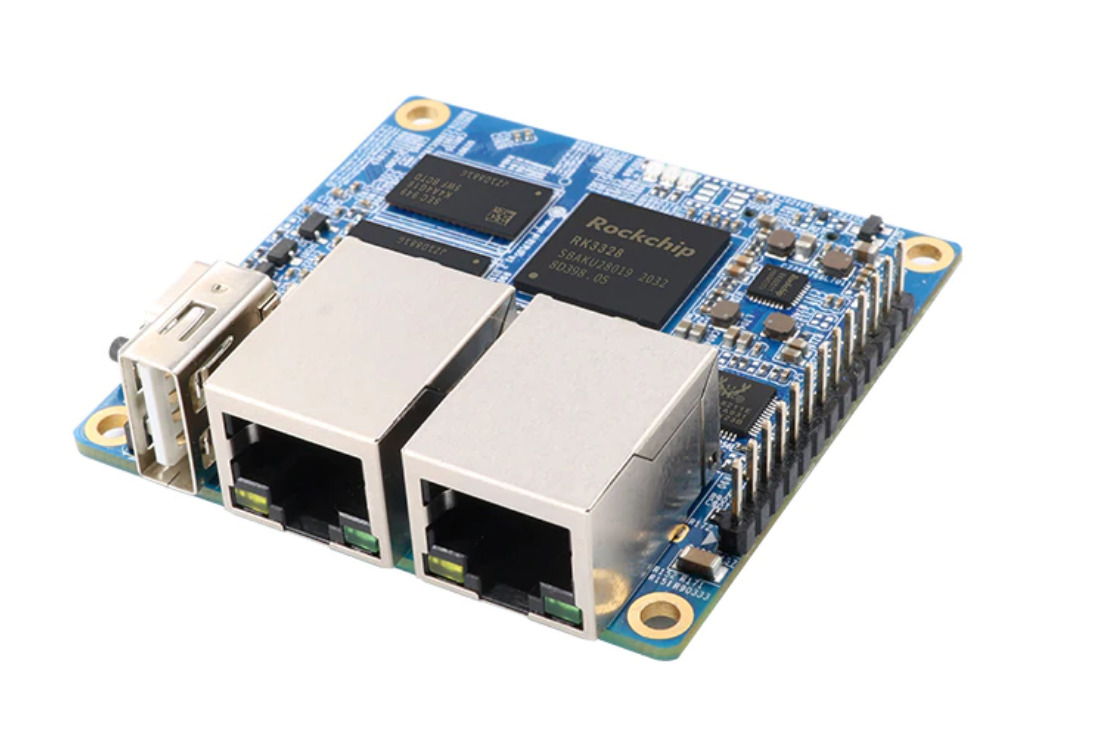
We have covered some interesting Orange Pi boards in the past. An example of it is the Orange Pi Zero 2. The main take away is that the name is one of the only things they have in common. With the Orange Pi R1 plus, the conversation goes to another path, as you really cannot compare some of its features with any other Raspberry Pi. Today, we will dig into it and see what unique there is about it.
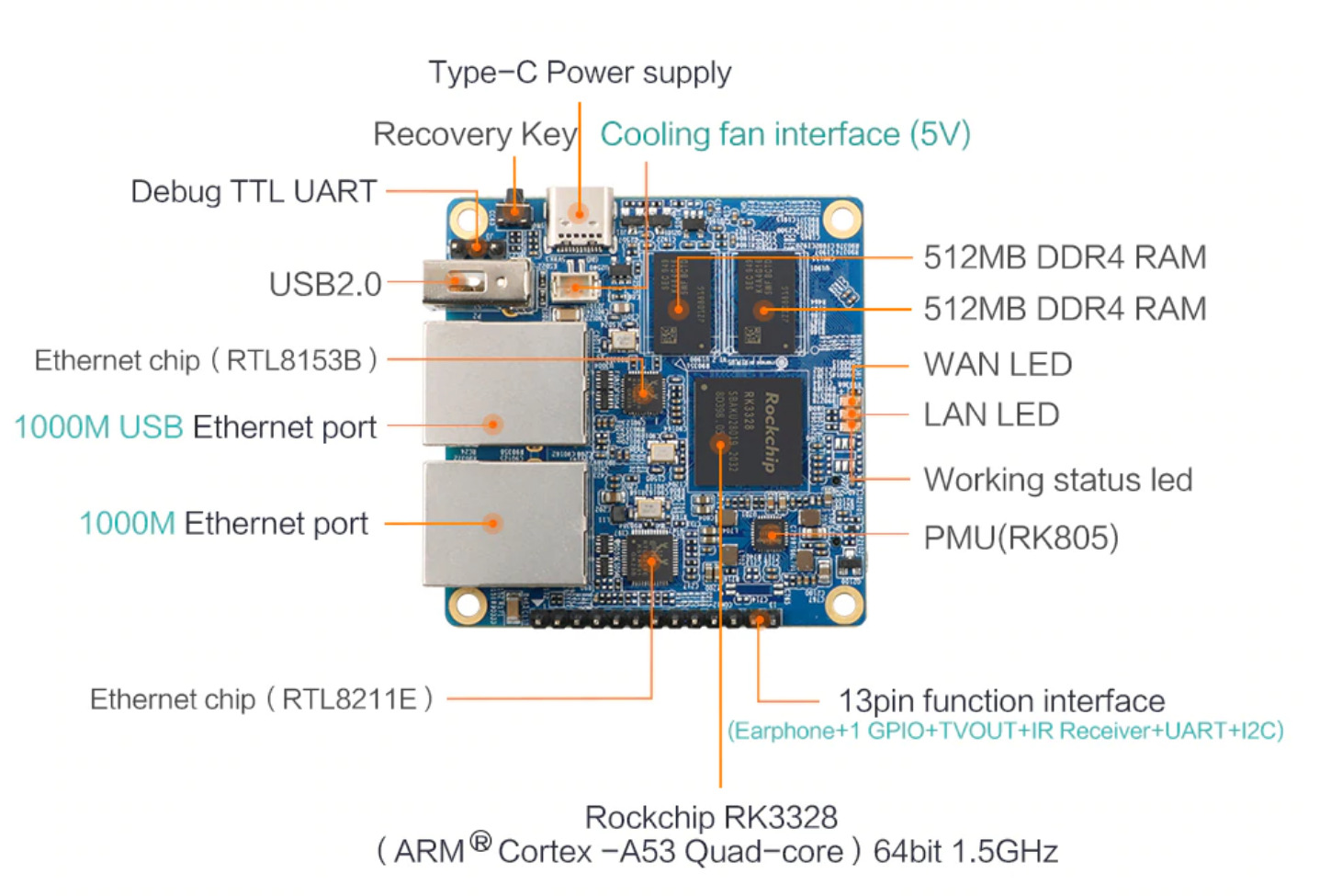
So, the new Orange Pi R1 Plus SBC is the new addition to the Orange Pi family, and can be compared with its partner Orange Pi R1. At first glance, they look quite different, and they actually are, as pretty much everything gets a considerable upgrade, starting with the SoC, the memory and the Ethernet. But not everything is great, as you are leaving some useful functionalities such as Wi-Fi behind with this new version.
Now, looking at both of them side by side (Orange Pi R1 in parentheses for some of the most important specs):
Rockchip RK3328 64-bit SoC – Quad-core ARM Cortex-A53 clocked at 1.5 GHz (Allwinner H2+ 32-bit SoC with ARM Cortex-A7, clocked at 1.2GHz)
ARM Mali 450 MP2 GPU with support for OpenGL ES 1.0 / 2.0 (ARM Mali 400 MP2 GPU)
Connectivity: 10M / 100M / 1000M ethernet (10M / 100M ethernet and Wi-Fi) and USB ethernet
TV CVBS video output, 3.5 mm audio port (via 13 pin interface board) and 1x USB 2.0 HOST port
Low level peripherals: 13 pin header with IR pin, TV output, audio (no microphone), 2x USB 2.0 and 1 GPIO port
1x Reset button, 1x cooling fan interface, power and status LED’s
Power: USB Type-C – 5 V / 2 A input (Micro USB)
Support for Android 9, Ubuntu, Debian and OpenWRT OS’s (Android 4.4, Lubuntu, Debian and Armbian Image)
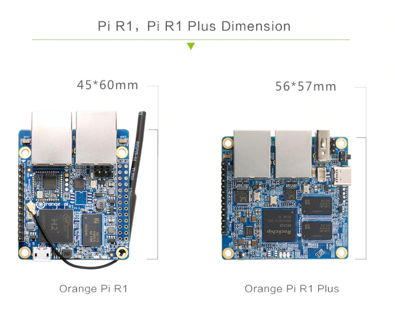
Dimensions of 56 mm x 57 mm (45 mm × 60 mm) and weight of 30.5 grams (35 grams)
Both Orange Pi R1’s side-by-side
As you can see, the “Plus” added to the name sort of undermines the very considerable upgrade the Orange Pi R1 Plus is when side-by-sided with its predecessor. Now, the absence Wi-Fi is a blow, and I think they acted wrong in ditching it, because we highly depend on it nowadays. But, aside from that step in the wrong direction, there is really not much to point my finger into. They provided a much needed upgrade here.
Now, the board is cool and all, but where do I use it? Easy, from an infotainment system to a wireless server, taking advantage of the ethernet, you can do pretty much anything. Lastly, let us discuss the pricing: coming at $24.99, it should be something to consider.
ESP32-S2-MINI-1 is a powerful, generic Wi-Fi MCU module that has a rich set of peripherals
ESP32-S2-MINI-1 is a powerful, generic Wi-Fi MCU module that has a rich set of peripherals. This module is an ideal choice for a wide variety of application scenarios relating to the Internet of Things (IoT), wearable electronics, and smart home.
At the core of this module is ESP32-S2, an Xtensa® 32-bit LX7 CPU that operates at up to 240 MHz. ESP32-S2 integrates a rich set of peripherals, including SPI, I2S, UART, I2C, LED PWM, ADC, DAC, touch sensor, temperature sensor, and up to 43 GPIOs. It also includes a full-speed USB On-The-Go (OTG) interface to enable USB communication.
Key features
Unparalleled security for your connected devices
Helps you build connected low-power devices
Build whatever you like with its rich IO capabilities
Cost-effective
Additional features
MCU
Embedded ESP32-S2, with Xtensa® single-core 32-bit LX7 microprocessor, up to 240 MHz
128 KB ROM
320 KB SRAM
16 KB SRAM in RTC
Hardware
Interfaces: GPIO, SPI, LCD, UART, I2C, I2S, Camera interface, IR, pulse counter, LED PWM, USB OTG 1.1, ADC, DAC, touch sensor, temperature sensor
The 3W 3535 Surface Mount UV LEDs are energy-efficient LEDs that can be driven using high currents and can dissipate heat efficiently
The 3W 3535 Surface Mount UV LEDs are energy-efficient LEDs that can be driven using high currents and can dissipate heat efficiently, resulting in higher reliability. Their low-profile package design addresses a wide variety of applications where superior robustness and high efficiency are required. They are packaged with ceramic-based materials, and the quartz lens on top of the package provides the product longevity needed for the respective end applications. To facilitate easy pick & place assembly, the LEDs are packed in tape and reel. Each reel is shipped in a single flux and single color bin to ensure close uniformity.
Key features
High-reliability package with quartz encapsulation
High-radiant flux output using InGaN dice technolog
Available in 360-nm to 400-nm wavelength range
Available in 35° and 60° viewing angles
Additional features
Lens material: quartz
Terminals finish: gold plated
Electrically isolated thermal pad
Manufacturing technology: InGaN
Absolute max. power: 4000 mW (2800 mW for 360-nm devices)
Absolute max. forward current: 1000 ma (700 mA for 360-nm devices)
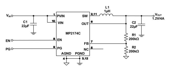
MPS’ MP2174C is a 2.7 V to 5.5 V, 4 A, high-efficiency, synchronous step-down converter
Monolithic Power Systems’ MP2174C is a monolithic, step-down, switch-mode converter with built-in, internal power MOSFETs. It achieves 4 A of continuous output current from a 2.7 V to 5.5 V input voltage with excellent load and line regulation. The output voltage can be regulated as low as 0.6 V. The device has a constant on-time (COT) control scheme providing fast transient response and easy loop stabilization. Fault condition protections include cycle-by-cycle current limit and thermal shutdown. The MP2174C requires a minimal number of readily available standard external components. It is available in an ultra-small QFN-12 (2 mm x 2 mm) package making it ideal for a wide range of applications, including PDAs, portable instruments, DVD drives, and handheld devices.
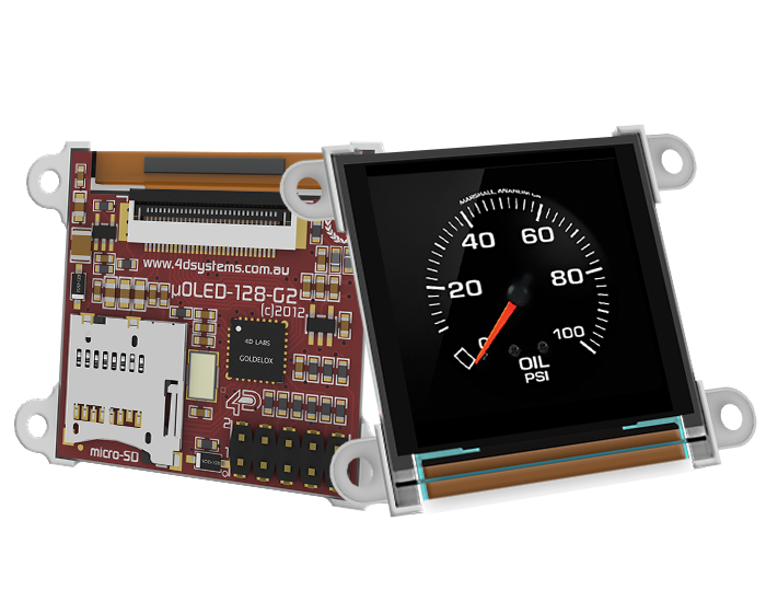
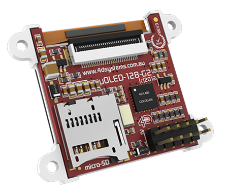
The uOLED-128G2 is a compact and cost effective display module using the latest state of the art Passive Matrix OLED (PMOLED) technology with an embedded GOLDELOX graphics processor that delivers ‘stand-alone’ functionality to any project.
Powerful graphics, text, image, animation and countless more features are built inside the GOLDELOX chip. The module is designed to work out of the box and you are now ready to write your code in 4DGL (a high level 4D Graphics Language) using the 4DGL-Workshop4 IDE (editor, compiler and downloader). This will save weeks even months of development time on your next embedded graphics project.
4DGL is a graphics oriented language allowing the developer to write applications in a high level language, syntax similar to popular languages such as BASIC, C and Pascal. The module offers modest but comprehensive I/O features that can interface to serial, analogue, digital, buttons, joystick, sound generation and Dallas 1-wire devices.
Information about the display module
Low-cost OLED display graphics user interface solution.
128 x 128 resolution, 65K true to life colours, PMOLED screen.
1.5″ diagonal size Active Area on the OLED Display.
No back lighting with near 180° viewing angle.
Easy 10 pin interface to any external device:
VCC, TX, RX, GND, RESET, IO1, IO2, 3.3V.
Powered by the 4D-Labs GOLDELOX graphics processor highly optimised for 4DGL, the high level 4D Graphics Language.
2 x GPIO ports supports:
Digital I/O
A/D converter with 8/10 bit resolution
Complex sound generation
Dedicated RTTTL tune engine
Multi-Switch Joystick
Dallas 1-Wire
10K bytes of flash memory for user code storage and 510 bytes of RAM for user variables (255 x 16bit vars).
1 x Asynchronous hardware serial port, TTL interface, with 300 baud to 600K baud.
On-board micro-SD memory card adaptor for storing of icons, images, animations, etc. Supports 64MB to 2GB micro-SD memory cards.A SPI compatible micro-SD card is required.
Comprehensive set of built in high level 4DGL graphics functions and algorithms that can draw lines, circles, text, and much more.
Display full colour images, animations, icons and video clips.
Supports all available Windows fonts and characters (imported as external fonts).
4.0V to 5.5V range operation (single supply).
Module dimensions: 36 x 36 x 13.7mm (including corner plates).
Weighing ~10g.
Display Viewing Area: 27 x 27mm
Back plate with 4 x 3mm holes for mechanical mounting.
RoHS Compliant.
CE Compliant (On Modules with CE Mark).
This module can be programmed using 3 different environments in the Workshop4 IDE. Designer, ViSi and Serial. Please refer to the Workshop4 Product Page for more information and documentation on these environments.
In short, the uOLED-128G2 offers one of the most flexible embedded graphics solutions available.
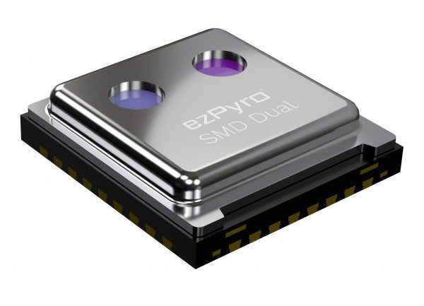
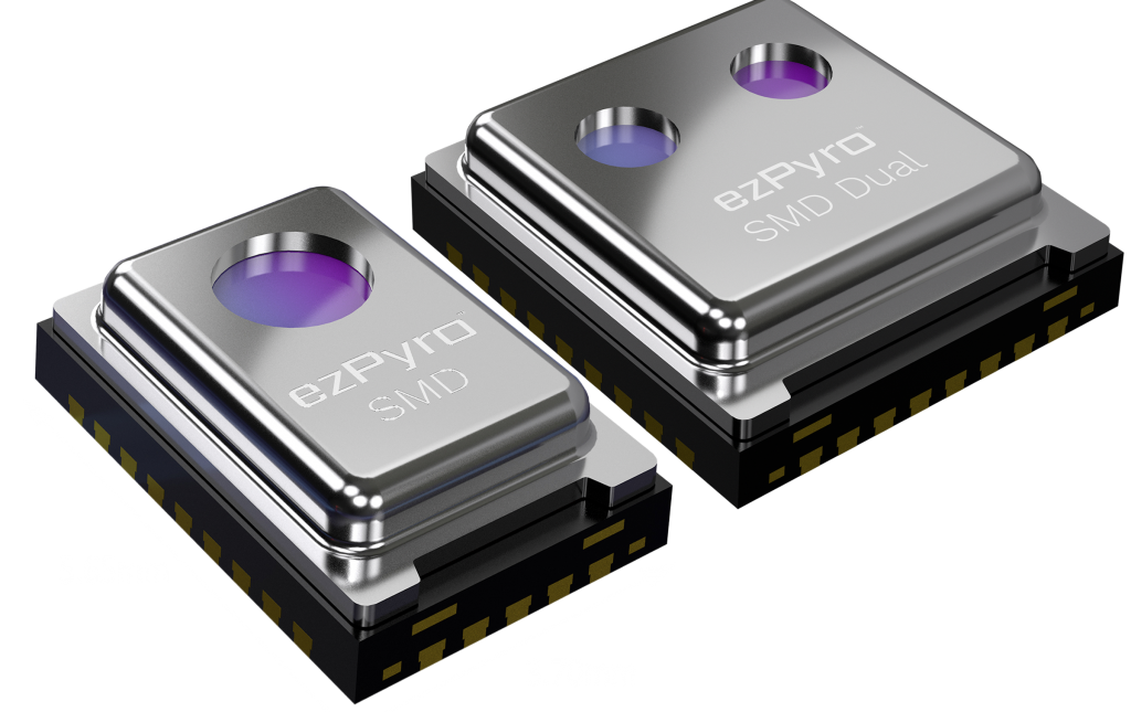
Pyreos has confirmed that its ezPyro SMD Dual is shipping in prototype form for a new wider range of substances, and benefits from all software and hardware components of the established Pyreos development ecosystem.
Part of the world’s smallest and fastest family of pyroelectric sensors, the ezPyro SMD Dual collocates two thin-film PZT pyroelectric elements separated by just 1.6 mm Inter-Pixel Distance (IPD). The small IPD means that two channels can be measured by illuminating an area just 2.8mm across, making for an optically simple and energy-efficient design.
As well as being physically smaller, ezPyro reduces costs in several ways; the digital readout reduces system component count/cost and the integration of two channels further reduces cost and space. The lower Inter-Pixel Distance and reduced component count enables a physically smaller design which further saves solution cost and energy demand.
ezPyro SMD Dual now has a widened range of gas detection options. The dual-channel sensor solution can detect carbon dioxide (CO2), methane (CH4) and hydrocarbons, refrigerants, nitrogen oxides (NOx), and sulphur oxides (SOx). Besides more expansive gas sensing it is ideal for analysis of foods including fats, sugars, proteins, alcohol and acidity.
The ezPyro SMD Dual combines high sensitivity with benefits such as low power consumption, built-in power management, a digital interface with plug-and-play connectivity to microcontrollers, and the cost-effectiveness of SMD design. Compatible with the complete ezPyro evaluation and development ecosystem, ezPyro SMD Dual shares the integrated read-out circuitry and an I2C digital communications bus. This integrated system ensures that it is very quick and easy for customers to develop into their product designs.
The fast development cycle of the ezPyro sensor family is supported by evaluation kits for flame, gas, motion and gesture detection. Other applications can be trialled using the ezPyro SMD prototyping system which supports up to four sensor breakout boards. Sensor evaluation without any software development effort is enabled by Pyreos PC software.
ezPyro is suitable for low power applications with a current consumption below 50µA when fully activated and less than 1µA in the lowest power mode.
“By extending our industry-leading dual-channel ezPyro SMD pyroelectric sensor, we deliver greater flexibility and choice to our customers,” said Andrew Wallace, CEO at Pyreos. “Compared to alternative pyroelectric and thermopile sensors, the ezPyro range offers higher sensitivity, faster response and switch-on, lower power consumption, more on-the-fly configurability, lower component counts and easier integration. Our unique technology allows inter-pixel gaps of around ten microns and this product is one more step towards even smaller detectors.”