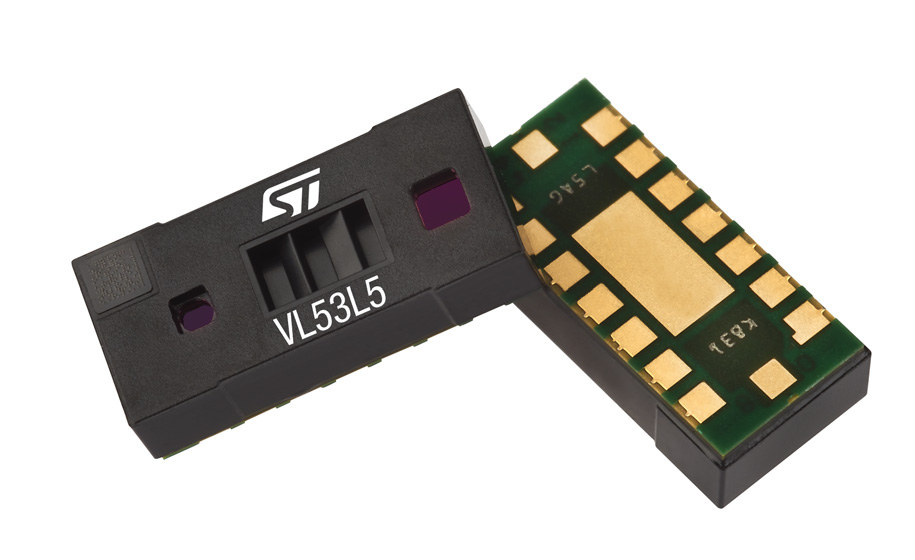
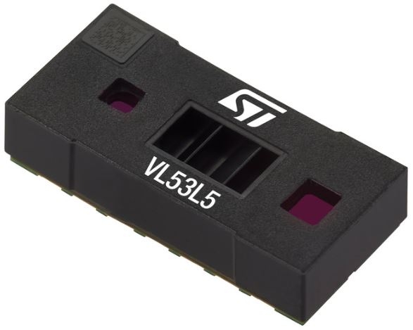
The VL53L5 is a state of the art, Time-of-Flight (ToF), laser-ranging sensor enhancing the ST FlightSense product family. Housed in a miniature reflowable package, it integrates a SPAD array, physical infrared filters, and diffractive optics (DOE) to achieve the best ranging performance in various ambient lighting conditions with a range of cover glass materials.
The use of a DOE above the vertical cavity surface emitting laser (VCSEL) allows a square FoV to be projected onto the scene. The reflection of this light is focused by the receiver lens onto a SPAD array. Unlike conventional IR sensors, the VL53L5 uses ST’s latest generation, direct ToF technology which allows absolute distance measurement whatever the target color and reflectance. It provides accurate ranging up to 400 cm and can work at fast speeds (60 Hz), which makes it the fastest, multi-point, miniature ToF sensor on the market.
Key Features
Fully integrated miniature module
Emitter: 940 nm invisible vertical cavity surface emitting laser (VCSEL) and integrated analog driver
61 ° diagonal square system field of view (FoV) using diffractive optical elements (DOE) on both transmitter and receiver
Receiving array of single photon avalanche diodes (SPADs)
Low-power microcontroller running Firmware
Size: 6.4 x 3.0 x 1.5 mm
Fast, accurate distance ranging
Parallel multi zone output; either 4×4 or 8×8 separate regions of interest (ROI)
Up to 400 cm ranging
60 Hz frame rate capability
Histogram processing and algorithmic compensation minimizes or removes impact of cover glass crosstalk
Dynamic crosstalk compensation for fingerprint smudge via latest patented ToF techniques
Easy integration
Single reflowable component
Flexible power supply options, single 3.3 V or 2.8 V operation or combination of either 3.3 V or 2.8 V AVDD with 1.8 V IOVDD
Compatible with wide range of cover glass materials
I²C or SPI interface
Low-power pin and two general purpose inputs (GPIOs) for interrupt and synchronization
Full set of software drivers (Linux and Android compatible) for turnkey ranging
With patented algorithms and ingenious module construction, the VL53L5 is also able to detect different objects within the FoV with depth information at 60 Hz. Scene browsing and multi zone detection is possible with the VL53L5 thanks to a software customizable detection array to achieve a quicker touch-to-focus or mini depth map.
Nowadays, technology is more and more used as a means to understand our bodies and provide us with some extra quality when it comes to our health. At the epicenter of this are the IoT devices that we use everyday, such as our smartwatches, that give us many interesting insights on the physical activities that we endure, monitors our sleep and even helps in staying healty, reminding us to drink water, get up, among other things. Besides that, the acquisition of data regarding the human body can help in further advancing the health field. But there is a small caveat: the platforms and sensors use are costly, making some people stay away from these sorts of projects, like us, hobbyists. Imagine the things we can do with a cheap and reliable bio-signals sensing platform. Now, think E3K!
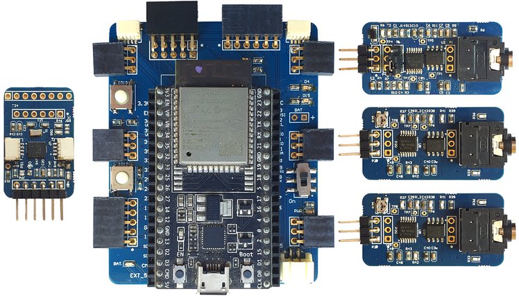
Let me explain: E3K is a bio-signals platform that aggegates computing power, Bluetooth Low Energy and Wi-Fi connectivity along with bio-sensors. By their words, their aim is “providing an affordable, fully open-source, wireless framework for an intuitive understanding of bio-signals originated from the human heart, muscle, and brain”. It counts with a electromyography sensor (EMG), for muscle movements, a electrocardiography sensor (ECG), for the heart signals, a electroencephalography sensor (EEG), to capture brain activity and a 9-DOF Inertial Measurement Unit (IMU), to sense motion. Besides that, it combines them in a kit that enables you to take advantage of them at a high sample rate and connect whatever else you deem necessary for your application. As simple as Plug-N-Play, but you have some degree of freedom when it comes to customization, which is very interesting to see.
Regarding specifications, here is what you can expect from this development kit, besides the sensors:
Based on ESP32 development kit
Peripherals: 1x I2C port, to use the IMU sensor, 6x 3-pin headers to use with analog sensors (12-bit resolution) to use the EMG and ECG/EEG modules, 1x 5-pin header with 3 analog pins, to use the EMG and ECG/EEG sensors, 2x Qwiic I2C connectors, 1x SPI port, all ESP32 Dev kit pins, 2x 8-Bit DAC
Connectivity: Wi-Fi, Bluetooth 4.2 with BR/EDR and BLE and USB 2.0
On-board accelerometer, gyroscope and triaxial geomagnetic sensor
2x LEDs and buttons
Powered via USB of LiPo battery (with on-board charging and standard battery connector), with voltage ranging from 3.3 to 6 V
Sampling rate from 1 to 2000 Hz
Custom, open-source GUI for data acquisition
Programmable via Arduino IDE and Espressif IDF, with Arduino libraries and Python APIs being under development
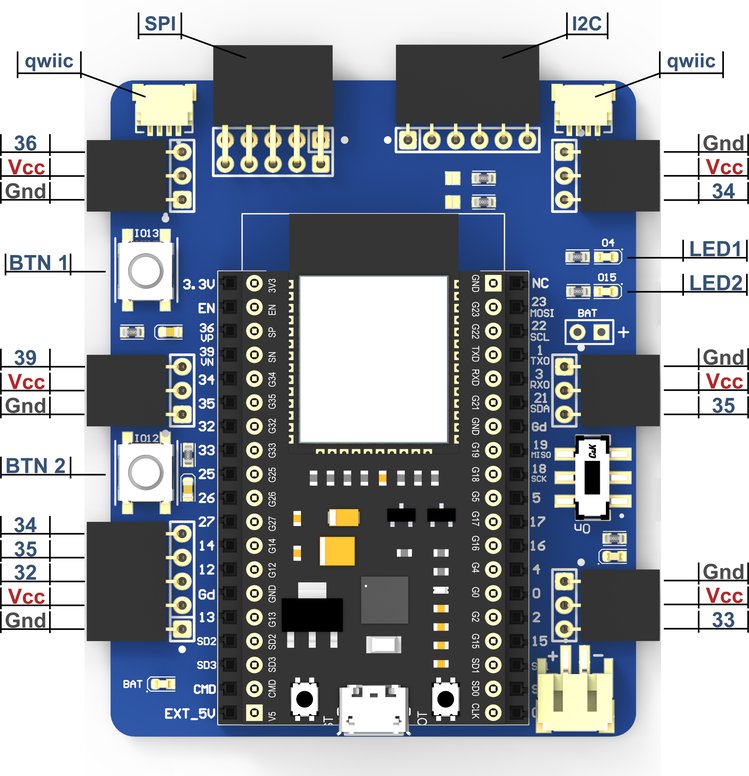
Pinout of the data communication and processing unit
From such a solid development kit, you are probably expecting it to be expensive, but on reality, it really is not. You can get the combo for a mere $159 in CrowdSupply. Lastly, if you want to help them out, they are currently in the middle of funding, with still 22 days left to go.
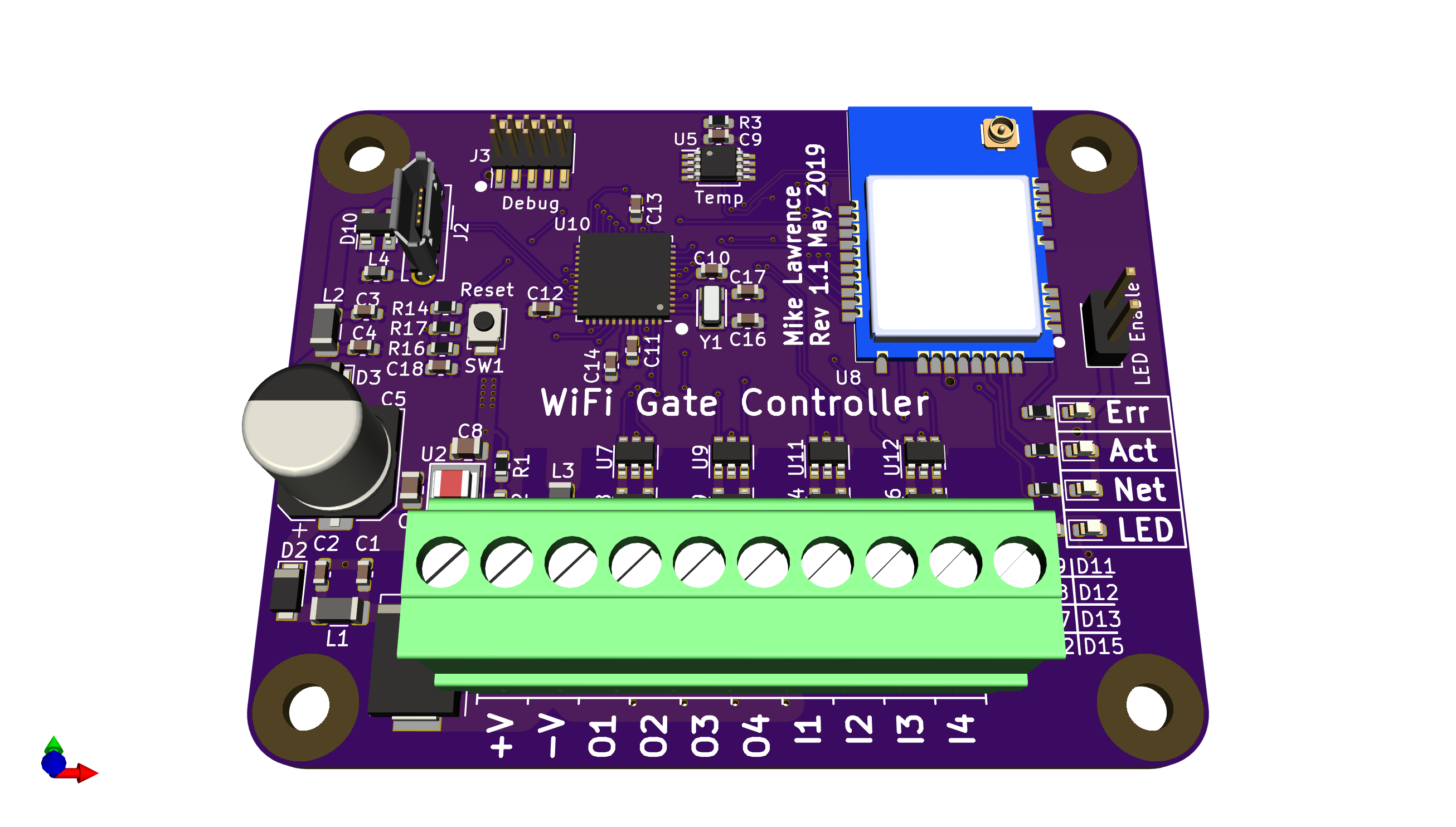
After years of using weak garage door openers and trying to position them just right so my solar powered gate 400′ away would open when needed I decided it was time to make a wireless controller of my own. 802.11 is a ubiquitous choice and with the right antenna range is not a problem. Two wireless modules consistently popped up when searching for low power embedded WiFi, ESP8266 and ATWINC1500. In the end I chose the ATWINC1500 module for it’s compatibility with Arduino and it’s low power modes. This board is fully compatible with the Arduino MRK1000 which includes a SAMD21G18 Arm processor and the ATWINC1500 module. I also chose to use MQTT. Recent projects showed how effective the MQTT client/server model is in this situation. I use Home Assistant for home automation and it directly supports MQTT.
This board is designed for and tested with a US Automation Gate Opener.
Note: The LMZ21700 Simple Switcher, SAMD21G18 ARM Processor, and ATWINC1500 WiFi Module have exposed pads on the bottom which requires either a reflow oven or hot air to solder properly.
For Bill of Materials generation, I use my version of KiBoM forked from SchrodingersGat.
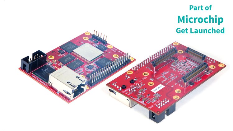
PolarBerry is a System on Module (SoM) SBC utilizing the Microsemi PolarFire SoC, which integrates a low-power FPGA with a highly-secure, four-application-core, 64-bit RISC-V subsystem that is Linux-capable.
Application Flexibility
PolarBerry is designed to be application-flexible, while also being quick to use and deploy. Its combination of features make it perfect for applications that require high-performance but a low power draw, defense-level security, a real-time, deterministic RISC-V processor that’s capable of Linux, a small physical profile, immediate connectivity, or custom extensibility – such as those in the autonomous vehicle or defense industries.
FPGA, RISC-V, and Linux
PolarBerry with its PolarFire SoC provides a system with hardcore, deterministic, coherent RISC-V processing and programmable logic – enabling real-time systems and Linux with unparalleled security features.
SBC and SoM Form-factor
As the board is essentially an SBC in a SoM form-factor, it can be utilized as a standalone module or along with a carrier board like the Sundance DSP SE215 carrier or one of your own designs.
A Raspberry Pi connector, two CAN bus interfaces, and an RJ45 port for Ethernet allows PolarBerry to tap into extensive ecosystems, and its Samtec connectors provide high-speed communication to a carrier board for powerful peripheral customization.
For example, PolarBerry works well with our SE215 PCIe SoM carrier board which provides access to an FMC and additional interfaces like an SFP+ module.
SiTime Corporation announced that it has entered the $2 billion precision resonator market with the ApexMEMS family of MHz resonators. These new devices are the third-generation of SiTime silicon ctechnology and are available in a variety of MHz frequencies for high-volume electronics. Mobile and IoT applications such as Bluetooth wearables and wearables, high-speed connectivity interfaces, asset-tracking, as well as microcontrollers, can take advantage of the 85% space savings, integration, consistent performance, resilience, and reliability that are offered by ApexMEMS resonators.
According to estimates by Dedalus Consulting and SiTime, the resonator market is $3 billion in size and consists of three product categories – approximately $2 billion of precision resonators, $400 million of ceramic resonators, and $600M of SAW resonators. By 2024, industry analysts and SiTime estimate that 25 to 30 billion precision resonators will be sold, driven by the growth of connectivity in mobile-IoT, industrial-IoT, automotive, and industrial electronics. It is expected that up to 30% of these resonators will need to be very small, offer higher performance, and be easily integrated into system-in-packages and modules. This high-value market is one use case for ApexMEMS resonators.
For integration into standard IC packages and modules, ApexMEMS resonators are available as a silicon die. Co-packaging these resonators with high-performance semiconductors such as Bluetooth chips and microcontrollers gives customers a significant system and development advantage.
When using a quartz resonator, engineers face numerous challenges. Significant effort goes into matching the oscillator circuit with the resonator in the presence of unknown board parasitics. Without proper matching, performance may be suboptimal, and device startup at cold temperatures may be impacted. This situation gets even more complicated due to performance variations that are inherent in quartz resonators. An integrated ApexMEMS solution solves these challenges, reduces development time, simplifies manufacturing, and boosts system performance, reliability, and resilience.
ApexMEMS resonators offer similar advantages in standalone applications. Integrated load capacitors help reduce the system size through the elimination of discrete passive components. Board layout and routing is simplified considerably, especially in space-constrained mobile-IoT applications. With the closer placement of the resonator to the semiconductor device, system performance is greatly improved.
ApexMEMS-based timing solutions deliver up to seven times better phase noise performance at half the power than our previous generation. At a tiny 0.42 mm x 0.42 mm size, the ApexMEMS resonators are 85% smaller than a typical quartz resonator, and also integrate the load capacitors. These new resonators provide stability as good as ±20 ppm while delivering superior reliability and best-in-class environmental resilience, like other SiTime devices. ApexMEMS resonators operate reliably at temperatures as high as 125oC, a useful feature when integrated inside plastic packages.
Automotive Grade Devices Offer High Ripple Currents Up to 3.8 A, Operating Temperatures to +105°C, and Useful Life of 10,000 Hours at 105°C
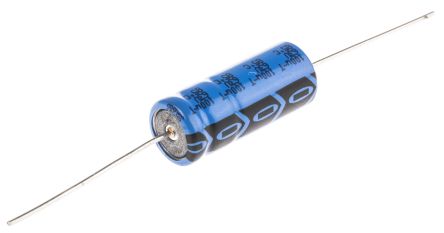
Vishay Intertechnology, Inc. today introduced a new series of low impedance, Automotive Grade miniature aluminum electrolytic capacitors that combines high ripple currents up to 3.8 A with high temperature operation to +105 °C and very long useful life up to 10,000 h at 105°C.
Compared to previous-generation solutions, Vishay BCcomponents 170 RVZ series capacitors offer lower impedance and 10 % to 15 % higher ripple current. This allows designers to utilize fewer components, increasing design flexibility and saving board space. In addition, the AEC-Q200 qualified devices are available in smaller case sizes, ranging from 10 mm by 12 mm up to 18 mm to 40 mm.
Features
Very long useful life: 4000 h to 10000 h at 105 °C, high stability, high reliability
Very low impedance and low ESR in smaller case sizes than the 150 RMI series
Excellent ripple current capability
Applications
Power supplies (SMPS, DC/DC converters) for general industrial, EDP, audio‑video, automotive, and telecommunications
Smoothing, filtering, buffering
Featuring radial leads and a cylindrical aluminum case, insulated with a blue sleeve, the 170 RVZ series offers rated voltages up to 63 V, capacitance from 100 µF to 6800 µF, and low impedance. The capacitors are charge- and discharge-proof.
As polarized aluminum electrolytic capacitors with a non-solid electrolyte, the RoHS-compliant devices are ideally suited for smoothing, filtering, and buffering in switch mode power supplies and DC/DC converters for industrial, automotive, telecommunications, medical, and consumer applications.
Samples and production quantities of the 170 RVZ series are available now, with lead times of six weeks. More information please visit https://www.vishay.com/ppg?28462.
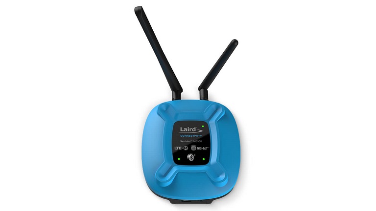
Laird has introduced Sentrius™ MG100 micro-gateway with LTE-M/NB-IoT and Bluetooth 5
Based on Laird Connectivity’s Pinnacle 100 modem, the Sentrius MG100 Gateway captures data from Bluetooth 5 sensors and sends it to the cloud via a global low power cellular (LTE-M/NB-IoT) connection. Supports LTE bands 1, 2, 3, 4, 8, 12, 13, 20, and 28.Based on the Sierra Wireless HL7800 module, the MG100 includes Bluetooth 5 features like CODED PHY, 2M PHY, and LE Advertising extensions.
Key features
Wireless connectivity
Flexible power options
Certified for global deployment
Antenna choices
Additional features
LTE-M / NB-IoT radio via Sierra Wireless HL7800 module (Chipset: Altair ALT1250)
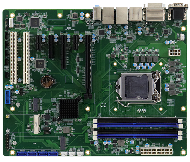
IBASE Technology Inc., a leading manufacturer of industrial motherboard and embedded systems, has rolled out the MB997 ATX motherboard for 9th Gen Intel® Core™ i7/i5/i3 and Xeon® processors. The Intel® C246/Q370/H310-based motherboard is designed for diverse applications, such as industrial automation, AI integrated systems, and smart retail systems.
The latest MB997 delivers high-performance computing for demanding industrial applications while providing multiple connectivity, expansion and functionality to meet customer requirements. The board supports up to 7 expansion slots including 1x PCI-E(x16), 1x PCI-E(x8)/Gen3.0, 1x PCI-E(x4), 2x PCI-E(x1), and 2x PCI, as well as 6x USB3.1, 2x USB 2.0, 2x SATA 3.0, and 6x COM ports. It can handle up to 128GB DDR4 memory across four slots and support three independent outputs (HDMI 2.0a, DVI-D, and DisplayPort) with 4K resolution each.
The board is loaded with advanced features such as TPM (2.0) hardware-based security to ensure platform integrity, iSMART 4.0 technology that enables power saving, power on/off and power resumption, and also NVMe and CNVi interfaces that bring various performance improvements. Like all IBASE industrial motherboards, MB997 comes with strict revision control, modification control and long-term support. Operating systems supported are Win10 IoT Enterprise and Linux Ubuntu.
MB997 FEATURES:
9th Gen Intel® Xeon® E / Core™ i7/i5/i3 processors
4x DDR4 DIMM, Max.128GB
Intel® processor integrated graphics supports HDMI(2.0a), DVI-D, and DisplayPort
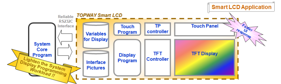
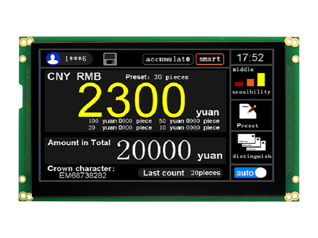
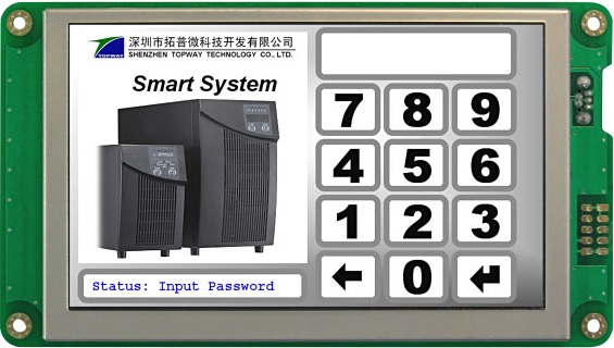
Shenzhen Topway Technology Co.Ltd. has launched their TOPWAY Smart TFT LCD module, which embeds LCD driver, controller and MCU, in a color LCD module with digital brain. A thin-film-transistor liquid-crystal display (TFT LCD) is a variant of a liquid-crystal display (LCD) that uses thin-film-transistor (TFT) technology to improve image quality such as brightness and contrast.
A TFT LCD is an active matrix LCD, in contrast to passive matrix LCDs or simple, direct-driven LCDs with a few segments. Smart TFT LCD sets engineer free from tedious display programming, so that product engineer can focus on product development. Smart TFT LCD module can help users greatly reduce product’s time-to-market. And the product is more reliable with high EMI tolerance.
Taking over the duty of displaying content and respond to touch event, Topway launched Smart LCD module couple years ago. Smart LCD is a TFT LCD display module embedded with MCU, display engine and touch controller. Simple serial commands are all that is needed to interact with the screen, no more pixel programming.
Smart LCD module is between traditional TFT LCD module and HMI device. HMI device works as a standalone unit with higher cost. Topway Smart TFT LCD provides a cost effective way to quickly implement human – machine interface:
Graphical UI Editor, enables quick user interface construction, speeds up product’s time-to-market
Preloaded UI design in smart LCD, provides speedy showing and updating
Embedded display engine, reduces main board workload and over-all cost
Built-in Lue Script language engine, empowers rich and friendly user interface
RJ45 port, supports long-distant update and easy expansion
Unified body, improves EMC performance and increases reliability
Smart LCD module works with five basic items:
Page – container for one UI screen, it holds page elements
Element – functional display unit on a page. Such as Action, Character, Image etc.
-9 action type elements
-6 character type elements
-6 image type elements
-8 graphic type elements
Call Function – function that can be triggered by Page start, Touch Key or Virtual Touch Key press action
-14 keyboard functions
-20 operations
VP Variable – a RAM area for holding temporary value. It supports host access, on-screen keyboard input and value operations
Image Resource – images linked by elements or pages for displaying, including background images, icon and animated images
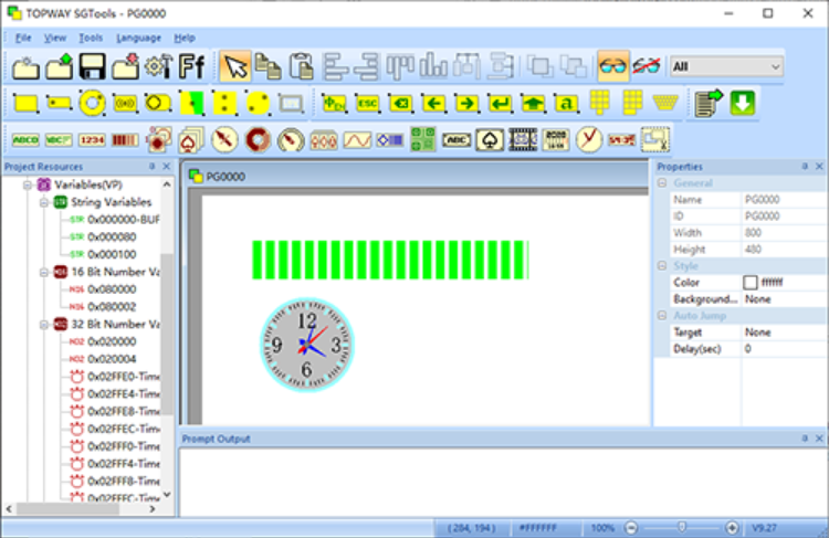
Topway’s UI Editor for smart LCD module provides a zero-coding way to construct human machine interface. User can drag & drop above basic items onto page and set up their properties according to need. You can find a short video demonstrating on how to build user interface in minutes with Smart LCD Module:
You can find more information about Smart LCD module by visiting the product page.
In most of our previous tutorials concerning operational amplifiers, only one input was applied to either the inverting or non-inverting op-amp’s input. This new article will deal with a configuration known as the summing amplifier which gives an output that is proportional to a weighted sum of the multiple inputs present.
The inputs can either be applied to the inverting or non-inverting branches which give two possible configurations that will be separately presented in the first and second sections. They are commonly referred as the inverting summing amplifier and non-inverting summing amplifier and we will see what are their differences and similarities.
In a third section, the dual configuration of the summing amplifier, the subtracting amplifier, is investigated.
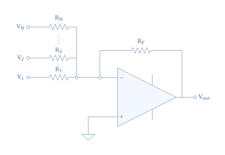
Inverting summing amplifier
In Figure 1 we see the general circuit for an inverting summing amplifier:
In this configuration, N inputs V1,V2,…,VN are applied to the inverting input of the op-amp through different resistor R1,R2,…,RN. The output Vout is feedbacked to the inverting branch through a resistor RF, the non-inverting input is grounded.
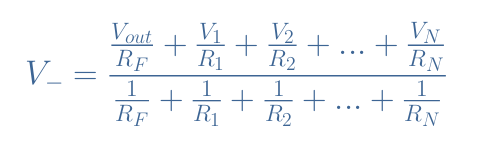
We can apply Millman’s theorem to V– in order to demonstrate the output relation of this circuit:
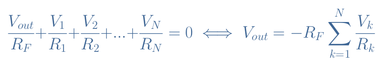
With the hypothesis of the ideal op-amp, i+=i–=0, and V+=V–=0, which leads to the output relation of the inverting summing amplifier:
eq 1: Output formula of the inverting summing amplifier
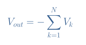
It is interesting to note that if we equalize all the input resistors with the feedback resistor, R1=R2=…=RN=RF, we obtain a simplified version for Equation 1:
eq 2: Simplified output formula with the resistor equality condition
In this case, the sum is not weighted anymore, and the inverting summing amplifier adds the inputs negatively as the output signal phase is in opposition with the inputs.
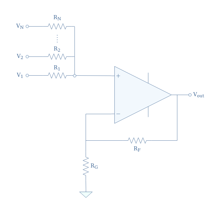
Non-inverting summing amplifier
The non-inverting summing amplifier is a similar configuration to the inverting summing amplifier. However, the inputs here are applied to the non-inverting input while the inverting branch is connected to both the op-amp’s output through a feedback resistor RF and grounded through a resistor RG.
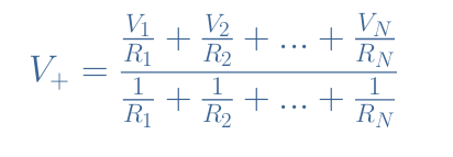
We can apply Millman’s theorem to V+ in order to demonstrate the output relation of this circuit:
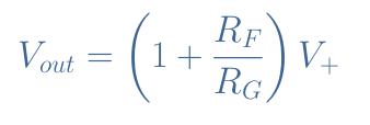
Since the voltage gain Vout/Vin=Vout/V+ of a non-inverting configuration is given by 1+(RF/RG), we can conclude that the general relation for the non-inverting summing amplifier output is given by Equation 3:
eq 3: Output formula of the non-inverting summing amplifier
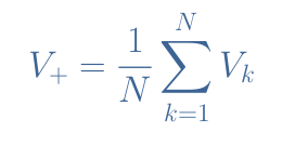
The expression of V+ can be extremely simplified if we pose R=R1=R2=…=RN, we get indeed:
Moreover, we can also pose (1+RF/RG)=N in order to get a direct sum of the input voltages:
eq 4: Simplified output formula with the resistor equality condition
With these two conditions, we can see that the output voltage is a direct sum of the input signals as the sum is not weighted and no phase difference is present.
To conclude this section we can draw a little comparison between the inverting and non-inverting summing configurations. The advantage of the inverting configuration is that even in the general case, the output is simply expressed as a function of the different resistor and input values.
In a non-inverting configuration, the output is always in phase with the inputs which save the trouble to use an inverting buffer to rectify the signal. Moreover, the non-inverting configuration presents the property of having a much higher input impedance which is an advantage to properly inject the desired voltages from a source (microphone for example) to the inputs of the op-amp.
However, we have seen that the output voltage is a simple weighted sum only under a condition of equality between all the resistors in the circuit.
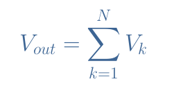
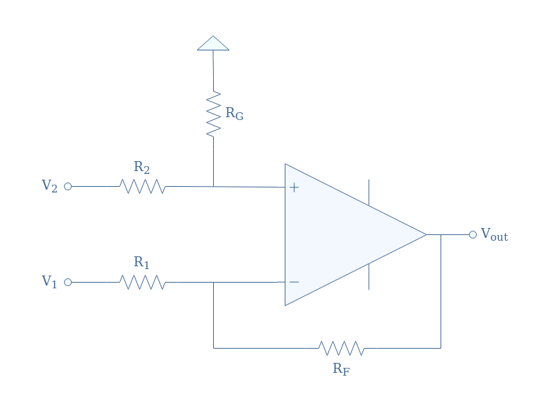
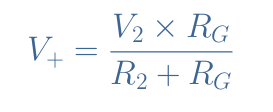
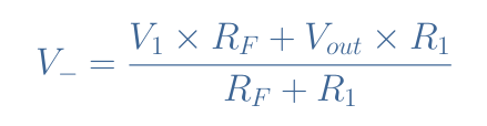
Subtracting amplifier
If the inputs are both applied to the inverting and non-inverting pins of an op-amp, a subtracting configuration is realized such as presented in Figure 3:
The voltage V+ can be expressed by a voltage divider formula:
The voltage V– is expressed thanks to Millman’s theorem:
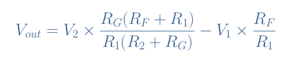
After reminding that V+=V–, a few steps of simplification lead to the general output expression of the subtracting amplifier:
eq 5: Output formula of the subtracting amplifier
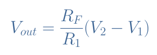
We can simply show by equalizing the two factors that if the condition RFR2=RGR1 is met, the output formula can be simplified to Equation 6:
eq 6: Simplified output formula for the subtracting amplifier
This condition can be achieved by equalizing all the resistances: R1=R2=RG=RF. In that case, since RF=R1, Equation 6 can be reduced to a direct subtraction Vout=V2-V1.
Applications
Audio mixer
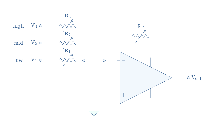
Consider an inverting summing amplifier with three inputs such as presented in Figure 4:
fig 4: Simple audio inverting summing amplifier
The resistors here are replaced by potentiometers in order for a user to directly control the output signal.
This type of configuration can be used in the audio domain where different pitches can be separately processed through an amplifier before being added together with possibly different prefactors.
Typically, the frequency ranges are given by:
low: 20 Hz to 500 Hz
mid: 500 Hz to 6 kHz
high: 6 kHz to 20 kHz
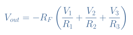
According to Equation 1, the output signal of this configuration is given by:
We can clearly identify that the potentiometer RF controls the global gain of the output, increasing or decreasing its value will simultaneously affect all the frequencies. On another hand, the potentiometers R1, R2, R3 only affect respectively the low, mid, and high pitches and they will enable the user to balance or unbalance certain frequencies.
We can note that if we want the output to be in phase with the different inputs, a simple inverting buffer can be used to rectify it.
Digital to Analogue Converter (DAC)
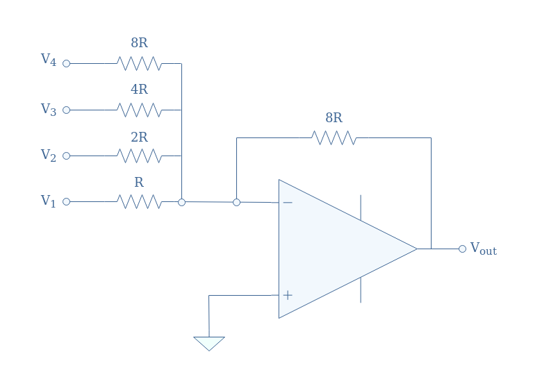
A DAC is a summing amplifier based circuit that converts binary data (0 and 1) into an analog signal (a real number). An example of this circuit with four binary inputs known as a four-bit DAC and is presented in Figure 5:
fig 5: Four-bit DAC circuit representation
The values of the resistor are not chosen randomly, their values always need to double from the previous branch. This ensures a proper conversion from a binary number to a decimal number.
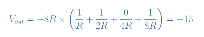
As an example, consider the binary four-bit input 1101 (V1=1 ; V2=1 ; V3=0 ; V4=1). According to Equation 1, the output is given by:
This validity of this result can be confirmed when we manually convert the same input to a decimal number: (1101)decimal=(1×23)+(1×22)+(0×21)+(1×20)=13.
In practice, the circuit shown in Figure 5 can only be implemented up to a certain number of bits depending on the precision of the resistors that must exactly double their value for each added bit. An alternative circuit known as the R-2R Ladder DAC is preferred for higher binary numbers.
Conclusion
A summing amplifier can either be based on an inverting or non-inverting configuration. Despite the high input impedance and in-phase output signal that the non-inverting summing amplifier can provide, the inverting summing amplifier is more common as it’s output is a simple weighted sum.
Indeed, the non-inverting summing output is a simple weighted or direct sum of the inputs only when a condition of equality between all the resistors in the circuit is met.
After presenting and detailing these two summing configurations, a third section has presented the subtracting amplifier which slightly differs from the summing amplifiers and is used to subtract two or more signals by applying them both on the inverting and non-inverting pins.
Finally, in the last section, we present the possible applications of the summing amplifiers. Indeed, an inverting summing amplifier can be used as an audio mixer in order to separately control each input importance, the inputs can, for example, be frequency ranges or different instruments outputs.
We also show that summing amplifiers can be used as a simple digital to analog converters when the resistance value for each added bit is doubled.