Smart LED Dimmer Controlled via Bluetooth

Author: Anas Ajaj for Dialog Semiconductor

Introduction

This article describes how to build a smart digital dimmer. A dimmer is a common light switch that is used in houses, hotels and many other buildings. Older versions of dimmer switches were manual, and would typically incorporate a rotary switch (potentiometer) or buttons to control the light level. This article describes how to build a digital dimmer that has two ways of controlling light intensity; a smartphone and physical buttons. The two modes can work seamlessly together so that the user can increase or decrease luminosity from both a button and smart phone. The project is implemented using a SLG46620V CMIC, HC-06 Bluetooth module, push buttons and LEDs.

We are going to use the SLG46620V CMIC as it helps minimize discrete project components. GreenPAK IC’s are small and have multiuse components, which allows a designer to decrease components and to add new features. Additionally, the project cost is subsequently reduced.

The SLG46620V also contains a SPI connection interface, PWM blocks, FSM and a lot of useful additional blocks in one tiny chip. These components allow a user to build a practical smart dimmer which can be controlled via a Bluetooth device or wall buttons, support extended-time dimming, and the addition of selectable features without using a microcontroller or expensive components.

Project features:

Two methods of control; mobile app and real buttons.

Smooth on-off transition for the light. This is healthier for a consumer’s eyes. It also gives a more luxurious feeling, which is appealing to hotels and other service industries.

Sleep mode feature. This will be an added value for this application. When the user activates this mode, light brightness decreases gradually in 10 minutes. This helps people who suffer from insomnia. It is also useful for kid’s bedrooms and retail shops (closing time).

Project Interface

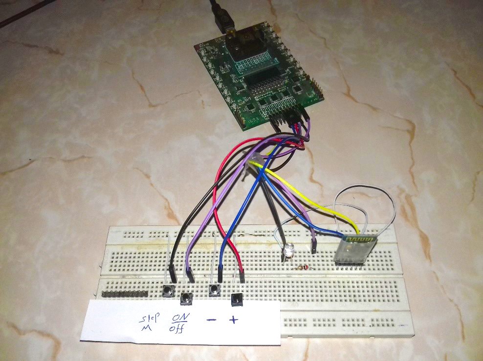
The project interface has four push buttons, which are used as GreenPAK inputs:

  • ON\OFF: turn the light ON\OFF (soft-start\stop).
  • UP: increase light level.
  • Down: decrease light level.
  • Sleep Mode: by activating sleep mode, light brightness decreases gradually over a period of 10 minutes. This gives the user time before sleeping and guarantees that the light will not stay ON all night.

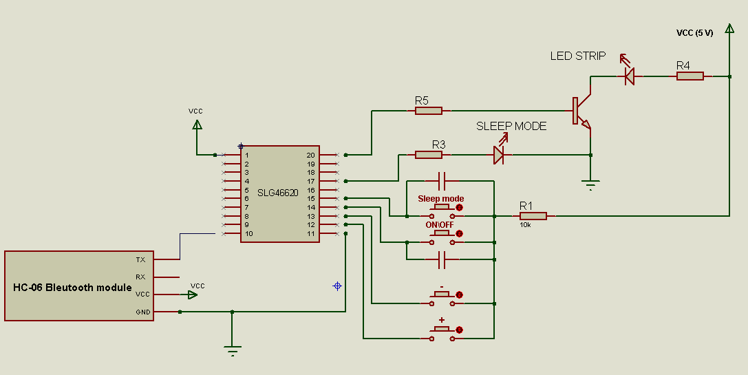
The system will output a PWM signal, which will be passed to an external LED and sleep mode LED indicator.

Figure 1: Dimmer Block Diagram

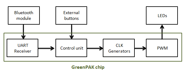
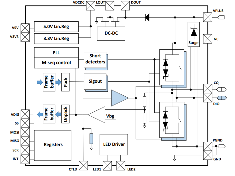
The GreenPAK design is comprised of 4 main blocks. The first is a UART receiver, which receives data from the Bluetooth module, extracts orders, and sends them to a control unit. The second block is a control unit, which receives orders coming from the UART receiver or from the external buttons. The control unit decides the required action (Turn ON/OFF, Increase, decrease, enable sleep mode). This unit is implemented using LUTs.

The third block supplies the CLK generators. In this project, a FSM counter is used to control the PWM. The FSM’s value will change (up, down) according to the orders given by 3 frequencies (high, medium, and low). In this section the three frequencies will be generated and the required CLK passes to FSM according to the required order; In turning on/off operation, high frequency passes to FSM to soft start/stop. During dimming, the medium frequency passes. The low frequency passes in sleep mode to reduce the FSM value more slowly. Then, light brightness decreases slowly too. The fourth block is the PWM unit, which generates pulses to external LEDs.

GreenPAK Design

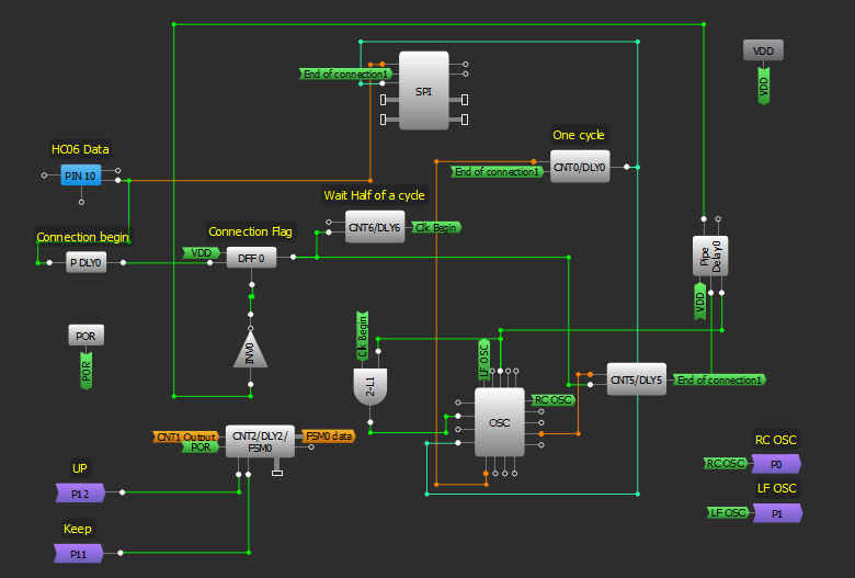
The best way to build a dimmer using GreenPAK is by using the 8-bit FSM and a PWM. In the SLG46620, FSM1 contains 8 bits and can be used with PWM1 and PWM2. The Bluetooth module must be connected, which means the SPI parallel output must be used. The SPI parallel output bits 0 through 7 connections are muxed with DCMP1, DMCP2, and LF OSC CLK, OUT1, OUT0 OSC outputs. PWM0 obtains its output from FSM0 (16 bits). FSM0 does not stop at 255; it increases up to 16383. To limit the counter value at 8 bits another FSM is added; FSM1 is used as a pointer to know when the counter reaches 0 or 255. FSM0 was used to generate the PWM pulse. As the two FSM’s values must be changed at the same time to have the same value, the design becomes a bit complex where in both FSMs have a predefined, limited, selectable CLK. CNT1 and CNT3 are used as mediators to pass the CLK to both FSMs.

The design built in GreenPAK Designer Software (.gp file can be found here) consists of the following sections.

UART Receiver

First, we need to set up the HC06 Bluetooth module. The HC06 uses the UART protocol for communication. UART stands for Universal Asynchronous Receiver / Transmitter. UART can convert data back and forth between parallel and serial formats. It includes a serial to parallel receiver and a parallel to serial converter which are both clocked separately. The data received in the HC06 will be transmitted to our GreenPAK device. The idle state for Pin 10 is HIGH. Every character sent begins with a logic LOW start bit, followed by a configurable number of data bits, and one or more logic HIGH stop bits.

The HC06 sends 1 START bit, 8 data bits, and one STOP bit. Its default baud rate is 9600. We will send the data byte from the HC06 to the GreenPAK SLG46620V’s SPI block.

Since the Dialog SPI block does not have START or STOP bit control, those bits are instead used to enable and disable the SPI clock signal (SCLK). When Pin 10 goes LOW, the IC has received a START bit, so we use the PDLY falling edge detector to identify the start of communication. That falling edge detector clocks DFF0, which enables the SCLK signal to clock the SPI block.

Our baud rate is 9600 bits per second, so our SCLK period needs to be 1/9600 = 104 µs. Therefore, we set the OSC frequency to 2 MHz and used CNT0 as a frequency divider.

2 MHz-1 = 0.5 µs

(104 µs / 0.5 µs) - 1 = 207

Therefore, we want the CNT0 counter value to be 207. To ensure that data is not missed, a half clock cycle delay on the SPI clock is added so that the SPI block is being clocked at the proper time. This is accomplished by using CNT6, 2-bit LUT1, and the OSC block’s External Clock. The output of CNT6 does not go high until 52 µs after DFF0 is clocked, which is exactly half of our SCLK period of 104 µs. When it goes high, the 2-bit LUT1 AND gate allows the 2 MHz OSC signal to pass into the EXT. CLK0 input, whose output is connected to CNT0.

Figure 2: UART Receiver

Control Unit

In this section, commands will be executed according to the received byte from the UART receiver, or according to the signals from the external buttons. Pins 12, 13, 14, 15 are initialized as inputs and are connected to external buttons.

Each pin is internally connected to an OR gate input, while the second input of the gate is connected with the corresponding signal that coming from the smartphone via Bluetooth which is going to appear on SPI Parallel output.

DFF6 is used to activate sleep mode where its output changes to high with the rising edge coming from 2-bit LUT4, while DFF10 is used to maintain the lighting status, and its output changes from low to high and vice versa with every rising edge coming from 3-bit LUT10 output.

FSM1 is an 8-bit counter; it gives a high pulse on its output when its value reaches to 0 or 255. Consequently, it’s used to prevent FSM0 (16-bit) from exceeding the value 255, as its output resets DFFs and it changes DFF10 status from on to off and vice versa if the lighting is controlled by the buttons +, and the maximum/minimum level has been reached.

The signals connected to FSM1 inputs keep, up will reach FSM0 through P11 and P12 to synchronize and keep the same value on both counters.

Figure 3: Control Unit Design

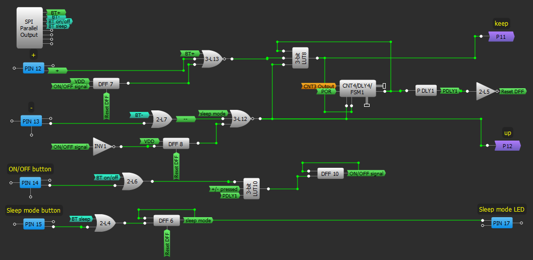
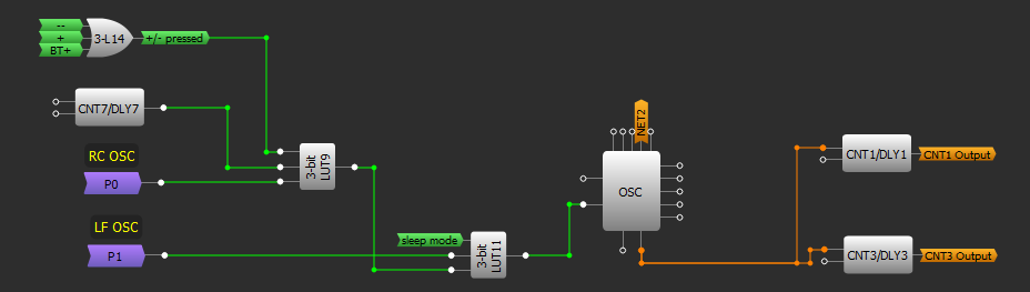
CLK Generators and Multiplexer

In this section, three frequencies will be generated, but only one will clock the FSMs at any one time. The first frequency is RC OSC, which is fetched from the matrix 0 through P0. The second frequency is LF OSC which is also fetched from the matrix 0 through P1; the third frequency is the CNT7 output.

3-bit LUT9 and 3-bit LUT11 allow one frequency to pass, according to the 3-bit LUT14 output. After that, the chosen clock transmits to FSM0 and FSM1 through CNT1 and CNT3.
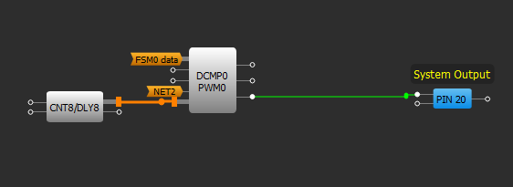
Figure 4: Clock Generator Design

PWM

Finally, FSM0 value transforms to PWM signal to appear through pin 20 which is initialized as an output and it is connected to the external LEDs.

Figure 5: PWM Block

Android app

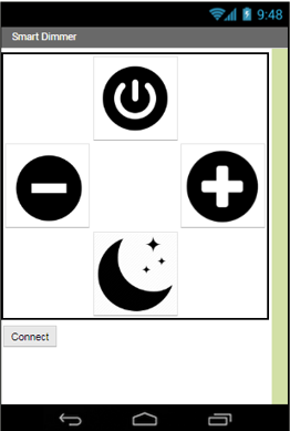
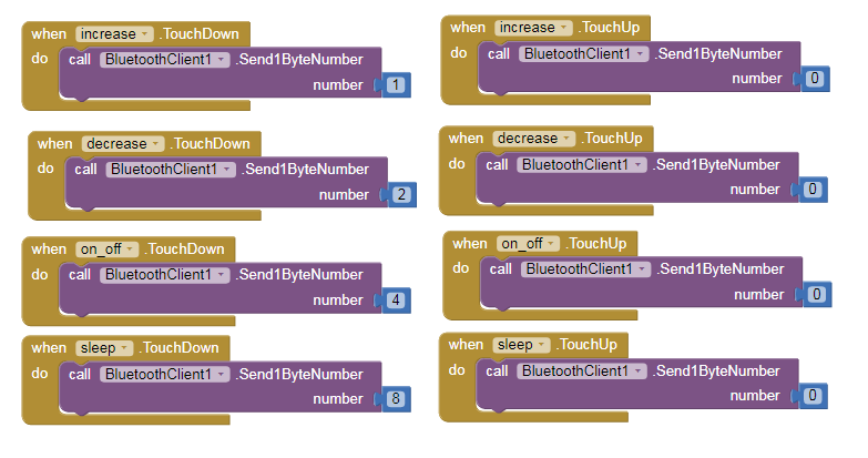
The Android app has a virtual control interface similar to the real interface. It has five buttons; ON\OFF, UP, DOWN, Sleep mode, and Connect. This Android Application will be able to convert button presses into a command and will send the commands to the Bluetooth module to be carried out.

This app was made with MIT App Inventor, which doesn’t require any programming experience. The App Inventor lets the developer create an application for Android OS devices using a web browser by connecting programming blocks. You can import our App into the MIT App Inventor by clicking on Projects -> Import project (.aia) from my computer, and selecting the .aia file included with this folder.

To create the Android Application a new project must be started. Five buttons are required: one is a list picker for Bluetooth devices, and the others are the control buttons. We need to add a Bluetooth client as well. Figure 6 is a screen capture of our Android Application’s user interface.

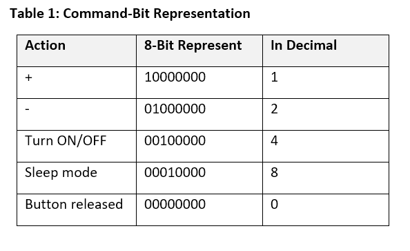
After we add the buttons, we are going to assign software function for each button. We are going to use 4 bits to represent the status of the buttons. One bit for each button, therefore, when you press the button, a specific number will be sent via Bluetooth to the physical circuit.

Figure 6: Programming Blocks of Buttons

These numbers are shown in Table 1:

Table 1: Command-Bit Representation
Figure 7: Programming Blocks of Buttons
Figure 8: Circuit Schematic
Figure 9: Prototype Interface

Conclusion

This article describes a smart dimmer that can be controlled in two ways; an Android app and real buttons. Four separate blocks are outlined within the GreenPAK SLG46620V which control the process flow for increasing or decreasing the PWM of a light. Additionally, a Sleep-mode feature is outlined as an example of extra modulation available for the application. The example shown is low voltage, but can be modified for higher voltage implementations.

Flash Graphene Synthesis – Electricity Turns Garbage into Graphene

Graphene is the thinnest yet one of the most strong materials known to man while being only one atom thick. On top of that, graphene is an excellent conductor of heat and electricity and has remarkable light absorption abilities. It is truly a material that could change the world, with unlimited potential for integration in almost any industry. But the current processes of making it the right form is very time consuming and expensive.

Here comes a light of hope from the researchers at Rice University. They have reported in Nature that they can zap almost any source of solid Carbon into graphene. Be it any food scraps or old car tires, anything can be turned into perfect graphene sheets for various applications ranging from high-strength concrete to flexible electronics. Examples of Graphene’s usage can be found in the hall effect sensor, flexible terahertz sensor, and in many other fields.

“This work is pioneering from a scientific and practical standpoint”

as it has the potential to make graphene cheap enough to use to strengthen asphalt or paint, says Ray Baughman, a chemist at the University of Texas, Dallas. The researchers have founded a startup company called “Universal Matter” to commercialize their “waste-to-graphene” process.

Since the discovery of Graphene in 2004, high-quality graphene of either single sheets or just a few stacked layers has remained very expensive to produce and purify on an industrial scale. The making of graphene by depositing from a vapor or exfoliation method, are too costly for many high-volume applications. And higher throughput approaches, such as the famous peeling graphene from chunks of graphite, produce sheets of graphene composed of up to 50 graphene layers that are not ideal for most applications.
In 2014, James Tour, a chemist at Rice University, and his colleagues found they could make a pure form of graphene by heating carbon black for a fraction of a second up to 3000 Kelvin with a powerful laser. As the cloud of carbon cooled it was made into the most stable structure of graphene. But the approach still produced only tiny qualities and required a lot of energy and precision.

James Tour and Duy Luong show a sample of pure turbostratic flash-graphene

Almost two years ago, Luong Xuan Duy, one of Tour’s grad students, had created metal nanoparticles by zapping a material with electricity. So, he put a small chunk of carbon black in a clear glass vial and applied 400 volts for about 200 milliseconds almost reaching the temperature inside the vial about 3000 Kelvin. Later on, chemical tests revealed he had produced graphene.

It turned out to be a type of graphene that is ideal for bulk uses. As the carbon atoms condense to form graphene, they don’t have time to stick in a regular pattern, as they do in graphite.

This will make it a very good material for applications,

  • says Monica Craciun, a materials physicist at the University of Exeter.

When they added just 0.05% by volume of their flash-produced graphene to concrete, the compressive strength rose almost 25%. Fortunately, the starting point for flash graphene could hardly be cheaper or more abundant for this kind of bulk use. As we have seen, virtually any organic matter can be zapped with electricity to make graphene.

As Duy puts it,

We’re turning garbage into graphene.

So, in near future, this new process can ignite the long-anticipated graphene revolution in electronics and elsewhere.

L6364Q Dual-Channel Transceiver IC for SIO and IO-Link sensor applications

ST Microelectronics is bringing a bridge between a microcontroller capable of sensing/actuation and a 24 V power supply in industrial sensor applications with the L6364Q, a dual-channel transceiver IC, which brings dual communication channels, allowing for a configurable output with extra driving power, along with support for IO-Link, a DC / DC converter and a dual-mode UART.

The L6364Q transceiver IC brings some interesting hardware to the table: from linear and DC-DC regulators to configurable limiting current thresholds and many, many protection measures. As stated, the transceiver supports IO-Link (at COM2, with 38.4 kbaud and COM3, with 230.4 kbaud), as well as standard Single-Input / Output communication. In normal operation, the L6364Q is configured by the microcontroller at startup, through SPI. Then, it operates as a Single Input Output IO-Link device, controlling the input lines configured by the microcontroller. The device can also act as a physical layer between the microcontroller and an IO-Link master, which, when connected to it, the master can communicate with the microcontroller.

Regarding features, the L6364Q transceiver has:

  • Supply voltage range from 5 to 35 V
  • Linear regulators (5 and 3.3 V, at 50 mA current)
  • DC-DC regulator with configurable frequency (ranging from 0.5 MHz to 2 MHz) and voltage (from 5 to 10.5 V), with 50 mA current
  • Low dissipative (5 ohm) output stages for CQ and DIO, configurable in high side, low side or push / pull. Switching time of 100 ns (load of 2 kohm // 2.2 nF)
  • Configurable current limitation threshold for the CQ and DIO lines (from 110 mA to 250 mA) and in join mode (from 220 mA to 500 mA)
  • Full set of protection measures:
    • Embedded reverse polarity diode on the DOUT pin
    • Full zero current reverse polarity between the Vplus, CQ, DIO and PGND pins
    • Configurable thermal shutdown threshold, up to 216 ºC
    • 7-bit temperature measurement, calibrated
    • Configurable undervoltage protection on the Vplus pin (from 6.0 to 15 V)
  • Operating voltage ranging from -40 to 150 ºC
  • Capable of driving inductive, resistive and capacitive loads
  • Quartz-free IO-link clock extraction and timing generation for the COM2 (38.4 kBaud) and COM3 (230.4 kBaud)
  • Integrated UART with M-sequence handling (checksum included) for the IO-Link sequences according to version 1.1 of the specification
  • Single octed UART mode for unlimited M-sequence size and continuous data transfer
  • Internal data buffer of up to 15 octets
  • Transparent UART mode for special applications
  • 8 V zener for fast demagnetization of inductive loads
  • Two configurable LED drivers (up to 8 mA current)
  • QFN-20L 4×4 mm package
Block diagram of the L6364Q transceiver IC

Besides the aforementioned set of features, the transceiver guarantees ESD (for up to 4 kV) and EMC (2 A / 50 us, with 500 ohm coupling) protection. It has possible uses in industrial sensors and actuators, factory automation, process control, and as a switch driver of resistive, inductive, and capacitive loads, among other things. Lastly, it comes at a price of around $4.83. 

L6364Q ST-Link: https://www.st.com/en/power-management/l6364.html

Vecow Launched MTC-8000 Series Energy-Efficient Multi-Touch Computer

Vecow Co., Ltd., a team of global embedded experts, announced the release of the latest Industrial Multi-Touch Computer, MTC-8000 Series. Powered by energy-efficient Intel Atom™ x7-E3950 processor with Intel® HD Graphics 505 chipset, MTC-8000 Series provides astounding 3D rendering, media composting and video encoding and brings more powerful system performance than ever.

Vecow MTC-8000 Series offers a variety of display sizes from 10.1” to 21.5″ LED backlight control type industrial-grade LCD. It also features projected capacitive touch technology with 10-point multi-touch function for highly responsive sensing and has up to 7H hardness anti-scratch touch surface. Designed with a truly flat surface, Vecow MTC-8000 Series prevents water and dust accumulation on the system and allows for easy cleaning after each use.

Vecow MTC-8000 provides various I/O ports including 4 USB ports, 2 Intel GigE LAN, 2 COM with RS-232/422/485, an easy-access 2.5” SATA SSD/HDD and a full-size mSATA for data storage that fulfills customers’ needs in each application. Users could also use internal mini PCIe to install 3rd party wireless modules, such as 4G/3G/LTE/GPS/WiFi/Blue tooth devices or expansion I/O modules to satisify customers’ requirements in various environments. The MTC-8000 Series also provides panel mount, VESA mount and Stand kit for easy deployment in diverse industrial environments. Vecow MTC-8000 Series is the best selection to build systems, self-service control panels, outdoor Kiosks and many other industrial applications.

“Vecow MTC-8000 Series comes with a widescreen design that provides more operation area than standard 4:3 LCD with more space to process data, “

said Alan Chou, Senior Product Manager, Embedded Systems & Platform Division at Vecow.

“It also provides external SSD/HDD kit for easy system maintenance. With flexible expansion I/O ports to expand or integrate with 3rd party peripheral modules, our product design concept not only uses for traditional rugged automation field, but also light automation applications like Kiosk, Self-service system, and Signage applications”

“We are excited to introduce this low power consumption MTC-8000 Series Panel PC with features of thin, light, and elegant ID design to our partners,” said Joseph Huang, Sales Manager, Sales & Marketing Division at Vecow. “This system without a doubt provides reliable and trusted configurations, satisfies customers’ needs and improves the partnership with our customers.”

Powered by Intel Atom™ x7-E3950 processor, flexible product selection, outstanding performance, versatile I/O interfaces and industrial-grade reliability design, Vecow MTC-8000 Series is an ideal solution for AOI, HMI, Smart Retail, AGV Truck, Security, and any AIoT/Industry 4.0 applications.

To learn more about Vecow Industrial Multi-Touch Panel PCs, please visit the MTC-8000 Series product page or www.vecow.com for more details.

Products:

  • MTC-8021W       21.5” Fanless Multi-Touch Computer
  • MTC-8015W       15.6    Fanless Multi-Touch Computer
  • MTC-8015           15”   Fanless Multi-Touch Computer
  • MTC-8010W       10.1” Fanless Multi-Touch Computer

VIA Launches VIA VAB-950 Board Powered by MediaTek i500 AIoT Platform

VIA Technologies, Inc. today announced the launch of the VIA VAB-950 board powered by the MediaTek i500 AIoT platform. Combining high-performance AI technology for display, object recognition, and voice with rich wireless and I/O connectivity features, the board accelerates the development of groundbreaking smart devices for myriad home, commercial, industrial, and educational use cases.

“As AI moves increasingly to the edge, the demand for smart devices with powerful edge processing, computer vision, and multimedia capabilities is growing at an unprecedented rate,” commented Richard Brown, VP of International Marketing, VIA Technologies, Inc. “The VIA VAB-950 provides the fastest and most dependable path for taking advantage of this huge market opportunity by creating innovative devices that deliver unique user experiences.”

”Over the next few years, we foresee very strong demand for powerful and efficient AIoT chipsets to enable the next generation of AI voice and vision devices,” said Henry Yeh, Assistant General Manager of the AIoT Business Unit at MediaTek. “With the new VIA VAB-950 board, powered by MediaTek’s i500 AIoT chipset, brands can speed up development time and bring to market innovative, differentiated devices for a wide range of applications.”

Highlights

  • Highly-integrated EPIC form factor with rich processing, wireless and I/O connectivity features
  • MediaTek i500 AIoT Platform with powerful edge processing, computer vision, and multimedia capabilities
  • Accelerates development of innovative Edge AI devices delivering unique user experiences

About the VIA VAB-950

The VIA VAB-950 based on an EPIC 14cm x 10cm form factor and is available for sale worldwide now. The board’s key features include:

  • MediaTek i500 octa-core processor with integrated AI processor supporting high-performance edge processing, advanced multimedia capabilities, multiple high-resolution cameras, connected touchscreen displays, and multi-tasking
  • Advanced wireless and network connectivity including SIM card slot for LTE/4G, dual-band 802.11ac Wi-Fi, two Fast Ethernet ports, and Bluetooth 5.0
  • Rich I/O features including one USB 2.0 port, one RS232 COM port, and HDMI, MIPI DSI and MIPI CSI-2 display and camera support
  • Storage including 16GB eMMC 5.1 flash memory
  • EPIC 14cm x 10cm form factor
  • Yocto 2.6 and Android 10 BSP

A full set of hardware and software customization services that speed up time to market and minimize development costs is also available.

Learn more about the VIA VAB-950 here: https://www.viatech.com/en/products/boards/embedded-boards/vab-950/

Caltech Researcher Unveils Sensor that Rapidly Detects COVID-19 Infection Status, Severity, and Immunity

One feature of the COVID-19 virus that makes it so difficult to contain is that it can be easily spread to others by a person who has yet to show any signs of infection. The carrier of the virus might feel perfectly well and go about their daily business—taking the virus with them to work, to the home of a family member, or to public gatherings.

A crucial part of the global effort to stem the spread of the pandemic, therefore, is the development of tests that can rapidly identify infections in people who are not yet symptomatic.

Now, Caltech researchers have developed a new type of multiplexed test (a test that combines multiple kinds of data) with a low-cost sensor that may enable the at-home diagnosis of a COVID infection through rapid analysis of small volumes of saliva or blood, without the involvement of a medical professional, in less than 10 minutes.

The research was conducted in the lab of Wei Gao, assistant professor in the Andrew and Peggy Cherng department of medical engineering. Previously, Gao and his team have developed wireless sensors that can monitor conditions such as gout, as well as stress levels, through the detection of extremely low levels of specific compounds in blood, saliva, or sweat.

Gao’s sensors are made of graphene, a sheet-like form of carbon. A plastic sheet etched with a laser generates a 3D graphene structure with tiny pores. Those pores create a large amount of surface area on the sensor, which makes it sensitive enough to detect, with high accuracy, compounds that are only present in very small amounts. In this sensor, the graphene structures are coupled with antibodies, immune system molecules that are sensitive to specific proteins, like those on the surface of a COVID virus, for example.

Previous versions of the sensor were impregnated with antibodies for the hormone cortisol, which is associated with stress, and uric acid, which at high concentrations causes gout. The new version of the sensor, which Gao has named SARS-CoV-2 RapidPlex, contains antibodies and proteins that allow it to detect the presence of the virus itself; antibodies created by the body to fight the virus; and chemical markers of inflammation, which indicate the severity of the COVID-19 infection.

“This is the only telemedicine platform I’ve seen that can give information about the infection in three types of data with a single sensor,” Gao says. “In as little as a few minutes, we can simultaneously check these levels, so we get a full picture about the infection, including early infection, immunity, and severity.”

Established COVID-testing technologies usually take hours or even days to produce results. Those technologies also require expensive, complicated equipment, whereas Gao’s system is simple and compact.

So far, the device has been tested only in the lab with a small number of blood and saliva samples obtained for medical research purposes from individuals who have tested positive or negative for COVID-19. Though preliminary results indicate that the sensor is highly accurate, a larger-scale test with real-world patients rather than laboratory samples must be performed, Gao cautions, to definitively determine its accuracy.

With the pilot study now completed, Gao next plans to test how long the sensors last with regular use, and to begin testing them with hospitalized COVID-19 patients. Following in-hospital testing, he would like to study the suitability of the tests for in-home use. Following testing, the device will need to receive regulatory approval before it is available for widespread use at home.

“Our ultimate aim really is home use,” he says. “In the following year, we plan to mail them to high-risk individuals for at-home testing. And in the future, this platform could be modified for other types of infectious disease testing at home.”

The paper describing the research, titled, “SARS-CoV-2 RapidPlex: A Graphene-based Multiplexed Telemedicine Platform for Rapid and Low-Cost COVID-19 Diagnosis and Monitoring,” has been published online and will appear in the December issue of the journal Matter. Co-authors are former postdoctoral scholar in medical engineering Rebeca M. Torrente-Rodríguez, medical engineering graduate students Heather Lukas, Jiaobing Tu (MS ’20), Jihong Min (MS ’19), Yiran Yang (MS ’18), and Changhao Xu (MS ’20); and Harry B. Rossiter of the Harbor-UCLA Medical Center.

Funding for the research was provided by the National Institutes of Health; the Tobacco-Related Disease Research Program, a California state agency focused on reducing tobacco use; the Merkin Institute for Translational Research; and the Translational Research Institute for Space Health. Additional research support was provided by the Kavli Nanoscience Institute.

Advanced ultrasound-on-chip opens new applications

Ultrasound technology company Butterfly Network has announced its next-gen whole-body ultrasound product featuring its ultrasound-on-chip technology.

Butterfly Network, Inc. is once again reinventing ultrasound technology by delivering groundbreaking performance with fast, sharp imaging and unparalleled efficiency through its next-gen product, the new Butterfly iQ+, featuring the world’s only Ultrasound-on-Chip™ technology. Butterfly iQ+ offers new capabilities, such as faster frame rates, Needle VizTM technology, a longer battery life and industry-leading durability.

Butterfly’s mission is to democratize healthcare by making medical imaging accessible to everyone around the world. From underserved communities in the United States to remote areas around the globe, 4.7 billion people lack access to medical imaging. Putting ultrasound on a chip, Butterfly was able to define a new precedent of affordability by providing a whole-body ultrasound device at $1,999, plus membership. Today, as it reinvents ultrasound again, Butterfly iQ+ will be available for the same affordable price.

“Two years ago, Butterfly introduced the world’s first handheld, single-probe, whole-body ultrasound system. Since then, the device has been used by tens of thousands of medical professionals across the globe with significant clinical, economic and societal impact,” said Laurent Faracci, Butterfly Network’s Chief Executive Officer. “We have collaborated with the Butterfly community of users to define our innovation path. The first result in that journey is the new Butterfly iQ+, a big step forward for point-of-care ultrasound, with our most advanced chip ever and a number of amazing innovations and improvements that our talented team and partners developed.”

Butterfly iQ+ features an optimized manufacturing process in partnership with TSMC, the largest and most advanced dedicated IC foundry in the world. TSMC’s MEMS (microelectromechanical systems) manufacturing technology enables the ultrasound transducer to seamlessly integrate with CMOS (complementary metal-oxide semiconductor) technology. In addition, TSMC possesses manufacturing capacity that can scale to realize Butterfly’s vision of making an ultrasound device as ubiquitous as the stethoscope for the world’s 40 million healthcare providers.

Butterfly’s innovative product has been shown to be a particularly useful tool during the global COVID-19 pandemic due to its lung imaging capabilities, portability and ease of cleaning, as infection control has become increasingly important. Butterfly iQ+ brings a suite of new capabilities that make it even easier to make fast decisions at the bedside.

“These new capabilities bring us one step closer to realizing the full potential of bedside point-of-care ultrasound as the stethoscope of the future—a true window into the body,”

said Dr. John Martin, Butterfly Network’s Chief Medical Officer.

Faster, sharp imaging

With patented on-chip digital micro-beamforming enabling 15% faster frame rates and 60% faster pulse repetition frequency, healthcare providers can see image details in the heart, lungs and bladder with optimized clarity. High-performance shallow imaging capabilities help support fast, confident interventional decision-making, while deep imaging capabilities in the lung and deep cardiac presets allow for sharp details. The Butterfly iQ+ can help healthcare providers save time in their diagnosis and treatment of patients, improving overall patient outcomes.

State-of-the-art technology for new levels of control

The cutting-edge Needle VizTM technology available on Butterfly iQ+ can provide healthcare professionals with an enhanced ability to see a needle—improving confidence for central line placements, regional nerve blocks and other guided procedures. Additionally, in just four seconds, clinicians can calculate bladder volume automatically using the AI-based Auto Bladder Volume tool, allowing faster decisions at the bedside.

More power and durability

The Butterfly iQ+ extends battery life by 20% and scanning time by 100% to help healthcare providers get through their shift. With its durable, anodized aluminum body and replaceable compression- and stomp-tested cable, the Butterfly iQ+ offers military-grade durability to withstand tough shifts, and has been tested to withstand an industry-leading 4-foot drop. This next-generation device has gone through rigorous testing to ensure shock resistance and protection from dust and water damage.

OMZLO Programs the new TinyAVR MCUs

OMZLO has posted details about baremetal programming on the new TinyAVR MCUs. In their blog post, they describe how to program a blinky firmware on an Attiny406, from the ground up, using the simplest tools. Most of the things described can be easily transposed to other TinyAVR MCUs. About the programming, they say:

“Our approach is generally guided toward macOS or Linux users, but should also be applicable in an MS-Windows environment with a few minor changes.”

Even though OMZLO has been mainly focussing their development efforts on newer 32-bit Arm-Cortex chips (STM32 and SAMD), which typically offer more RAM, more speed, more peripherals, at a similar or lower price-point than older 8-bit MCUs, they decided to use the 8-bit MCUs which are substantially simpler to program.

connection diagram for firmware upload

Regarding the hardware, they decided to work with the Attiny406, with a view of using it in the future to replace the Attiny45 they currently use on the PiWatcher, which is their Raspberry-Pi watchdog. The Attiny406 enables 4K of flash space, 256 bytes of RAM, and can run at 20Mhz without an external clock source. We should note that one of the most important differences between the new TinyAVR MCUs and the older classic AVR MCU like the Attiny85 is that the newer chips use a different programming protocol called UPDI, which requires only 3 pins, as opposed to the 6-pin ISP on the classic AVRs. A little research shows that programming TinyAVRs with UPDI can be achieved with a simple USB-to-serial cable and a resistor, thanks to a python tool called pyupdi.

Schematics

For the schematic, they created a minimalistic breakout board for the Attiny406. The board can be powered by 5V through USB or a lower 3.3V through dedicated VCC/GND pins. They also equipped the board with LED and a button was also fitted on the board, and for testing purposes, they decided to embed the 4.7K resistor needed for the UPDI programming directly in the hardware (i.e. resistor R2). The resulting breakout board is tiny and fits conveniently on a small breadboard. The design files are shared on aisler.net. When you want to Program the Attiny406 on the board with a USB-serial cable, you just connect the headers on the board edge.

The Breakout Board

For software, they installed pyupdi following the instructions provided on their webpage. They also connected the USB-Serial cable to the board with the 4 dedicated UPDI pins available on the board. After installing the software, the USB-Serial converter shows up as the file /dev/tty.usbserial-FTF5HUAV on a MacOS system. To test that the programmer recognizes the Attiny406, you can issue a command similar to the following, adapting the path for the USB-serial converter to your setup: pyupdi -d tiny406 -c /dev/tty.usbserial-FTF5HUAV -i This should result in the following output if all goes well: Device info: {‘family’: ‘tinyAVR’, ‘nvm’: ‘P:0’, ‘ocd’: ‘D:0’, ‘osc’: ‘3’, ‘device_id’: ‘1E9225’, ‘device_rev’: ‘0.1’}

With the right tools, bare-metal programming on the new TinyAVR MCUs is as simple as on its older AVR cousins. You can find more information on OMZLO’s blog post. If you have programming tips for the AVRTiny, you can also share it with them on Twitter.

Laird Connectivity Sentrius MG100 Multi-wireless IoT gateways with LTEM/NB-IoT and Bluetooth 5

The creation of a sensor network can result in an overwhelming amount of work. From deciding on the perfect technologies to making your prototype and ensuring it is secure, it usually is a demanding task. But what if there was a way to simplify this process? There is, actually, the new Sentrius MG100 Gateway from Laird Connectivity promises to give you an important boost when it comes to developing your next IoT application!

The Sentrius MG100 from Laird Connectivity is a multi-wireless IoT gateway, designed with the Bluetooth 5 and LTE-M / NB-IoT technologies. Making use of the Pinnacle 100 Modem from the company, it captures data from Bluetooth 5 long-range sensors and sends it to the cloud via a low power cellular connection (LTE-M / NB-IoT). It comes with a starter kit so that you can quickly set up projects, including their innovative BT510 multi-sensor platform, with Bluegrass Cloud portal so that your end-to-end IoT solution can be work seamlessly out of the box.

Regarding its specifications, the Sentrius MG100 Gateway packs:

  • Bluetooth: BT 5.0 (single-mode, 4x range, 2x speed, LE advertising extensions), concurrent master, slave, BLE mesh capabilities, BT 4.2 (LE secure connections, data packet length extension, LE privacy) and BT 4.1 (LE dual-mode topology, LE ping)
  • Cellular: Multicellular band operation for world-wide compatibility, LTE M and NB-IoT support, power class 3
  • Nordic nRF52840 Cortex-M4F MCU
  • Memories: 256 KB RAM and 1 MB onboard Flash (with support for SD card)
  • NFC (13.56 MHz, 106 kbps data rate, NFC Type2 and Type4 tag emulation)
  • Built-in accelerometer
The sleek kit (1x MG100 Gateway + 3x BT510 multi-sensors)

Besides the interesting set of features discussed before, the MG100 Gateway allows you to create an application tailored to your needs, as you can program the ARM Cortex-M4F microcontroller with the simple, yet powerful Zephyr RTOS, enabling you to customize it to your liking. You can also take advantage of the sample application database for the MG100 to easily connect and send data to the AWS platform. Regarding power, you can power it with an USB external power supply and acquire optionally a rechargeable backup battery to be safe in case of a short-term power outage. There is some degree of customizability when it comes to the antenna, where you can use the low-cost internal LTE and BT antennas or opt for external ones, that may suit your working environment. Lastly, since security is important these days, their bootloader architecture creates secure devices that only run approved software. 

When it comes to applications, there is a lot you can do with this kit: from cold chain monitoring to smart buildings, industrial IoT, and transportation, its value as a product is immense. Coming at a price of $256, you pay for the time boost it will give you. As a reminder, the kit comes with 1x Sentrius MG100 Gateway, 3x Sentrius BT510 multi-sensors, and 3x regional power supplies.

Laird Connectivity MG100 Gateway Mouser link: https://eu.mouser.com/ProductDetail/Laird-Connectivity/455-00120?qs=GedFDFLaBXEsRDGPg0N3Hg%3D%3D

Multi-sensor predictive maintenance kit with IO-Link stack v.1.1

Are you on the market for a kit ready to kickstart your predictive maintenance projects? Probably you may want to hear about the IO-Link stack v.1.1 from ST microelectronics, as they just released this very complete and interesting kit, in a very compact form factor. There is just about everything you need, including sensors, processing capabilities, and communication. Overall, we are looking at a very solid package.

The STEVAL-BFA001V2B is an industrial reference kit for condition monitoring predictive maintenance, ready to be deployed in industrial environments, by obeying the IEC61000-4-2/4 and EN60947 requirements for these environments. This board was specifically designed for industrial applications, housing industrial sensors, along with the necessary debugging tools, cables, adapters, and plugs for applications that need industrial communication. This module connects through a standard multipolar cable, where one wire is being used for IO-Link data.

But regarding the specifications, what are we looking at? Let us see:

  • Kit: sensor node (STEVAL-IDP005V2, not available separately), communication board (STEVAL-UKI001V2, not available separately) and STLINK-V3MINI programming and debugging interface
  • Supply voltage range from 18 to 32 V
  • Sensor node:
    • ARM Cortex-M4 microcontroller for signal processing and analysis (STM32F469AI)
    • IIS3DWB: ultra-wide bandwidth (up to 6 kHz), low-noise 3-axis digital vibration sensor
    • LPS22HB: absolute digital pressure sensor
    • HTS221: relative humidity and temperature sensors
    • IMP34DT05: digital microphone sensors
    • L6362A: IO-Link PHY device
    • EEPROM for data storage
    • Step-down switching (L6984) and LDO (LDK220) regulators
    • ESD protection
  • M12 standard industrial connector
  • SWD connector for programming and debugging purposes
  • Reset button and expansion connector with GPIO, ADC, I2C bus and timers
  • Designed to comply with the IEC industrial standard requirements
Block diagram for the STEVAL-BFA001V2B sensor node

Besides the robust set of hardware, there is also great firmware support. The STSW-BFA001V2 firmware package (available for free on the ST website) includes algorithms for advanced signal processing and analysis in the time and frequency domains (FFT with programmable size, programmable windowing, speed RMS moving average, and thresholds for warning and alarm), for the high bandwidth 3D digital accelerometer in vibration monitoring applications. But it does not stop there, you get also some microphone algorithms, including PDM to PCM, SPL (sound pressure level), and audio FFT.

Overall, this is a solid packaging, made up not only by hardware but also the firmware provided by ST, which comes with very complete examples that can provide you with a nice jump when starting the development. Regarding applications, the supply voltage can be a bit dissuasive, but that may not be a problem in an industrial environment, which is its purpose. Although, it would be nice to have some smaller voltage options. Lastly, the pricing is acceptable, considering the number of components condensed in a considerably small size ($145).

STEVAL-BFA001V2B link: https://www.st.com/content/st_com/en/products/evaluation-tools/product-evaluation-tools/mems-motion-sensor-eval-boards/steval-bfa001v2b.html?icmp=tt15190_gl_bn_apr2020#overview

TOP PCB Companies