Harvesting useful energy from municipal waste or our daily garbage is common around the world. In some developed countries, only 1 percent of household waste is dumped to landfills, while the remaining garbage is either recycled or incinerated in power plants to generate electricity. Junk removal services play a crucial role in managing household waste effectively, especially in areas where recycling and energy recovery programs are not as prevalent. Companies like Junk Removal Phoenix offer convenient solutions for homeowners and businesses to dispose of their unwanted items responsibly. By employing eco-friendly practices such as sorting materials for recycling and donating usable goods, these services minimize the amount of waste that ends up in landfills, contributing to a more sustainable environment.
In the pursuit of sustainable waste management, it’s crucial to extend our focus beyond household waste to include the realm of commercial waste disposal. Addressing this aspect is paramount for fostering environmental sustainability. One effective solution for businesses is leveraging services such as biffa bin hire, which offer tailored approaches to managing commercial waste streams efficiently. These services provide the resources necessary for implementing structured waste disposal strategies, ensuring that recyclable materials are diverted away from landfills and directed towards appropriate recycling facilities. As sustainability becomes increasingly integral to corporate agendas, initiatives like bin hire play a pivotal role in driving positive environmental outcomes and fostering a greener future for communities worldwide.
Similarly, in the domestic sector, skip hire initiatives play a crucial role in promoting sustainability practices. Homeowners can benefit from services like Skip Hire Rochdale, which streamline the process of waste disposal while minimizing environmental impact. By encouraging responsible waste management habits at the household level, skip bin hire services contribute to broader efforts aimed at reducing landfill waste and preserving natural resources for future generations.
In the context of domestic waste management, skip bin hire services in Brisbane Northside provide a vital solution for homeowners striving to adopt more sustainable waste disposal practices. These services, such as those offered by https://bbins.com.au/, simplify the process of managing large volumes of waste generated from home renovations, garden clean-ups, and other household projects. The accessibility and tailored options available through these services empower individuals to take an active role in sustainable waste management, fostering a culture of environmental responsibility at the community level.
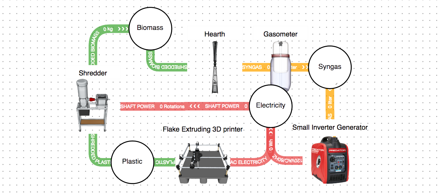
Sam Smith is working on developing a prototype open-source multifunctional waste processing system, named Metabolizer, that mimics the metabolism of a living organism. It is capable of decomposing household wastes in order to power itself as well as provide resources and tools to fabricate its own parts, enabling self-grow, evolve, adapt, and eventually self-replicate. The machine is going to be equipped with a bunch of sensors to monitor its own performance, as well as record and stream the performance data in real-time over the internet.
As per Sam’s design, this system uses heat to decompose shredded waste into a combustible clean gas that can be stored and later be used to feed a lawnmower engine producing shaft power and electricity using a dynamo. The torque from the shaft power can then be used to run a waste shredder, while the so-generated electricity can power the control unit, sensor systems, and a 3D printer that will print out most of its parts from the plastic waste fed to the system. This is an open-source project and Sam aims to provide full documentation and designs for easy replication of this garbage eating self-powered robot by others.
A huge leap in personalized medicine may come from the use of Quantum dots (QDs) to combat and identify several hard to cure diseases, such as cancer, immunodeficiencies, and neurological disorders. Quantum dots (QDs) are semiconductor nanocrystals with unique photophysical properties. Their excellent optical properties are a promising alternative to organic dyes for fluorescence biomedical applications.
In the biomedical sciences, fluorescence is used as a powerful tool for labeling, imaging, and tracking certain molecules or cells. QDs are a new class of fluorophores that offer several improvements over conventional fluorophores. These particles have large absorption and narrow emission spectra, high quantum yield (efficiency of photon emission), long life-time, and high brightness.
Quantum dots for biomedical applications (bioimaging)
When ultraviolet rays hit these dots, they can emit light of different colors based on their size. QDs have useful as fluorescent properties suitable for dyes in the field of deep-tissue imaging. These techniques are typically used in animal models since most organic dyes are not capable of operating in near-infrared (NIR) emissions. The visible wavelength range of about 400-700nm is not suitable for the transmission through biological tissues.
The color of the light depends on the size quantum dot
Specific targeted therapy is delivered to a patient based on particular targeted diagnostic images and tests. Here comes the perfect use for QDs as they can behave as nano-carriers for drug delivery or fluorescent labels. Fluorescent labeling can be explained as the detection involve binding fluorescent dyes to biomolecules to visualize them through fluorescence imaging, such as lymph nodes. This technique makes a great deal in detecting target biomolecules like tumor cells for early diagnosis of cancer, tracking the progress of tumor elimination.
As with every new experimental stage of developing something out of the box, here several challenges stand in the way remain to be solved first it becomes mainstream. There are unknown environmental impact, toxicity, manufacturing costs of these nanomaterials. More research is needed to be done to understand the proper mechanisms and protocols for the scalability of high-quality, non-toxic QD production.
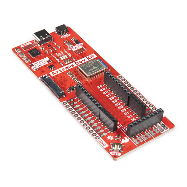
At this point, you may have heard from the Artemis module from Sparkfun, which revolved around the idea of bridging the gap between hobbyists and consumer products, packing all the power that is expected from a modern microcontroller into a small module but keeping in mind the easiness to use and the capability of being ready to the mass-market. Now, with the Artemis Development Kit, you can expect a fully-fledged kit that goes even further than the ones available for this module, allowing access to more software development features than its predecessors. Pretty cool, right?
As a refresher, the Artemis module that brings these kits to life is the world’s first open-source, US manufactured BLE module with FCC, IC, and CE certifications. It runs an Apollo3 ARM Cortex-M4F MCU, supports BLE 5.0, with power as low as 6uA per MHz. This new addition to the Artemis family also includes 24 Breakout I/O pins for your peripherals, a 3-axis accelerometer, a PDM microphone, and optionally a camera, so that you can develop your own computer vision applications on it. It even comes with a useful cheat sheet on the back, detailing all the pin functionalities, so you will not need to go back and forth between your datasheet and your IDE, nice touch!
Regarding the specs in further detail:
Apollo3 ARM Cortex-M4F MCU
1MB Flash + 384KB RAM memories
Built in BLE radio and antenna (48MHz, with 96MHz turbo available)
6uA/MHz, operating at less than 5mW in full operation
Sensors: 3-Axis accelerometer (LIS2DH12) + PDM microphone (SPH0641LM4H-1) + camera connector (for the Himax HM01B0 camera)
Power: 5V provided via USB-C connector, with 1.8, 3.3 and 5V available via the power header
You have flexibility when it comes to programming the kit: as it targets both hobbyists and experienced users who want to take the leap and create a professional product, it allows for the Arduino, but also reccomends some more advanced IDE’s, such as the MBED OS and the AmbiqSDK. The board also counts with an updated USB interface from NXP, providing three different modes: Mass Storage Device (MSD), for drag and drop programming, Human Interface Device (HID), used as the debugging interface to the Artemis module and communication port (COM), providing serial UART communication between the module and the computer connected via USB.
As mentioned by the Sparkfun developers and throughout this article, this board is geared towards the advanced developer, who wants to take a concept all the way into final production. Do you think it can be useful for your ideas? What projects do you see it shining on?
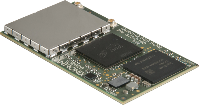
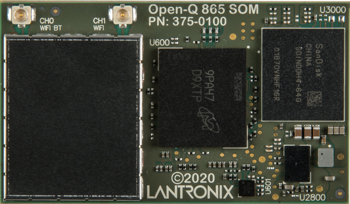
Lantronix Inc. (NASDAQ: LTRX) a global provider of Software as a Service (SaaS), engineering services and hardware for Edge Computing, the Internet of Things (IoT) and Remote Environment Management (REM), today announced its new Open-Q™ 865XR System on Module (SOM) solution for IoT applications. With the Open-Q 865XR SOM, Lantronix is leading the way to next-gen intelligent Augmented Reality/Virtual Reality (AR/VR) applications in AI machine learning, medical, gaming, logistics and retail sectors.
“Our new Open-Q 865XR SOM gives product developers AR/VR capability at the edge, powerful general processing capability and professional-quality imaging needed to kickstart IoT application development,” said Jonathan Shipman, VP of Strategy at Lantronix Inc.
Lantronix’s Open-Q 865XR SOM is an ultra-compact (50mm x 29mm) production-ready SOM powered by the Qualcomm® SXR2130P that utilizes Qualcomm® Technologies’ heterogeneous compute expertise to deliver a System-on-Chip with multiple specialized processing cores, in addition to the Kryo™ 585 Octa-core CPU, including:
5th generation AI engine — twice the performance of the previous generation with up to 15 TOPS
Dual Qualcomm® Spectra 480 ISP — supporting up to 64MP cameras
Qualcomm® Adreno 650 GPU — high performance graphics with power efficiency
Qualcomm® Hexagon 698 DSP — vision processing and machine learning
Adreno 665 VPU — high-quality, ultra HD video encode and decode
In addition, the Open-Q 865XR SOM delivers next-generation wireless and wired connectivity with more reliable performance and higher bandwidth, including:
Wi-Fi 6 — 802.11ax 2×2 MU-MIMO
Two-lane Gen3 PCIe
Two USB3.1 interfaces
Lantronix’s ultra-compact Open-Q 865XR SOM enables product designers to quickly kickstart development for IoT solutions needing advanced technologies at the edge. The Open-Q 865XR delivers on exceptional functionality across many applications, including edge computing, augmented reality, virtual reality, artificial intelligence, machine learning, computer vision and high-resolution input/output. Customer interest is high with initial engagements commencing over gaming, education, medical, logistics and retail applications.
Supported by the fully featured Android™ 10 operating system, the Open-Q 865XR SOM provides the ideal starting point for applications designed to take advantage of the smooth Android UI as well as the advanced camera software stack.
Designed to accelerate time to market for new product innovation, the Open-Q 865XR SOM Development Kit will enable quick, easy evaluation and initial product development. The development kit, along with the available documentation, also provides a functional reference design for custom carrier board development.
“Lantronix’s proven track record of successes with Qualcomm Technologies, including the Open-Q 820 and 845 µSOM products, coupled with Lantronix’s extensive engineering capabilities and services, make us excited to deliver the Open-Q 865XR SOM to new and existing clients,” said Paul Pickle, president and CEO of Lantronix.
In addition to production-ready SOMs, development platforms and tools, Lantronix offers turnkey product development services, driver and application software development and expert technical support.
To learn more about the Open-Q 865XR and download the product brief and datasheet as well as explore all the hardware, software and services Lantronix has to offer, visit www.lantronix.com .
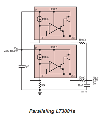
Various configuration of linear regulator for parallel operation discussed in this technical article from Analog Devices.
Linear regulators provide a simple, low noise solution for dc-dc regulation. However, at higher VIN-VOUT differentials the low efficiency and high power dissipation of linear regulators limits the amount of output current that can realistically be delivered. Connecting multiple linear regulators in parallel spreads the load (and the heat) over several ICs, increasing the useful range of output currents a solution can deliver. However, connecting linear regulators in parallel is not always straightforward.
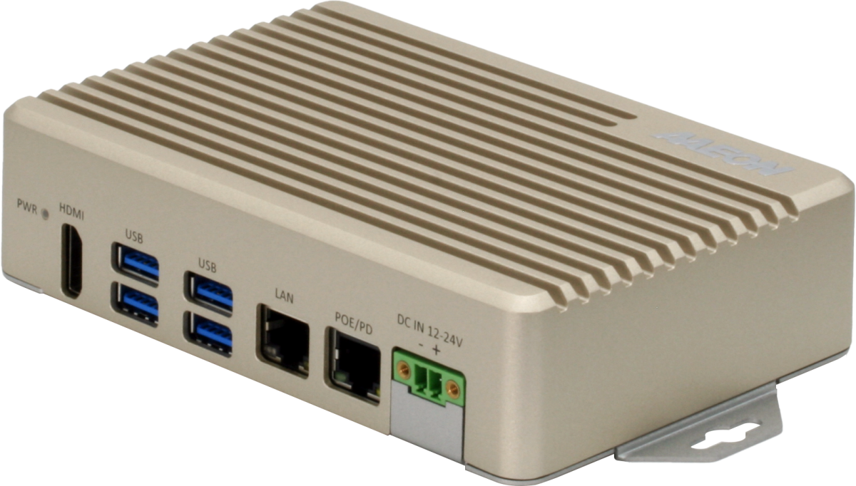
AAEON, an industry leader in AI Edge Computing, announces the BOXER-8222AI compact system powered by NVIDIA® Jetson Nano™. Featuring a PoE PD LAN port, the BOXER-8222AI can be powered by a PSE Gateway allowing for deployment without requiring a dedicated power supply.
The BOXER-8222AI is the latest platform in AAEON’s family of compact rugged AI systems powered by the innovative and energy efficient NVIDIA Jetson Nano SoC. Specialized for AI edge computing, the Jetson Nano utilizes the quad-core ARM® Cortex®-A57 MPCore processor with NVIDIA Maxwell™ GPU architecture featuring 128 NVIDIA CUDA® cores. This innovative design allows processing speeds up to 472 GFLOPs and is capable of operating multiple neural networks or processing several high-resolution images at the same time. The NVIDIA Jetson Nano also features onboard 4GB RAM and MicroSD card slot supporting up to 32GB of storage.
The BOXER-8222AI is unique in its design by featuring a PoE PD (Powered Device) LAN port. This allows for deployment without a dedicated power supply by connecting with a PSE Gateway (Power Supply Equipment). The BOXER-8222AI utilizes the 802.3at standard, supporting power input of 25.6W, more than enough to power the system and connected devices such as USB cameras and sensors.
The BOXER-8222AI also features a flexible I/O loadout including a 40-pin I/O connector designed to support a wide range of sensors and controllers. It also features four USB3.2 Gen 2 ports, RS-232 COM port, as well as LAN, CANBus and HDMI ports. The BOXER-8222AI also supports Wi-Fi expansion with an onboard M.2 2230 slot.
The BOXER-8222AI is designed to operate in a range of rugged environments, featuring a fan-less design to ensure reliable operation. It can operate in temperatures from -10°C up to 70°C without a loss in performance. Its compact size also makes it easy to deploy in tight spaces, putting it closer to where it’s needed.
AAEON offers industry leading service and support with the BOXER-8222AI, from providing technical support to end-to-end solutions to help reduce deployment times and shorten time to market. AAEON also offers manufacturer and OEM/ODM services to help with creating custom configurations, or designing systems from the ground up.
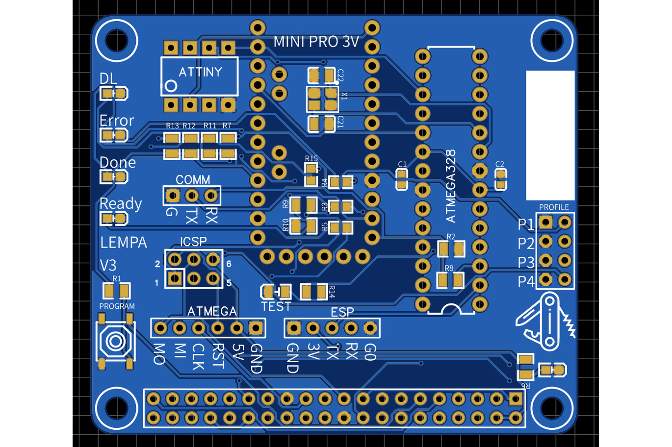
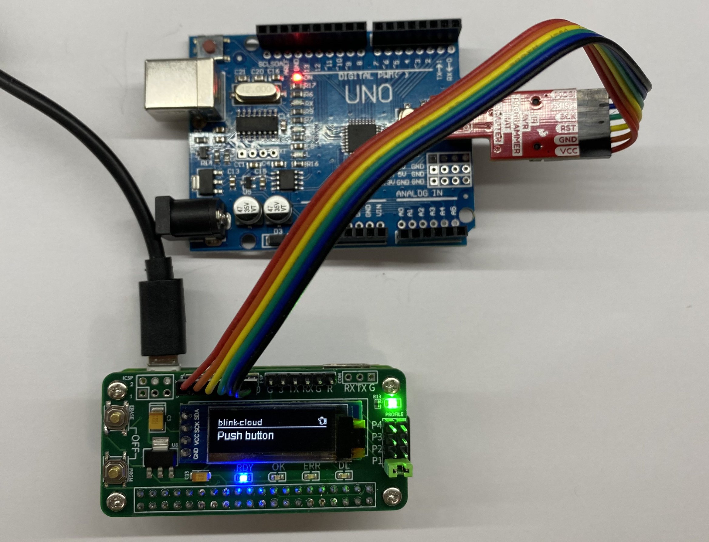
One of the challenges of developing and producing microcontroller-based hardware projects in a repeatable, small/medium volume, is the amount of work it takes to flash the MCUs with the required firmware. Another side of the problem for designers who work with diverse types of microcontrollers is the number of different kinds of programmers they need to have to be able to program the different microcontrollers successfully. Sensing this plight and desiring to provide a better experience for designers, Georgia Based Roey Benamotz’s recently announced the launch of his new integrated MCU programmer called LEMPA.
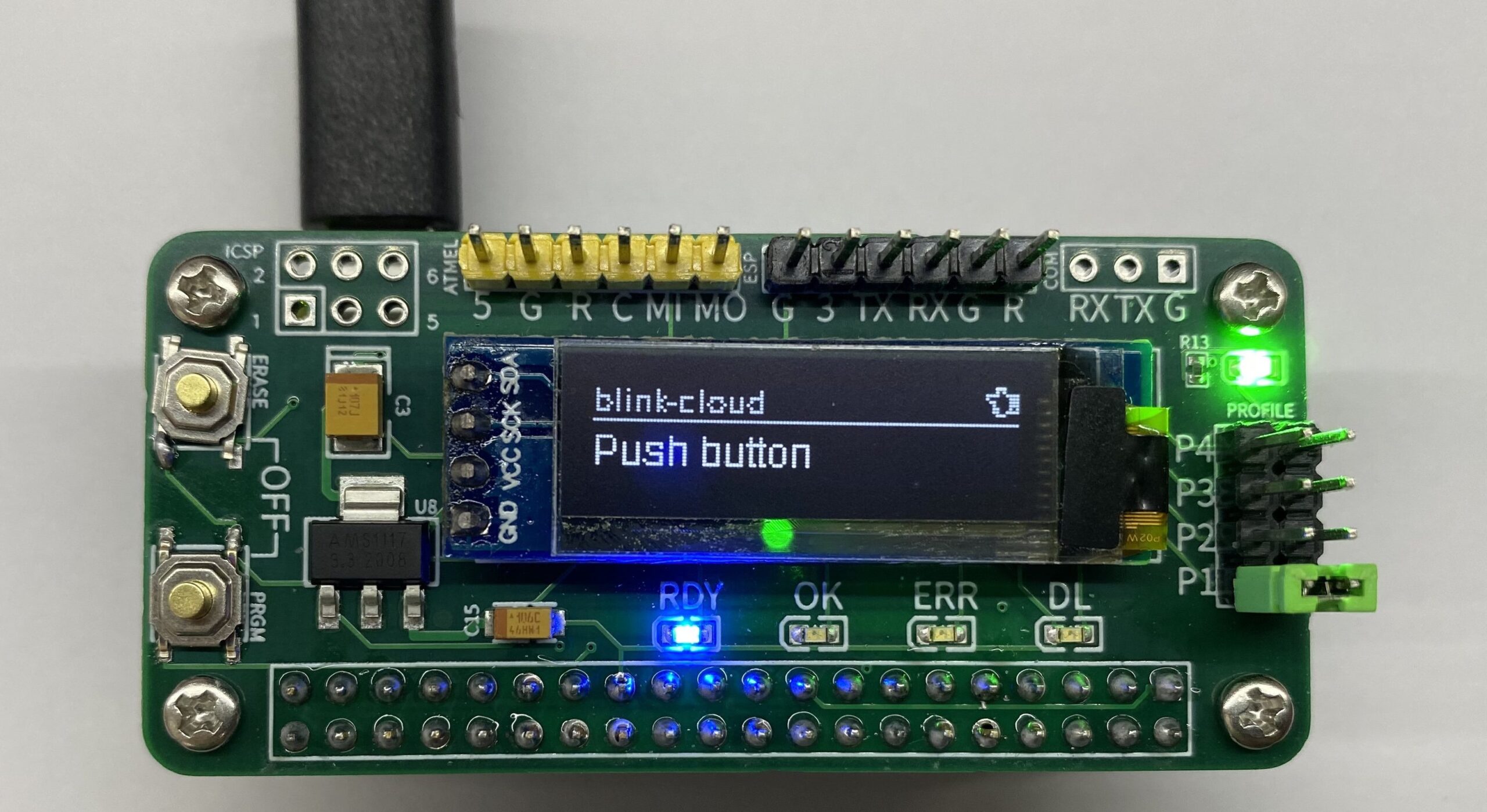
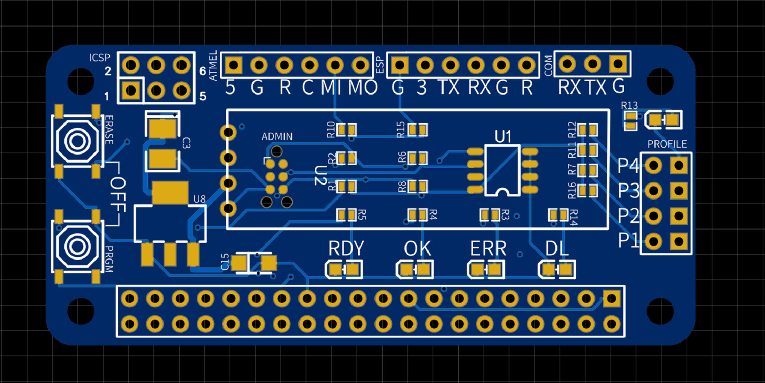
Designed as a Raspberry Pi HAT with the desire for a Pi or other Pin Compatible SBC to serve as the host device, LEMPA provides an easy way for developers to program Microchip Atmega/ATtiny and ESP Microcontrollers with full support for CI/CD and onboard LEDs that provide visual feedback during firmware upload.
The HAT comes with; a ZIF socket to allow for quick insertion and removal of the target DIP-type MCUs, a connector/Socket for ATtiny microcontrollers, and headers for an Arduino Pro Mini dev board. Asides from the LED that provides visual feedback during firmware upload, the board also comes with another LED that can be used to test for the success of the flashing process.
Inline with the goal of the project being to create an integrated tool that enables easy and fast firmware upload, Benamotz also developed a Python-based software that can pull firmware updates from a remote server and handle profile management and flashes the target MCU with the firmware using AVRdude. The software, which runs directly on the Raspberry Pi and other compatible SBCs, makes LEMPA a complete wireless standalone solution without the need for users to connect it to a separate PC to upload firmware, ensuring very little/no wire mess is made.
For repeatability of the firmware upload process, once the setup has been done, to upload firmware, all the user needs to do is to use the jumper on the HAT to select a profile, and press just one button on the HAT to initiate the firmware upload process.
Some highlight features and specification LEMPA(LEan Mean Programming mAchine) include:
Self-contained – no need for PC
Full support for CI/CD – binaries automatically downloaded from cloud or local network
Single-button: One click to program the MCU, long click to download the latest firmware
Support for multiple profiles with the simple editing of a JSON file. A jumper on board chooses which profile to use.
Fully open-source
Does not require cumbersome FTDI adapter or similar
Embedded LEDs provide immediate feedback without the need for a monitor.
While the LEMPA HAT is currently available for sale on Tindie for $19.99, the LEMPA Software is entirely open source and all the code files are available on the project’s Github page here.
More information on LEMPA may be found on the product’s Tindie page which also contains a video that shows how the project works.
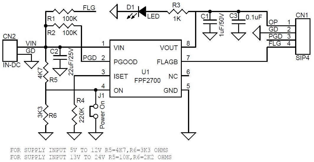
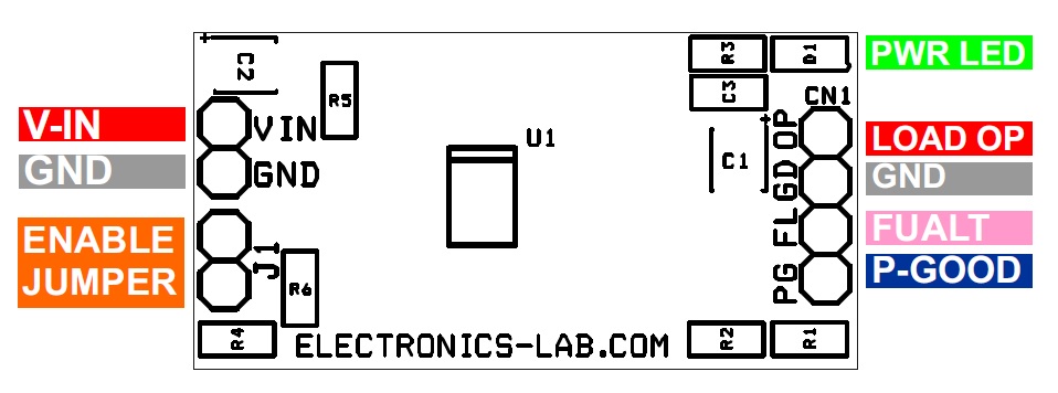
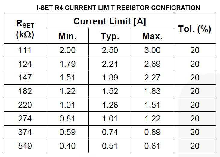
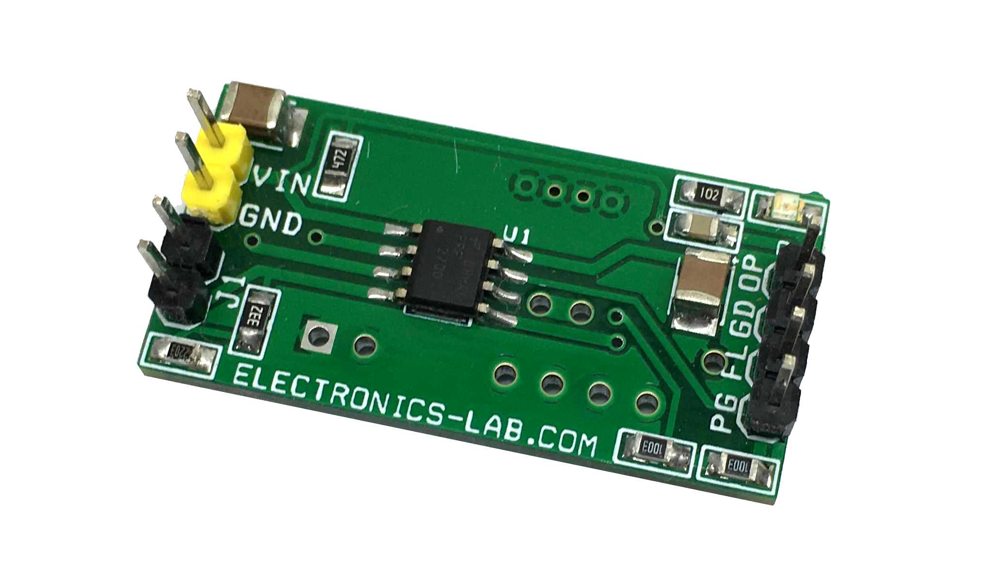
The Over-current limit load switch project presented here provides full protection to devices and loads from access load conditions. The default current limit is set to 1 Amp, however, this load limit is adjustable from 0.4A to 2A with the help of R4 ISET resistor. When an overload condition occurs circuit responds to that overload condition that lasts longer than a fixed blanking period by turning off the load, followed by a retry after the auto-restart time, auto-retry time is 127.5ms. Flag output is pulled up with R1 and the board provides active low output in a fault condition, normally Flag output is high. Power good output is also pulled up and it’s an open-drain output to indicate that the output voltage has reached 90% of the input voltage. The input range of this circuit is 5V to 24V DC. The load can be activated or deactivated with low-voltage logic compatible on Pin4, jumper J1 is provided to activate or deactivate the output. Close the jumper J1 to activate the output load.
An under-voltage condition on the input or if junction temperature is in excess of 140-degree centigrade overrides the ON control and turns OFF the switch. In addition, an over-current condition causes the switch to turn OFF. After the expiration of the blanking time, the IC has an auto-restart feature that automatically turns the switch ON again after the auto-restart time of 127.5ms.
It is important to choose the appropriate value of resistor R5 and R6 which is dependent on the operating power supply, choose R5 4K7 and R6 3K3 for supply input 5V to 12V, alter these resistors value R5 10K and R6 2K2 ohms for supply input 13V to 24V DC. Voltage ON pin 4 should not exceed 5.5V. Default current limit is set to 1A, refer (I-Set resistor R4) table for the current limit set.
The FPF2700 over current limit switch is designed to meet the power requirements of a variety of applications with a wide input voltage range 2.8V to 36V and adjustable current-limit value. while providing optimum operation current for safe designed practices. The core of the switch is a typical 88mOhms (V=12V)
The N channel MOSFET and controller is capable of functioning over an input voltage range of 2.8V to 36V. FPF offers adjustable current limiting, under-voltage lockout, power-good indicator, fault flag output, and thermal shutdown protection. In the event of an over-current condition, the load switch limits the loads to the current value. The current limit value of the switch can be adjusted from 400mA to 2Amps trough the ISET pin. The enable pin is active LOW for and controls the state of the switch. Pulling the ON pin continuously to LOW holds the switch in on state. The switch moves into the OFF state when the ON pin is pulled HIGH. The ON pin can be pulled HIGH to a maximum voltage 5.5V.
Features
Operating Supply 5V to 24V DC
Load Current Limit 1Amps (Adjustable Range 0,4A-2A)
In most of the previous operational amplifier tutorials, the circuits had a feedback loop to the inverting input. This design is the most common because it provides indeed stability and avoids undesirable saturating effects and, it is also common to call it the linear mode.
On the other hand, when no feedback is applied to the inverting input, the op-amp is said to work in the non-linear regime, we can also say in an open-loop configuration. Comparators are specific op-amps circuits that are meant to work in a non-linear mode and can be used as simple logic gates.
A presentation of the circuit along with the basics about comparators is given in the first section.
In the second section, we increase the complexity of the circuit in order to show how to translate the so-called “tipping point” or “threshold” of the comparator. We show that being able to translate this value is important in order to properly design level detectors.
Schmitt triggers are discussed in a third paragraph, we will see how this kind of comparators work and how they can be used in real applications. Moreover, we highlight their advantages by comparing them to basic comparators.
Presentation
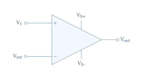
Non-inverting comparator
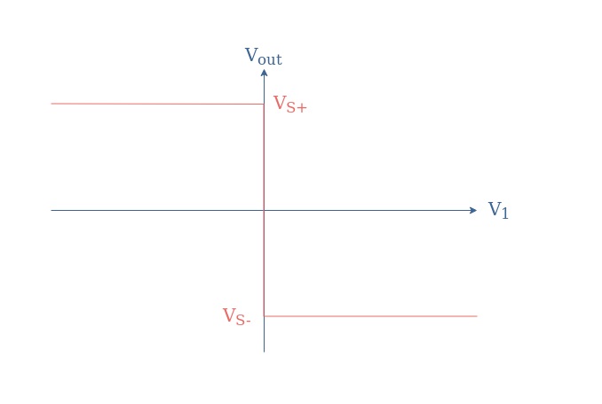
The simplest comparator consists of an op-amp without any resistor or feedback loop, the signal to compare is V1 and supplies the non-inverting input, a reference signal Vref supplies the inverting input, the output is labeled Vout and the supply power is VS+ and VS-, which can be symmetrical or not.
During this presentation section, we will pose and admit that Vref constitutes the ground, and therefore Vref=0. Moreover, we will admit that the supply is symmetrical (VS+=-VS-).
The functioning of this circuit is extremely simple and can be summarized depending on the value of V1:
If V1>Vref, Vout=VS+
If V1<Vref, Vout=VS-
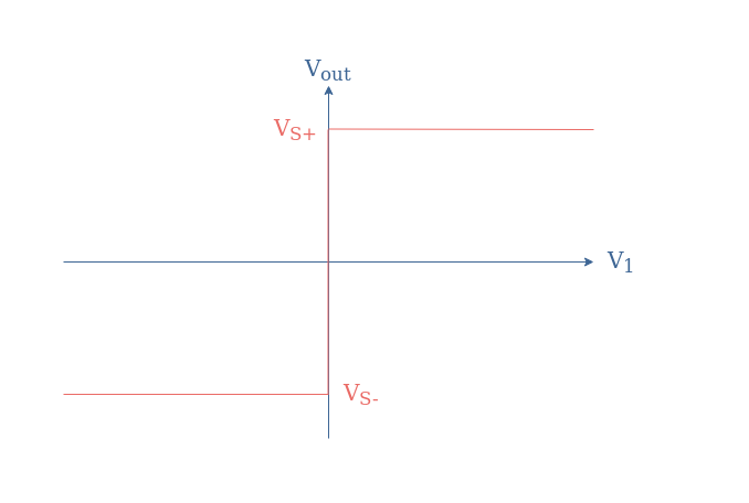
The absence of feedback to the inverting input makes the amplifier to saturate up to the supply power level when the differential input Vin=V1-Vref=V1 becomes slightly higher than zero in absolute value
The input/output characteristic associated with the circuit of Figure 1 is a Heaviside-like function shown in Figure 2 below:
fig 2: Transfer characteristic of the non-inverting comparator
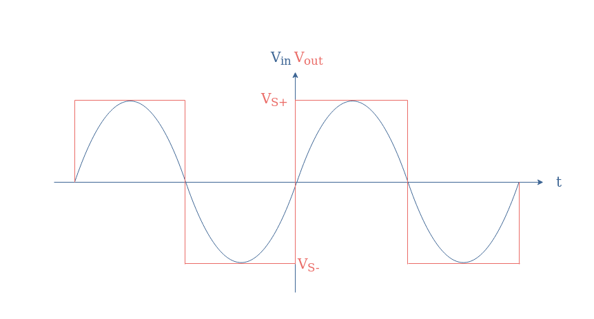
If a sine waveform is applied as an input, the comparator can be used to convert a sine to a square signal:
fig 3: Time-dependent output of a comparator with an input sine
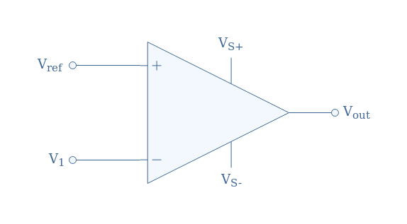
Inverting comparator
In the previous subsection, the signal to compare was applied to the non-inverting input while the reference was on the inverting input of the op-amp. However, the roles can be inverted in order to get an inverting comparator such as presented in Figure 4:
In this case, the value of the output is dictated by these two conditions:
If V1<Vref, Vout=VS+
If V1>Vref, Vout=VS-
The transfer characteristic for this configuration is also a Heaviside-like function but with the positive saturation happening for V1<0 and the negative for V1>0:
fig 5: Transfer characteristic of the inverting comparator
Translation of the tipping point
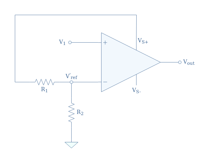
Some complexity can be added with a voltage divider in the reference branch to either the non-inverting or inverting comparator in order to translate the tipping point. The tipping point is the value of V1 for which the output suddenly changes from a high (resp. low) to a low (resp. high) value. In the previous section, the tipping point was always happening for V1=0.
Let’s consider the comparator presented in Figure 6:
fig 6: Non-inverting comparator with a positive tipping point
Thanks to the voltage divider, an alternative reference voltage labeled V’ref is supplied to the inverting input of the op-amp. This new reference satisfies the voltage divider formula: V’ref+=+VS(R2/(R1+R2)). Note that the voltage divider can also be supplied with the negative power supply VS-, in that case, the alternative reference presents a negative sign (we label it V’ref-).
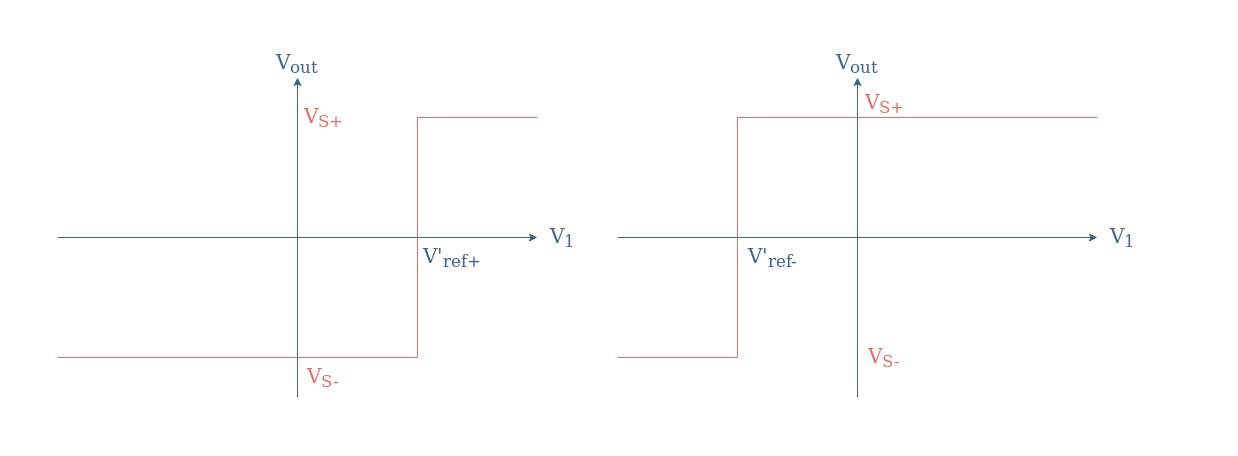
These observations can be summarized in the following transfer characteristics:
fig 7: Transfer characteristics of the non-inverting comparator with positive (left) and negative (right) tipping point
If we consider an inverting comparator, the effect of the same voltage divider circuit will have the opposite effect. Indeed, if the voltage divider is supplied with the positive (resp. negative) power supply, the translation of the tipping point will be negative (resp. positive). Moreover, the signal is inverted such as presented in Figure 5.
Time-dependent input
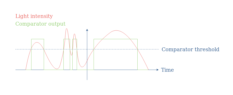
The translation of the tipping point allows setting the threshold level of the comparator to a non zero level. When a variable input is applied to the circuit, such as the output of light or temperature sensor, a simple level detector can be made with this basic comparator.
fig 8: Functioning of a level detector
Schmitt trigger
Non-inverting trigger
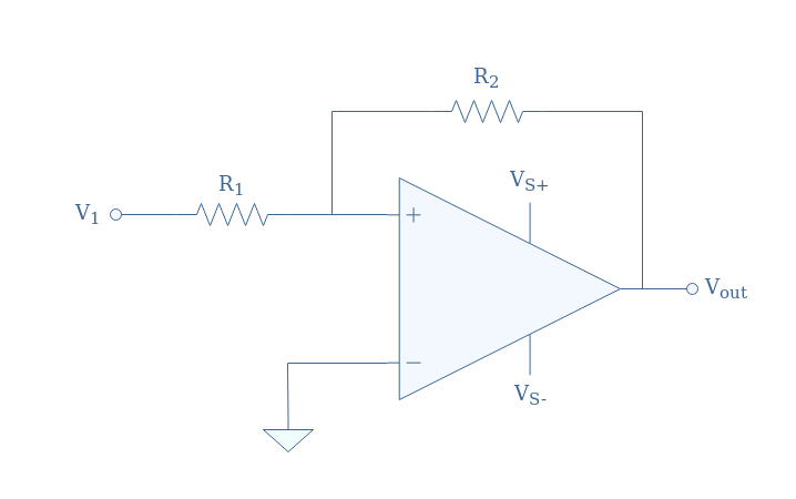
The translation of the tipping point can also be realized by adding a voltage divider circuit as a feedback loop in the non-inverting branch, the inverting branch is grounded (Vref=0). The full configuration is shown in Figure 9 below, it is also known as a Schmitt trigger, we take as an example the non-inverting comparator:
In the situation proposed in Figure 9, the differential input can be written Vin=V+-Vref=V+. Moreover, the voltage V+ can be written as a superposition of V1 and Vout thanks to Millman’s theorem:
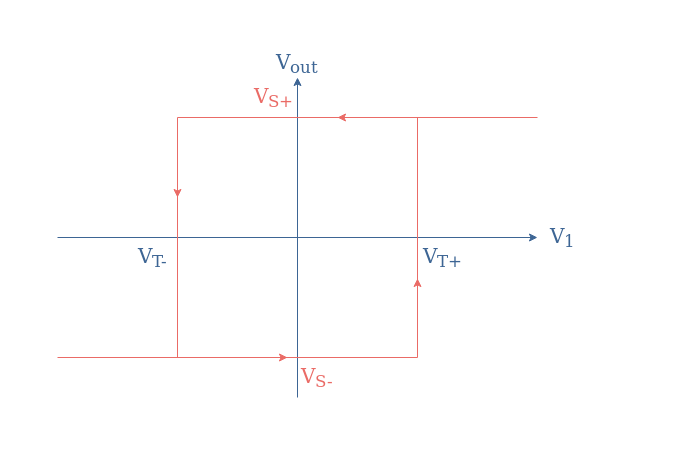
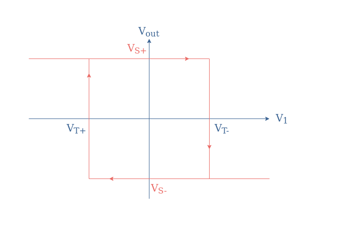
The differential input is equal to zero when V1=-Vout(R1/R2). Since the output value can only be equal to VS or -VS, there are two values of V1 that can be seen as tipping points, we label them VT+ and VT- for “threshold”:
VT+=VS(R1/R2) is the upper threshold for which Vout=VS-→VS+
VT-=-VS(R1/R2) is the lower threshold for which Vout=VS+→VS-
The input/output characteristic of a non-inverting Schmitt trigger is a hysteresis graph presented in Figure 10:
fig 10: Transfer characteristic of the non-inverting Schmitt trigger
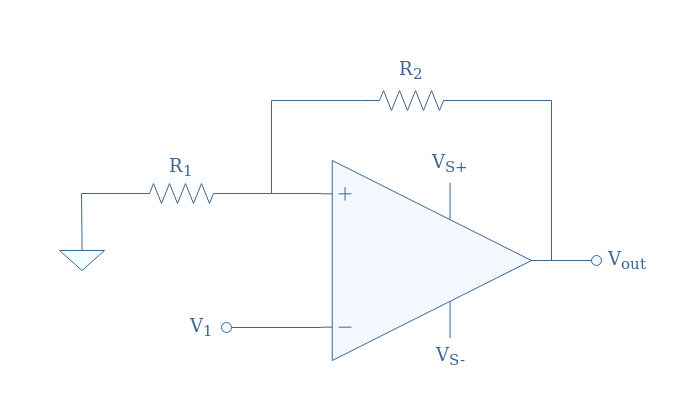
Inverting trigger
We can as well consider the same positive feedback for an inverting configuration:
In this case, the differential input can be written Vin=Vout(R1/(R1+R2))-V1, the input voltage V1 that cancels the differential input is therefore given by V1=-Vout(R1/(R1+R2)).
Depending on the sign of Vout, two thresholds specific to the inverting configuration can be defined:
VT+=-VS(R1/(R1+R2))
VT-=+VS(R1/(R1+R2))
The associated hysteresis plot for the inverting Schmitt trigger is given in Figure 12:
fig 12: Transfer characteristic of the inverting Schmitt trigger
Applications
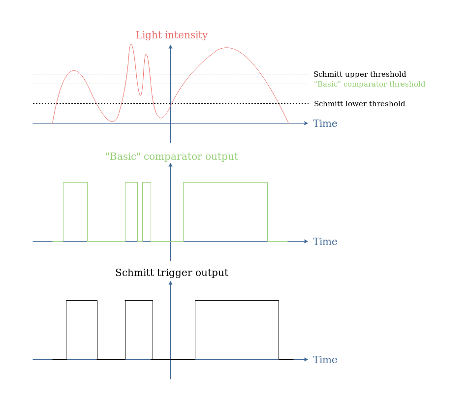
Schmitt triggers and comparators in general, as we briefly presented in Figure 8 are mainly used for the conversion of analogic signals to digital signals.
However, “basic” comparators present the disadvantage of being triggered by background noise. One of the very appreciated properties of Schmitt triggers is their noise immunity, which means that the comparator will switch between the low and high output states only when the input is effectively triggering it. Moreover, since the high output state is triggered by the upper threshold and the low output state by the low threshold, Schmit triggers usually add a delay in comparison with “basic comparators”.
When considering again Figure 8, we could imagine that during the second global light variation, the two peaks can be related to some noise (coming from the user for example).
Thanks to the hysteresis that can be achieved with a Schmitt trigger, if the lower threshold is set below the minimum noise level, the background noise does not trigger the comparator:
fig 13: Comparison of a “basic” comparator and a Schmitt trigger for level detection application
Conclusion
Comparators are operational amplifiers that are intentionally designed to work in open-loop or with positive feedback, which is both unstable and non-linear modes. Their output can only be equal to two different values, which correspond approximately to the power supply voltages. The output, or saturating voltages, depending on the input supplied. This input is being compared to a reference voltage which sets the threshold of the comparator.
In the second section, we have seen that the threshold voltage can be modified by adding a simple voltage divider circuit to the inverting branch of the op-amp. Basic comparators work in open-loop and present only one threshold, which makes them simple to design and with a fast response.
The third section focuses on Schmitt triggers which present the advantage to not be triggered by background noise, such as basic comparator do. Schmitt triggers do not work in open-loop configuration but instead with positive feedback to their non-inverting input. It allows them to have two threshold levels (high and low), as a consequence, their transfer characteristic is a hysteresis.
The EE895 sensor module is ideal for use in climate measuring devices. Pressure and temperature compensation ensure a high CO2 measuring accuracy.
The new EE895 sensor module from E+E Elektronik measures CO2, temperature and ambient pressure. The small 3-in-1 module is an ideal choice for measuring instruments used for ventilation and climate control, in building automation or for process control. Due to its low power consumption, the module is also suitable for battery-operated devices such as hand-held meters, data loggers or wireless transmitters. The temperature and pressure compensation ensures high CO2 measurement accuracy under changing environmental conditions.
A Single Module – 3 Measurands
Additionally to CO2 concentration up to 10 000 ppm the EE895 module measures also the temperature and ambient pressure. The pressure and temperature compensation with on-board sensors minimizes the environmental influences onto the CO2 measurement. Thus the module offers a constantly high CO2 measurement accuracy, independent of altitude or changing ambient conditions.
Long-Term Stable CO2 Measurement Principle
The dual wavelength NDIR CO2 measuring principle with auto-calibration ensures long-term stable measurements, as it automatically compensates for aging effects and is particularly resistant to contamination. The factory multi-point CO2 and temperature adjustment procedure leads to an excellent CO2 measurement accuracy over the entire temperature working range of -40…60 °C (-40…140 °F).
Easy Design-In
The measured data for CO2, temperature and pressure is available on the I2C or UART interface. The very small dimensions of only 35 mm x 15 mm x 7 mm (1.38″ x 0.6″ x 0.27″) and various mounting options facilitate the design-in of the sensor module.
Flexibly Configurable
The EE895 module can be flexibly configured via the digital interface. The CO2 measurement interval can be set according to the application and the power requirements.
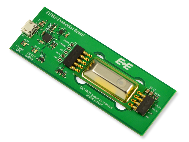
Evaluation Board for Testing on a PC
With the separately available EE895 Evaluation Board, the sensor module can be tested on a PC. The free evaluation software displays the measurement data in graphical form and allows the user to set the sampling rate and the measurement units for temperature and pressure. For further processing, the data can be saved as .CSV file.