TCA4307 Hot-Swappable I2C Bus and SMBus Buffer

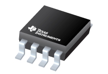
Texas Instruments’ buffer features stuck bus recovery

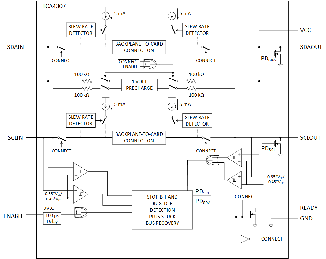
Texas Instruments’ TCA4307 is a hot-swappable I2C bus buffer that supports I/O card insertion into a live backplane without corruption of the data and clock lines. Control circuitry prevents the backplane-side I2C lines (in) from being connected to the card-side I2C lines (out) until a stop command or bus idle condition occurs on the backplane without bus contention on the card. When the connection is made, this device provides bidirectional buffering, keeping the backplane and card capacitances isolated. During insertion, the SDA and SCL lines are pre-charged to 1 V to minimize the current required to charge the parasitic capacitance of the device.

The TCA4307 has stuck bus recovery, which automatically disconnects the bus if it detects either SDAOUT or SCLOUT are low for about 40 ms. Once the bus is disconnected, the device automatically generates up to 16 pulses on SCLOUT to attempt to reset the device which is holding the bus low. When the I2C bus is idle, the TCA4307 can be put into shutdown mode by setting the EN-pin low, reducing power consumption. When EN is pulled high, the TCA4307 resumes normal operation. This buffer includes an open-drain READY output pin, which indicates that the backplane and card sides are connected. When READY is high, the SDAIN and SCLIN are connected to SDAOUT and SCLOUT. When the two sides are disconnected, READY is low.

  • Supports bidirectional data transfer of I2C bus signals
  • Operating power supply voltage range: 2.3 V to 5.5 V
  • Ambient air temperature range (TA): -40°C to +125°C
  • Stuck bus recovery featuring automatic bus recovery
  • 1 V pre-charge on all SDA and SCL lines prevents corruption during live insertion
  • Accommodates standard-mode and fast-mode I2C devices
  • Supports clock stretching, arbitration, and synchronization
  • Powered-off high-impedance I2C pins

more information: https://www.ti.com/product/TCA4307

Water Contact Indicator Tape

Water Contact Indicator Tape from 3M™ changes color with water contact without performance degradation in high humidity exposure

3M™ Water Contact Indicator Tape is a tape that changes color from white to red upon contact with water. It is designed to withstand heat and humidity aging without giving water indications. The tape permanently changes from white to red upon direct water contact. In electronic products ranging from mobile phones, 2-way radios, video cameras, laptops, and Li-MH batteries/chargers to electrical box enclosures, users will have clear evidence of water contact without false identification from high humidity.

  • Highly absorbent, paper backing to transport water to show indication
  • Does not falsely indicate water contact in high humidity exposures
  • Performance not degraded by high humidity exposure
  • Printable top layer by thermal transfer, flexographic, or screen-printing methods
  • Easily die cuttable with rotary die-cutting process
  • Very high bond strength adhesive to most surfaces, including low surface energy plastics
  • UL-969 compliant
  •  Thickness:
    • 5557 Series: 0.0102″ (10.2 mils, 0.259 mm)
    • 5558 Series: 0.0060″ (6.0 mils, 0.152 mm)
    • 5559 Series: 0.0050″ (5.0 mils, 0.127 mm)

more information: https://www.3m.com

Jake Wachlin Demonstrates His CAN Controlled Dual Closed- Loop Motor Controller

Jake Wachlin has posted on Hackaday a CAN Controlled Dual Closed-Loop Motor Controller. CAN is an acronym for Controller Area Network. This is a robotic vehicle bus standard designed to enable microcontrollers and devices to communicate with each other’s applications without a host computer. This mechanism is implemented in the CAN controlled dual closed-loop motor controller. This controlled dual closed-loop motor controller can be used for a SCARA robot, control a leg of a robot, and versatile if needed for any motor control. About the project, Jake says “This project aims to develop a low-cost design which can be used for closed-loop control of two micro-gear motors. The current to the motors will also be monitored for current limiting and possible impedance control applications. It can be interfaced over CAN bus, ensuring robustness and scalability in robotics applications.”

The PCB Layout

During the course of the project, CAN interface didn’t work with the V1.0 dual controller, however, Jake says that a V1.1 update should improve the workings of the controller. Also, the use of JLCPCB as an assembly service and EasyEDA for its clean interface is part of the changes made amongst the following :

  • Add a 16MHz crystal to the MCP2515 to fix the CAN issue
  • Add pads at logic level CAN TX/RX for debugging support
  • Label all external connections on the silkscreen
  • Label maximum input voltage
  • Add optional CAN 120 Ohm termination resistor with a solder jumper
  • Add 3-bit device numbering with solder jumpers to address devices without firmware changes
  • The first version just used 0.1″ pitch through holes for the motor and power/CAN connections. On V1.1 I chose actual screw terminal connections so wires don’t need to be soldered permanently in
  • Add holes that can be used for mounting
  • Add bulk capacitance for the motor controller (doesn’t seem strictly necessary, but not a bad idea to have).
  • The assembly service supports a limited number of components and only single-sided SMD parts so are preferable if the assembling can be done personally.

These dual motor controllers are meant to be peripherals on a larger network. They receive higher-level commands from some external device over CAN, and handle the low-level motor control, therefore building a simple main controller is advisable. The main requirements are an attitude sensor and sufficient computational capability to theoretically run complex walking gait controllers. The ESP32 with 2 cores at 240MHz is used because of its computational capability to run fairly complex control schemes that have a built-in CAN controller. It also supports wireless connectivity so commands can be sent remotely.

With the project now able to control two motors well, and much of the supporting code for more complicated use cases written, the next step is to set up the communication between devices. For this, the Controller Area Network (CAN) bus is used. Originally developed for automotive use, CAN allows for relatively high-speed, robust, and long-range multi-master communication. It uses two wires which are differentially driven by a dedicated transceiver. Preferably use the TCAN334. While some microcontrollers have a CAN controller built-in, the ATSAMD21 does not, so use the ubiquitous MCP2515. The MCP2515 is commonly used in all sorts of low-cost hobbyist (and serious commercial) CAN applications. It has an SPI interface to the ATSAMD21.

More information about the controller can be found on Jake’s project page on Hackaday.

Adafruit BrainCraft HAT – Machine Learning for Raspberry Pi 4

Think about what would be useful when developing your machine learning projects for the Raspberry Pi, maybe a camera, a display, some input and output sound capabilities or even an easy means to easily inject the results of your algorithms into servo motors or other devices. Look no further, as the BrainCraft HAT gives you everything you need to kickstart your machine learning on the Raspberry Pi!

The BrainCraft HAT is Adafruit’s take on how you would like to make machine learning projects for the Raspberry Pi, making it easy for you on the development stage. Their inspiration came when they picked up some popular projects on TensorFlow and realized what would be handy to have in each of them. For example, in computer vision projects, how annoying it was not to have a visual representation of what is happening. There is also a slot for a camera, a joystick, buttons, microphones for your audio recognition projects (which can be mechanically powered off, something Alexa and other home assistants should take into consideration) and some extra connectors where you can easily plug relays, servo motors and other electronics, which is something you do not see a lot and extremely useful, bringing the gap between actuators and machine learning even closer. Lastly, as this is a HAT, you can still access you Raspberry Pi pins.

Regarding the specs:

  • 240×240 1.54’’ IPS TFT display;
  • Stereo speaker output (1W) + stereo headphone output;
  • Stereo microphone input (with an On/Off switch that completely disables the audio codec);
  • 2x 3-Pin JST STEMMA connectors on PWM pins + 1x STEMMA QT plug-and-play I2C port (can be used to connect objects such as heat sensitive cameras);
  • 5-Way Joystick + Button for user interface and control;
  • 3x RGB DotStar LED’s for colorful feedback;
  • Controllable mini fan on the bottom to cool your Raspberry Pi.

The HAT’s performance is very acceptable, by looking at the introductory video on their website. They showcased an object identification project directly on the Raspberry Pi 4, packed with the TensorFlow Lite, while displaying video from the camera on the display and everything worked seamlessly. Interestingly, the performance only started to dip when the fan was turned off, typical of the Raspberry Pi 4.

Regarding the state of the BrainCraft HAT, it was just released and almost immediately stocked out, showing it already is taking off in the maker industry! Don’t worry, you can get notified via email when it gets stocked back. At a price of $39.95, you get a lot of value.

What do you think? Is it something you’ll consider pick up? I certainly think is worth your time.

Adafruit BrainCraft HAT Link: https://www.adafruit.com/product/4374

STWIN SensorTile Wireless Industrial Node development kit and reference design for industrial IoT applications

What is not to love about aggregating boards? They ease the development process, giving you a necessary time boost because you have a board with some of the components you may need right there, ready to be used in your new application! This is why you need to take a look at the STWIN SensorTile.

But what exactly is the SensorTile? As you may have guessed by the name, it is a development kit that features a wide range of industrial-grade sensors, developed to simplify the prototyping and testing of some advanced IoT applications, such as condition monitoring and predictive maintenance. In this development kit, you can find sensors ranging from a 3D accelerometer to a MEMS motion sensor, paired with a low power microcontroller from ST and even connectivity options, granted by an on-board BLE module and other options, such as Wi-Fi (through an external expansion board) or even RS485 serial communication. The kit also includes an STMod+ connector, to which you can connect other small, compatible and low-cost ST daughter cards and contains a 480mAh Li-Po battery, a ST-Link debugger and a plastic enclosure.

Looking closely to the specs of this sensing beast:

  • Ultra low power ARM Cortex-M4 MCU (120MHz with FPU, 2048kbytes of Flash memory)
  • MicroSD card slot
  • On-board Bluetooth Low Energy 4.2 (BLE) module and Wi-Fi available through expansion board + RS485 and USB OTG wired connectivity
  • Sensors: Ultra-wide bandwidth, low noise, 3-axis digital vibration sensor, 3D accelerometer + 3D gyroscope with machine learning core, ultra-low-power MEMS motion sensor + 3-axis magnetometer, digital absolute pressure sensor, relative humidity and pressure sensor, low-voltage digital local temperature sensor and industrial grade + wideband analog MEMS microphones
  • Modular architecture, with STMOD+ and 40-pin expansions + 12-pin connectivity expansion + 12-pin sensing expansion
  • 480mAh Li-Po battery
  • STLINK-V3MINI debugger
  • Plastic enclosure
System block diagram of the STWIN SensorTile

Regarding the software, you are greeted with an interesting set of packages and optimized libraries, as well as a cloud dashboard application, ready to help you speed up your next development cycle. And if you ever worked with ST microcontrollers before, you know how easily you can set up new projects on the STM32CubeMX software. Lastly, it also is an AWS qualified device, meaning it works with the AWS IoT core, FreeRTOS and other AWS tools.

Right now, you may be wondering: this thing isn’t cheap. Well, by the value you are getting through the number of components by squared inch. This board has practically everything you need to get started on a wide range of projects, and it comes at a cost of only $98.

What do you think about this kit? Will it be a part of your next IoT development cycle? It certainly has the potential to do so!

STWIN SensorTile link: https://www.st.com/en/evaluation-tools/steval-stwinkt1.html?icmp=tt14874_gl_bn_apr2020#overview

iWave Launches Industry Latest High-End FPGA SOM Based on Arria 10 GX FPGA

iWave Systems, a global leader in the design and manufacture of cutting edge FPGA solutions, is launching a new System on module based on the powerful Intel Arria 10 FPGA GX devices. The Arria 10 FPGA SOM is power-packed with up to 1150K Logic Elements, duel DDR4 RAM with 64 bit and 32-bit storage capabilities. A wealth of high speed I/Os and interfaces that enable the module to fulfill complex data integrity requirements while ensuring faster throughput, reduced latency, and low power execution, accelerating the development of FPGA-based applications in industrial, aerospace, and medical domains.

The SOM is designed to help developers and OEMs with a powerful and well-integrated FPGA platform that help reduce design cycles and accelerate innovations in applications such as “Test and measurement equipment, Control and intelligence equipment, Diagnostic medical imaging equipment, Wireless infrastructure equipment, RADAR, Automation and Military applications.”

At the heart of the Arria 10 FPGA module from iWave is the Intel Arria 10 GX FPGA, which features 20 nm technology on an F34 package. The module supports seven GX models — GX270, GX320, GX480, GX570, GX660, GX900, and GX1150 which provide varying levels of FPGA logic elements (LEs) ranging from 270K to 1150K, offering a range of options for customers to select the best fit FPGA that serves their applications.

With 500MHz logic core performance, the GX models support 24 transceiver lanes and run on up to 40 per cent lower power, which guarantees data integrity and high performance in power and resource-constrained applications. Up to 189 user I/Os and 24 multi-gigabit transceivers each offering a data transfer rate of up to 17.4 Gbit/sec is available on two 240 pin high-speed board to board connectors.

The module can support interfaces like PCIe Gen3 x8, SATA Gigabit Ethernet, USB3.0, etc providing a range of flexible options that help customers towards various use cases. The module’s up to 4 GByte large DDR4 SDRAM facilitates faster throughput and an ultra-low latency data path for real-time executions.

For quick prototyping and time to market, iWave supports a development platform, which includes a powerful configuration of the Arria 10 FPGA SOM with a custom form factor carrier board. Arria10 FPGA Development board supports a wide range of high-speed interfaces like Dual FMC (HPC) Connectors, M.2 SATA, 10G SFP+, 3G/12G SDI In & Out, USB 3.0 TypeC connector and, one PCIe connector to validate Arria10 FPGA high-speed transceivers and other on-board connectors to validate the Arria10 FPGA I/Os. The LPC/HPC FMC connectors provide expansion options on the carrier board, which is compatible with a wide range of plug-in cards such as ADCs, DACs, motor control cards, RF links, etc.

iWave provides full product design engineering and manufacturing services around the Arria 10 FPGA SOMs to help customers quickly develop innovative products and solutions. iWave also offers a comprehensive ecosystem for the Arria 10 FPGA SOM, offering all of the hardware, software, and support materials making it easy to jump-start application development using the Arria 10 GX FPGA.

For further information or enquiries please write to mktg@iwavesystems.com

AAEON: Next Generation Embedded Solutions Powered by Intel Technology

AAEON, a leader in embedded solutions, announces up-coming products featuring the 11th Generation Intel Core processors (formerly Tiger Lake) and Intel Atom x6000E series processors, Intel Pentium and Celeron N and J series processors (formerly Elkhart Lake). These next-generation solutions provide greater performance, flexibility and a host of Intel technologies to power computing at the edge.

The 11th Generation Intel Core processors, now the third generation of Intel’s 10nm microarchitecture, provide performance above the current industry standard 8th and 9th Generation processors. These processors also open up access to cutting edge technologies, featuring the Intel Iris Xe graphics (Gen 12), PCIe 4.0, Thunderbolt 4, USB4, DDR4 and LPDDR4x memory, and Deep Learning Boost on select SKUs.

AAEON brings the 11th Generation Intel Core processors in several key embedded form factors, with the PICO-TGU4, GENE-TGU6, and COM-TGUC6. These boards are designed to provide performance and flexibility on a range of compact form factors designed to make installation and deployment quick and easy. With industrial-grade construction, AAEON’s embedded boards offer stable and reliable performance no matter where they’re deployed. AAEON will also bring the 11th Generation Intel Core processors to the UP Board line up with the UP Xtreme i11 (UPX-TGL01), providing makers and independent developers access to this new generation of Intel processors.

AAEON also has two new products coming soon, based on the Intel Atom x6000E series processors and Intel Pentium and Celeron N and J series processors. The PICO-EHL4 brings these efficient processors to the PICO-ITX form factor, along with a strong compliment of I/O features, including four USB3.2 Gen 2 ports, two HDMI ports, and two Gigabit Ethernet LAN ports. AAEON will also bring this family of Intel processors to the UP Board line up with the UP Squared Pro 2 (UPN-EHL01), featuring M.2 3042/3052 slot designed for 4G and 5G support.

“With the release of these two families of Intel processors, AAEON will provide developers and users with a broader range of products to power applications from kiosks and digital displays, to edge computing IoT networks and AI applications,” said Kevin Chiu, Vice President of AAEON’s Embedded Computing Division. “Thanks to our partnership and working closely with Intel, we look forward to providing cutting edge solutions to our customers, and expanding our lineup of products featuring these innovative processors,” Kevin Chiu added. “AAEON will also sell the Intel Customer Reference Board for Intel Pentium and Celeron N and J series processors through our eShop.”

“The new Intel Atom x6000E series processor and Intel Pentium and Celeron series processor demonstrate Intel’s commitment to our customers by delivering an IoT centric, highly integrated processor that can handle a variety of workloads, form factors and use conditions. This allows AAEON to enable next-generation performance and new capabilities across their broad portfolio of products,” said Mandy Mock, Vice President of IOT Platform Management, Intel.

AAEON will release these platforms over the coming months and continue to expand its lineup of embedded solutions. For more information about these products, visit AAEON’s website or contact an AAEON sales representative.

Geniatech XPI 3128 RK3128 SBC is Equipped with an NXP WIFi 5 Module

Your first reaction to the Geniatech XPI 3128 SBC may be “I have seen this somewhere… Is this related to the Raspberry Pi 3?”, and you are right, the board is strikingly similar to the ever-so-popular Raspberry Pi, but do not let the looks deceive you!

The XPI 3128 is the new addition to the Geniatech‘s family of SBC’s, and this board fits into the cheap media player category, bringing some features you would expect in one, such as an IR receiver, Full HD 60 fps HDMI output, Wi-Fi 5 connectivity, among other things, while also providing decent processing and graphical capabilities, such as HEVC hardware, supporting H.265 decoding. Of course, we can’t shake the similarity between this board and the Raspberry, but its premise seems slightly different.

Regarding its specs, we are looking at:

  • Rockchip RK3128 ARM Cortex-A7 processor (quad core, clocked up to 1.2GHz)
  • ARM Mali 400 MP2 GPU
  • 1GB (2GB optional) DDR3L and 8GB (16/32/64GB optional) EMMC Flash internal memories, expandable through a MicroSD card slot
  • HDMI video output up to 1080p/60fps + H.264/H265 video decoding
  • 4x USB 2.0 ports (one with OTG support) + 1x Micro USB port + 1 ethernet connector
  • 40-pin GPIO header compatible with Raspberry Pi (access for UART, I2S, PCM, I2C, GPIO, PWM, …) + 4-pin pitch header for serial console
  • 802.11 a/b/g/n/ac 2.4GHz/5.8GHz Wi-Fi and Bluetooth 4.0 connectivity
  • IR receiver
  • 12V/3A power supply, standby mode <0.5W
A look to the side of the board. Shouldn't the IR receiver be located on the other side?
A look to the side of the XPI 3128 board and its hardware

From a hardware standpoint, you are not very limited, as the connectivity is what is expected from media players and you also have some expandability options. One thing worth noting is that the step towards 4k was not given, limiting the content streaming capabilities on higher-end televisions. This can be an advantage if the product is not priced accordingly. To this date, there is no information on pricing, but the XPI 3128 is expected to become available soon on Geniatech’s shop.

Regarding the software possibilities, you can count on the support for Linux and Android 7.1, arguably the most popular OS’s used in media players nowadays, so it’s aligned with our expectations.

When considering possible competitors, there is not a lot that can differentiate this board from others on the market, aside from the connectivity, as there are already similar boards when it comes to specs and located at a fairly decent price tag. We will have to wait and see how this board performs on the market, but I’m missing a more differentiating factor here.

What do you think? Will you pick it up as your next media player, or were you expecting something more? We would love to hear your opinion in the comments section.

Fifth gen Banana Pi (Banana Pi BPI-M5) is on the verge

SinoVoip has listed specs for an upcoming Banana Pi BPI-M5 SBC with the same quad-core Cortex-A55 Amlogic S905X3 SoC. It is repeating many of the features from Hardkernel’s $50 Odroid-C4. This new SBC is the next-gen for the company’s most recent Banana Pi BPI-M4, based on a quad A53 Realtek RTD1395.

The 12nm fabricated Amlogic S905X3 is equipped with 4x, up to 2GHz Cortex-A55 cores, and a Mali-G31 GPU. As mentioned earlier, this board is similar to the Odroid-C4, is an open-spec, Raspberry Pi style board. It comes with 40-pin GPIO, 4GB LPDDR4, and support for Android and Linux. Other common features include 4x USB 3.0 host ports, a MicroSD slot, a GbE port, an HDMI 2.0 port with 4K@60Hz support.

Other misc I/O ports are listed as audio jack, IR, serial debug, and a USB Type-C port for 5V power. With the dimension of 92 x 60 mm we can conclude that this SBC is a bit larger than the Odroid-C4 or even Raspberry Pi. It is unfortunate to see that BPI-M5 lacks the support for the M.2 slot. PoE, and built-in WiFi/Bluetooth whereas the previous generation, BPI-M4 include them.

Banana Pi BPI-M5

Hardware spec for the Banana Pi BPI-M5 :

  • Processor: Amlogic S905X3 (4x Cortex-A55 @ up to 2GHz)
  • GPU: Mali-G31 GPU @ up to 650MHz
  • Memory: 4GB LPDDR4 RAM
  • Storage : 16GB eMMC with optional up to 64GB, MicroSD Slot
  • Networking: 10/100/1000 Mbit/s Ethernet
  • Media I/O: HDMI 2.0 port for up to 4K@60Hz with HDR, CEC, EDID, 3.5mm audio jack
  • Other I/O: 4x USB 3.0 host ports, USB Type-C port for power, Serial debug header, 40-pin GPIO header (UART, I2C, SPI or PWM, 5V, 3.3V, GND, 28x GPIO)
  • Power: 5V DC via Type-C; power, reset, and boot switches
  • Dimensions & Weight : 92x60mm, 48g
  • OS Support: Android, Linux

The company says it will provide Android and Linux images with source code. We’ll have to keep an eye on pricing once the board comes out. Further information can be obtained from the company’s wiki page.

Mobile, Open-Hardware, RISC-V System-on-Chip (SoC) Development Kit

By looking at the Precursor you may wonder “Are we not through with these phones yet?”, but who said this was a regular phone? Its deceiving looks hide an open hardware development platform for mobile communication and computation in a secure environment. Intrigued?

The Precursor is described by the developers as a device for everyday use that compromises nothing as a development platform. It is powered by an FPGA-hosted, soft-core System-on-Chip (SoC), giving the developers a lot of freedom when it comes to the customization of the platform, but it doesn’t end there. It was designed from the ground up with one main goal: security. It can be considered a strong starting point for your projects. The developers describe some interesting things you can apply with the platform:

  • Secure communication – With an easier-to-verify hardware design, self-provisioning and support for modern crypo primitives, you are in for a treat if secure communication is what you’re looking for! It uses the Silicon Labs WF200 for Wi-Fi connectivity and contains a headphone jack, allowing for end-to-end encrypted voice communications.
  • Key protection – Its security characteristics make it particularly interesting when it comes to developing two-factor authentication solutions, crypto wallets and other critical applications. Since supply chain attacks are devastating in these cost-conservative targets, you may consider building your own SoC and firmware from the ground up to limit the attacking surface, where the Percursor was conceived to ease this process.
  • CPU emulation – Even though its FPGA ships with a 32-bit RISC-V CPU, you can easily configure it to emulate a comprehensive library of retro CPUs, such as the 6502 from the NES or the Z-80. You can even turn it into a retro pocket-sized console with some creativity!
The Precursor's hackable hardware
The Precursor’s hackable hardware

Regarding some of the specs of the system:

  • Xilinx XC7S50 primary System on Chip (SoC) FPGA (-L1 speed grade for longer battery life) + iCE40UP5K secondary Embedded Controller (EC) FPGA (manages the power, standby and charging)
  • 16MB external SRAM + 128MB Flash memories
  • Dual hardware TRNG
  • Physical keyboard (modular keyboard PCB, customizable to add sensors or swap for touch surface), black and white LCD (200ppi, 226×536 resolution)
  • Audio: Integrated 0.7W speaker, vibration motor and headset jack
  • Integrated Wi-Fi (hardware-sandboxed WF200C chipset)
  • USB type C port + 1100maH battery
  • Anti-tamper features

Its small form factor, quite similar a phone from the 2000’s, accomodates a built-in display, a physical keyboard and an internal battery on the inside, while remaining lighter than the average smartphone. But don’t get deceived by its looks, as it provides hooks for harware modifications, where the keyboard is an I2C-based PCB and the battery cavity exposes GPIO pins, allowing you to swap battery life for extra hardware functionalities. Every bit of the Percursor is hackable, including the mainboard, daughtercards and case, the SoC implementation and firmware, the secondary embedded controller and even an OS that is on the works.

The project will be available soon on Crowd Supply, where you can get an even more detailed view over the Percursor, including a full hardware spec list. Which project do you see the Precursor shine on?

Precursor Crowd Supply Link: https://www.crowdsupply.com/sutajio-kosagi/precursor

TOP PCB Companies