MUSTOOL G1200 Microscope Quick Review

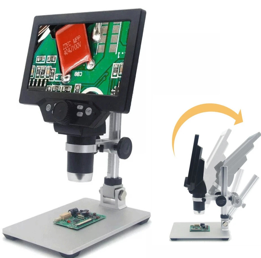
MUSTOOL team has released a new microscope the G1200. This is an upgrade to the G600, addressing several shortcomings like the small screen, the not rotating bracket, and not having a high enough resolution. This time, the new G1200 features a 7-inch HD LCD Screen, the bracket can be rotated at any angle forward and backward to suit your needs, while the lens supports 1-1200x continuous zoom (although this is not the real magnification). These new features will be a good helper for your daily work and soldering. Apart from the features mentioned above, the G1200 also features an HD 12-megapixel sensor, a 7-inch HDLCDy, and a 1-1200 x continuous amplification system. The LCD screen has a good size but we will see that the image quality is not that sharp and you may have some difficulty locating details on it. Also, the screen looks whitish with blacks not looking in contrast. Let’s jump in.
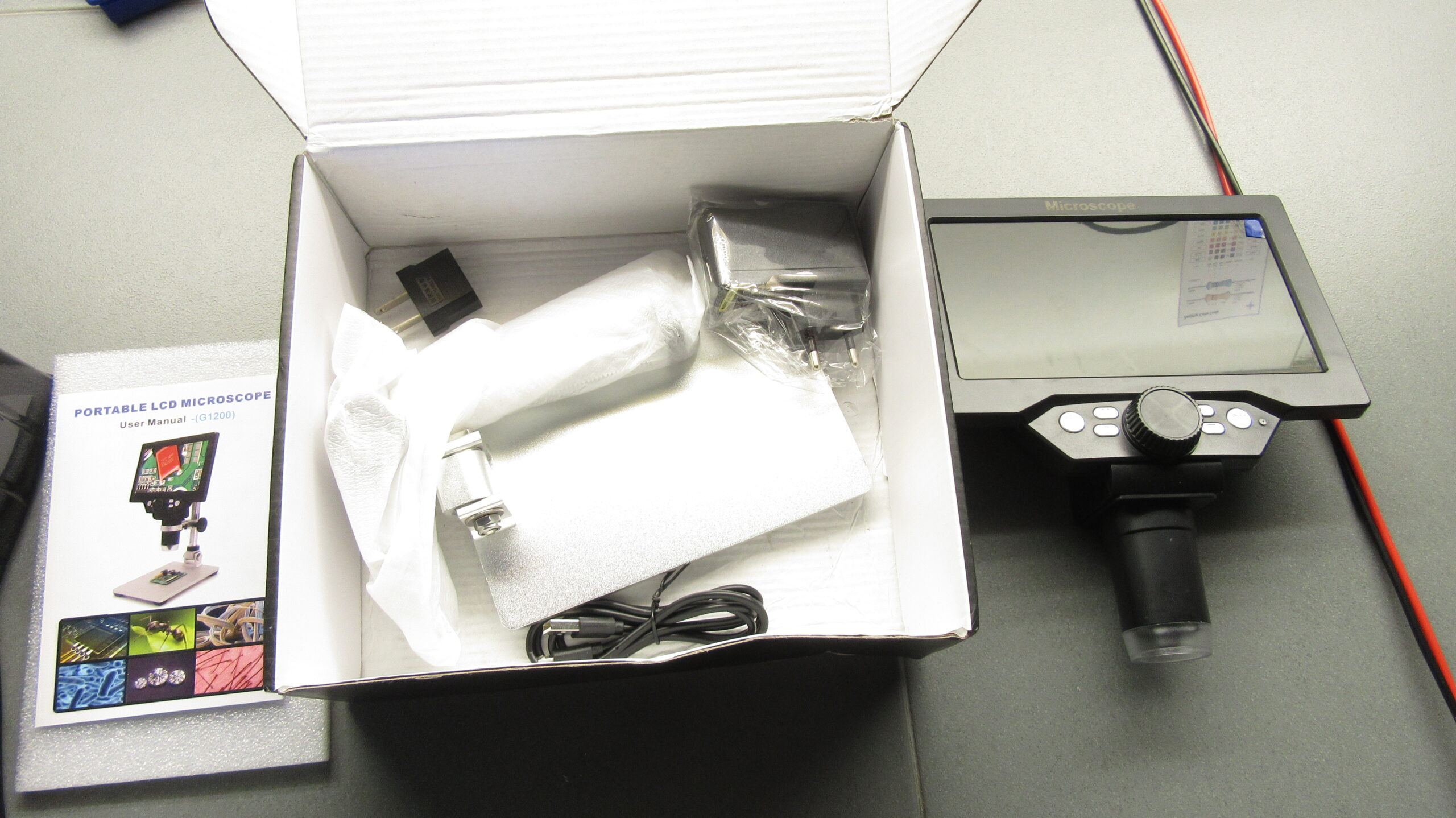
Box Contents

The microscope comes in a carton box and includes:

  • The microscope and LCD assembly
  • A metallic base
  • USB power supply
  • USB cable
  • Socket adaptor
  • Quick StarManualal

The distance between the object is 10mm to infinity (different distances correspond to different magnifications). It also features a built-in ultra-lithium battery, which allows you to work continuously for 4-5 hours (when not in the video recording mode), and sixteen language systems: English, Spanish, Russian, Korean, Japanese, Thai, Hebrew, Portugal, German, French, Italy, Turkey, Czech, Poland, Traditional Chinese, Simplified Chinese.

First Power ON

I mentioned above that the G1200 is an improvement to the G600, let’s see some of the significant improvements:

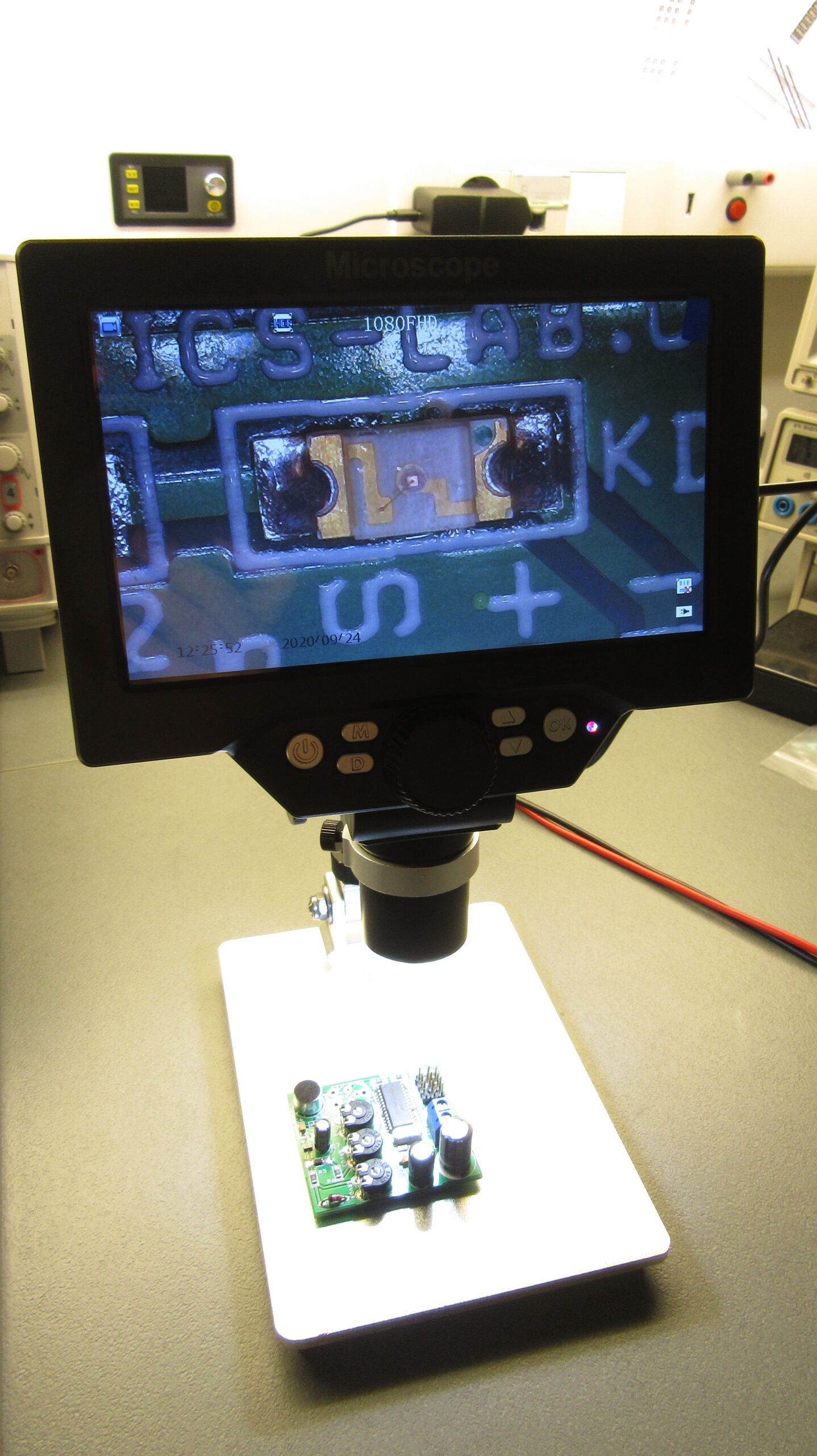
The vertical microscopes (G600) have a serious setback, it is easy to lose sight of the details of the objects due to reflection. Because they are used in many applications such as solder on PCBs, the model designation of some tiny chips and metals requires distinct sight of the details of the objects. However, the G1200 specifically solves this problem because it is an angle-adjustable digital microscope that solves the problem of high reflection. It’s a great experience in the electronics maintenance industry, and it’s important to note that this machine has a larger operable space than the others. It is very convenient to use tweezers, electric soldering iron, and others under this microscope.

Most microscopes are two-gear magnification, either too large or too small. It’s hard to find a suitable view. However, the G1200 is advertised with continuous zoom, and a wide range of viewing options compared to other microscopes, ranging from 1 to 1200 times magnification, although this doesn’t seems real, we noticed that the zoom is almost fixed, and we need to move the microscope closer to the object in the table to get a bigger image. The center knob is only used to focus on the image. These seem improved in comparison to G600 but still luck quality features and a real zoom feature.
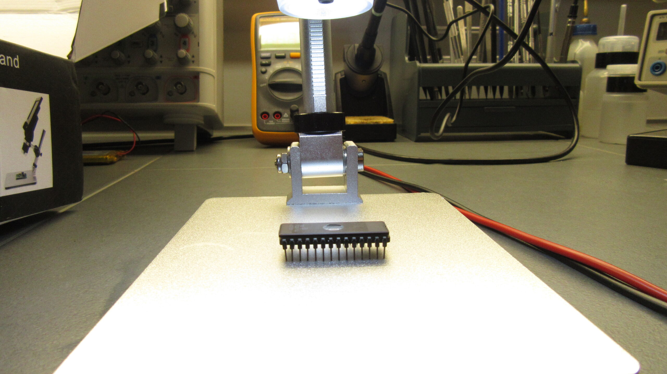
The microscope base

The microscope base looks like it’s from aluminum but I am not sure. The build quality is what to expect for a low-priced microscope and we could also notice a left inclination of the base arm, that was not so straight. You can notice that inclination on the photo below and it seems there is no way to adjust this.

Below we can find the specifications of the G1200. They include:

  • Screen size: 7 inches
  • Screen resolution: 1024X600
  • Screen saver: Off · 30 sec · 1 min · 2 min (optional)
  • Automatic shutdown: Off. 3 minutes. 5 minutes. 10 minutes
  • Hz light source: 50 Hz · 60 Hz
  • Language options: 16 Languages
  • Date adjustment: year, month, day | hour, minute, second
  • Format: YES/NO
  • Default: YES/NO
  • Resolution: 1080FHD, 720P, VGA
  • Circulating camera: Off/3 minutes/5 minutes/10 minutes. When the flash memory card is full, the foremost video data will be deleted and the video will be saved.
  • HDR high dynamic range: On/Off (When power on, the video recording function will be turned on automatically if any object moves under the lens without manual operation.)
  • Exposure compensation: 7 grades for option
  • Date Label: Display/Close-Date and Time can be selected on the screen
  • Photograph delay: Single. 2 seconds. 5 seconds. 10 seconds.
  • Photo pixels: 1.3 M · 2 M · 5 M · 8 M · 10 M and 12 M
  • Continuous shooting: 3 consecutive shots
  • Photo quality: Quality · Standard · Compression
  • Sharpness: Strong · Standard · Soft
  • Color: Nothingness · Black and White · Nostalgia
  • ISO: Automatic · 100 · 200 · 400
  • Exposure compensation: 7 grades for option
  • Photo assist: Anti-hand shock on/off
  • Date label: On/Off
  • Watch: Up,Down,Delete,Protection
  • Mode switching: recording mode / camera mode / playback mode
  • Power supply: DC interface (Micro USB)/ Built-in large 3000mah capacity lithium battery
  • Flash card socket (MicroSD): support 1-128GB. Class10 + speed
  • Light brightness regulator
  • Highlight 8 LED lamps with a continuous service life of up to 100,000 hours

Inspecting some parts

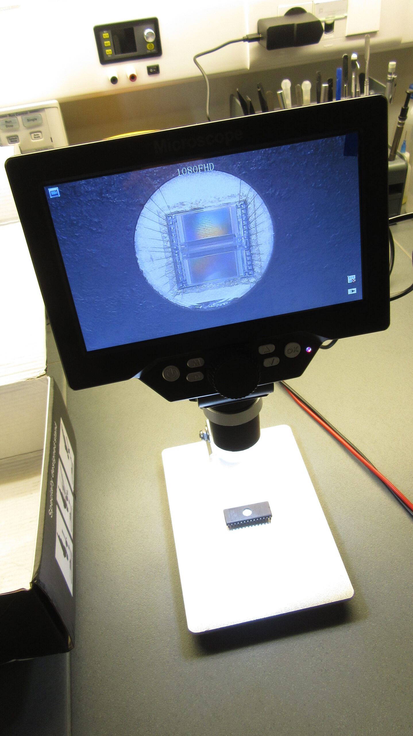
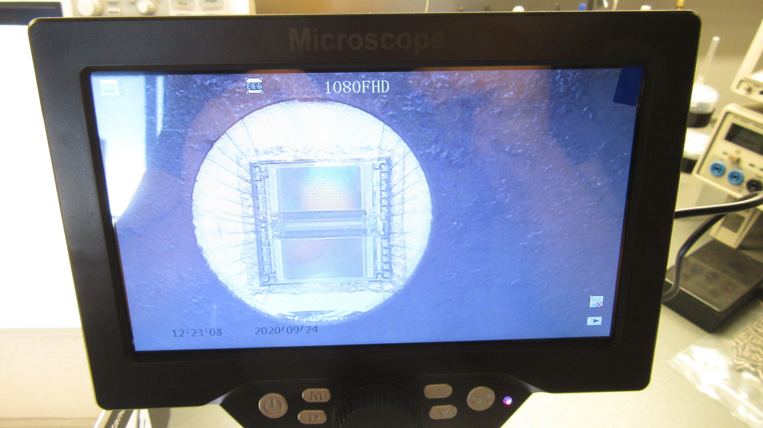
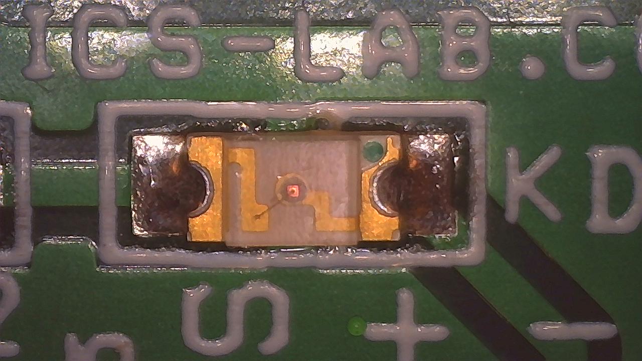
The photo below shows how an SMD LED looks under the microscope. After adjusting the center focus knob, you get the most shard image that is available from the CMOS sensor. In the case of this SMD LED, the focus is good and you can identify small details as there is enough contrast in the scene.

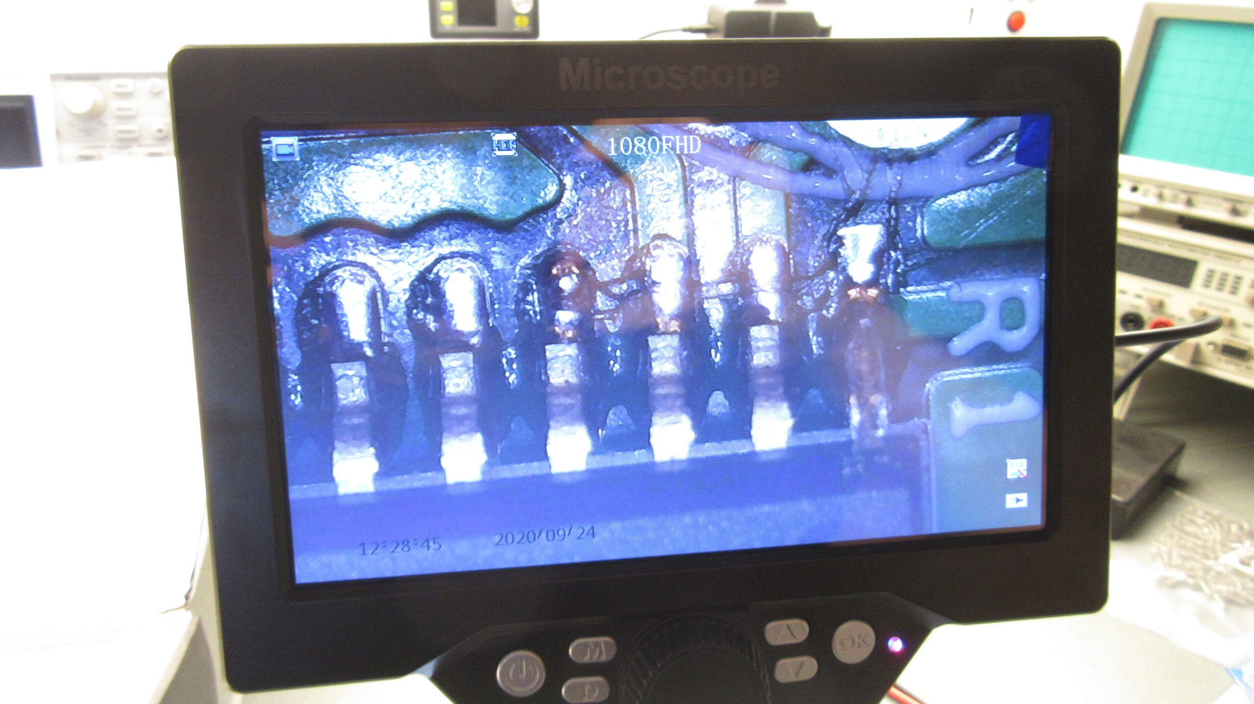
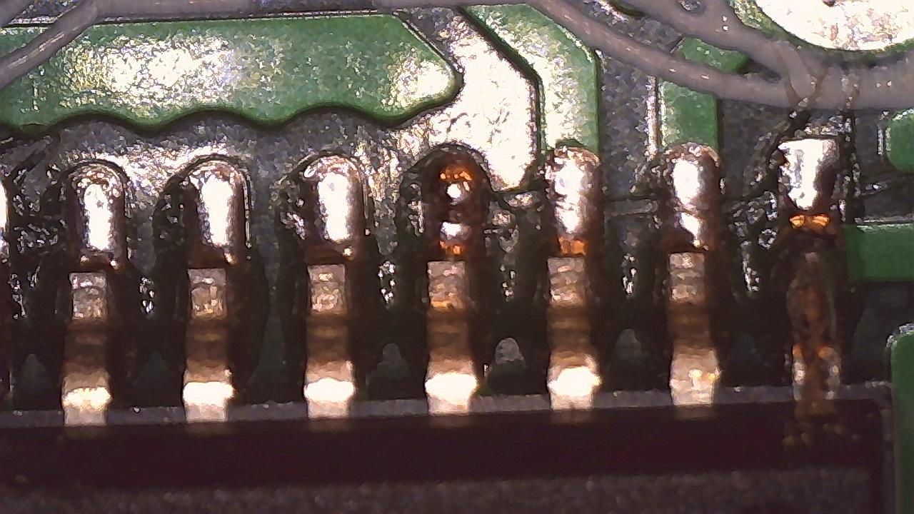
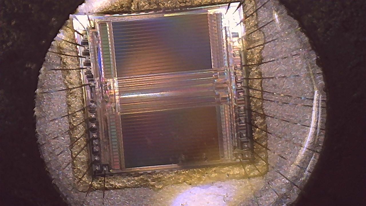
But, when looking at some SMD IC Pins, where the contrast is not very good, you can clearly note that you can’t tell for sure if the pins are soldered or not. In this case, you may have to turn the microscope to another angle to get a better view. This is something that is supported by the available base. Also, it is clearly noted that the LCD contrast is less than enough. We will look just below that the photos captured on the SD card, look much better than the LCD screen.

Sample Photos

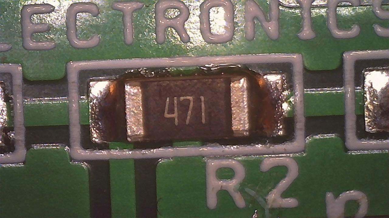
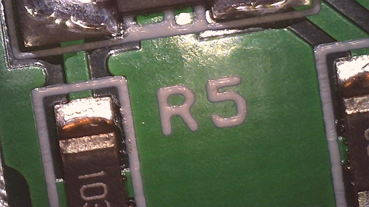
Below you can see some sample captures on the SD card, directly from the microscope. In these photos, you can see the real capabilities of this microscope. It seems the CMOS sensor has some limitations in terms of image quality, but this is something to expect from a low-end instrument. This may not be a serious issue on some applications but may pose a limit on more detailed tasks, where a sharper and clearer image is needed. The maximum image resolution is 1280x720px and it’s as you see below.

Conclusion

The MUSTOOL team has gotten the new G1200 in the right direction but has some distance to cover to gain the prestige of a serious tool. It is indeed correcting the flaws we show with the G600, therefore making it easier to work on your project and help you with SMD soldering and inspecting and it has quite a fair price. The G1200 is available for $68.99 on Banggood.

STMicroelectronics Silicon Carbide Power MOSFETs

STMicroelectronics (SiC) MOSFETs feature very low RDS(on) area for the 1200V rating combined with excellent switching performance, translating into more efficient and compact systems. They have increased switching efficiency and operating frequency with the lowest Eoff vs.

Features

  • Slight variation of switching losses vs. temperature
  • Very high operating temperature capability (200°C)
  • Very fast and robust intrinsic body diode
  • Low capacitance
  • Easy to drive

more information: https://www.st.com/content/st_com/en.html

First Bizen quantum tunnelling transistors launched

A UK startup is to ship its first 1200V power devices using a new silicon architecture called Bizen that fits into TO247 or TO263 packages. by Nick Flaherty @ eenewseurope.com

The first devices to use the Bizen process technology include three parts rated at 1200V/75A, 900V/75A and 650V/32A, available in the industry-standard TO247 or TO263 power MOSFET packages. These are made using standard silicon substrates on conventional, larger-geometry silicon processing lines. The initial pilot line for testing the Bizen technology was set up at Semefab in Scotland.

“To get this level of performance from traditional silicon-based MOSFETs, the device size must be much bigger. 1200V/75A in a TO247 housing can be achieved using wide bandgap materials like silicon carbide, but this approach has other well-known issues,” said David Summerland, CEO and founder of Nottingham-based Search For The Next (SFN) which developed the Bizen technology. This is being used for the parts, called Quantum Junction Transistors (QJT), from subsidiary Wafertrain.

“SiC, for example, takes much longer to process and has a significant manufacturing carbon footprint. Also, regardless of the meilleur casino en ligne roadmaps, SiC does not scale like silicon, and the economic argument that SiC can match silicon does not take into account the advances made possible by Bizen. By contrast, the data we have obtained from physical wafer tests proves that by using Bizen on silicon substrates, our QJTs deliver the same performance as SiC or GaN. Yet the production equipment required to make a QJT is exactly the same as for a standard silicon MOSFET, and the Bizen process adds no extra manufacturing complexity.”

Bizen applies quantum tunelling to a traditional bipolar wafer process. The result is a very rugged and reliable device with the heritage and pedigree of traditional bipolar silicon technology. Bizen also reduces leadtimes from 15 weeks for a CMOS device (although not a SiC MOSFET) to less than two weeks, and halves the number of process layers. The QJTs use these same eight-layer bipolar process.

Wafer tests also show that the Bizen process exhibits an effective current gain of over 1 million, says Summerland. This will enable direct connection between the 1200V/75A QJT power transistor and a low voltage, low current CPU output port such as a PWM for a monolithic design.

“The QJT is the first power device on the Bizen family roadmap. This will shortly lead to the PJT (Processor Junction Transistor), an integrated Bizen device with its own processor which can also be produced on a manufacturing cycle time of eight days, heralding a new era of intelligent power devices,” he said.

SFN has also released other comparative performance metrics for a 1200V/100A part – also in TO247 – which is on its short-term roadmap. The losses at rated current will be a quarter (<300mV) of those exhibited by the SiC device, and its input capacitance will also be four to five times less (< 1pF).

In July Semefab also started making 1200V Schottky diodes on an SiC process and is planning 1700V devices.

more information: www.wafertrain.com/blog

High-end FPGA SOM based on Arria 10 GX FPGA

iWave Systems is introducing a new System on Module (SOM) that is based on Intel’s Arria 10 FPGA GX devices.

iWave Systems, a global leader in the design and manufacture of cutting edge FPGA solutions, is launching a new System on module based on the powerful Intel Arria 10 FPGA GX devices. The Arria 10 FPGA SOM is power-packed with up to 1150K Logic Elements, duel DDR4 RAM with 64 bit and 32-bit storage capabilities. A wealth of high speed I/Os and interfaces that enable the module to fulfil complex data integrity requirements while ensuring faster throughput, reduced latency, and low power execution, accelerating the development of FPGA-based applications in industrial, aerospace, and medical domains.

The SOM is designed to help developers and OEMs with a powerful and well-integrated FPGA platform that help reduce design cycles and accelerate innovations in applications such as “Test and measurement equipment, Control and intelligence equipment, Diagnostic medical imaging equipment, Wireless infrastructure equipment, RADAR, Automation and Military applications.”

Highlights

  • Arria10 FPGA device compatibility
  • GX270, GX320, GX480, GX570, GX660, GX900, GX1150
  • With up to 1150K Logic Elements and 24 High-Speed transceivers
  • 4-GB DDR4 RAM (64bit) from FPGA
  • 24 high-speed transceivers @ 17.4Gbps
  • 48/96 LVDS from BANK 3B & 3C
  • 93 SE from BANK 2A & 3A
  • Dual 240 Pin Board to Board Connector
  • Variable IO voltage support from PMIC
  • Industrial Grade operation

At the heart of the Arria 10 FPGA module from iWave is the Intel Arria 10 GX FPGA, which features 20 nm technology on an F34 package. The module supports seven GX models — GX270, GX320, GX480, GX570, GX660, GX900, and GX1150 which provide varying levels of FPGA logic elements (LEs) ranging from 270K to 1150K, offering a range of options for customers to select the best fit FPGA that serves their applications.

With 500MHz logic core performance, the GX models support 24 transceiver lanes and run on up to 40 percent lower power, which guarantees data integrity and high performance in power and resource-constrained applications. Up to 189 user I/Os and 24 multi-gigabit transceivers each offering a data transfer rate of up to 17.4 Gbit/sec is available on two 240 pin high-speed board to board connectors.

The module can support interfaces like PCIe Gen3 x8, SATA Gigabit Ethernet, USB3.0, etc providing a range of flexible options that help customers towards various use cases. The module’s up to 4 GByte large DDR4 SDRAM facilitates faster throughput and an ultra-low latency data path for real-time executions.

For quick prototyping and time to market, iWave supports a development platform, which includes a powerful configuration of the Arria 10 FPGA SOM with a custom form factor carrier board. Arria10 FPGA Development board supports a wide range of high-speed interfaces like Dual FMC (HPC) Connectors, M.2 SATA, 10G SFP+, 3G/12G SDI In & Out, USB 3.0 TypeC connector and, one PCIe connector to validate Arria10 FPGA high-speed transceivers and other on-board connectors to validate the Arria10 FPGA I/Os. The LPC/HPC FMC connectors provide expansion options on the carrier board, which is compatible with a wide range of plug-in cards such as ADCs, DACs, motor control cards, RF links, etc.

iWave provides full product design engineering and manufacturing services around the Arria 10 FPGA SOMs to help customers quickly develop innovative products and solutions. iWave also offers a comprehensive ecosystem for the Arria 10 FPGA SOM, offering all of the hardware, software, and support materials making it easy to jump-start application development using the Arria 10 GX FPGA.


iWave also provides a development platform that includes a powerful configuration of the Arria 10 FPGA SOM with a custom form factor carrier board. The Arria10 FPGA Development board supports a wide range of high-speed interfaces to validate the Arria10 FPGA high-speed transceivers and other on-board connectors to validate the Arria10 FPGA I/Os.

more information: https://www.iwavesystems.com

New 64-bit i.MX8M Mini Industrial SBC Family from Gateworks

Gateworks is proud to announce a new family of Single Board Computers, the Venice Family. It features a 64-bit NXP™ i.MX8M Mini Quad Core ARM® Cortex™-A53 SoC processor operating at 1.6GHz, LPDDR4 DRAM up to 4GB, and eMMC System Flash up to 64GB.

Compared to the previous Newport family, the Venice family supports multimedia capabilities through a combined MIPI-DSI, MIPI-CSI and I2S Audio header that offers video and audio output and input. Mini-PCIe expansion sockets can be used for 802.11ax/ac/b/g/n WiFi radios, 5G/4G/3G/CATM1 cellular modems and other PCI Express peripherals. Standard peripheral headers support Digital I/O, Analog Input, RS232/RS485/TTL Serial, I2C and SPI. All of the other standard Gateworks features are included, such as the Gateworks System Controller, wide voltage input, PoE support, industrial temperature, optional GPS, optional WiFi/BLE, and open source Linux Software.

As with previous Gateworks SBC families, there will be four standard models: GW7100, GW7200, GW7300, and GW7400. Each model will increasingly grow in size and feature set and is size compatible with previous Gateworks families. The first model to be released is the GW7300 and is available now.

The Venice family will accelerate the time to market on new customer designs in many verticals, including IoT Gateways, Cellular Gateways, Drones and UAVs, Smart Grid & City and Factory Automation.

Venice SBC Family Highlights:

  • NXP™ i.MX8M Mini Quad Core ARM® Cortex™-A53 SoC processor operating at 1.6GHz
  • LPDDR4 DRAM up to 4GB
  • eMMC Flash up to 64GB
  • Multimedia Support via MIPI DSI & CSI and I2S Audio
  • Up to 2x GbE Ethernet Ports with PoE Support
  • Up to 4x Mini-PCIe Sites
  • Optional Ublox ZOE-MQ8 GNSS GPS Receiver with PPS
  • Optional Laird Sterling 802.11b/g/n WiFi & BLE v4.2 Module
  • -40C to +85C Industrial Operating Temperature
  • Linux Ubuntu Board Support Packages
  • Made in the USA
  • Rugged & Industrial design

more information: https://www.gateworks.com/products/imx8-single-board-computers-gateworks-venice/

Microchip Introduces No-Cost, License- and Royalty-Free Ensemble Graphics Toolkit

Graphical user interfaces (GUIs) and interactive touchscreen displays provide intuitive user experiences in applications from robotic and machine controls to medical user interfaces, automotive instrumentation and home and building automation systems. A well-designed GUI enables users to process information more quickly and interact more effectively with a product. Microchip Technology Inc. announced a new GUI development toolkit for its portfolio of 32-bit microprocessors (MPUs) running Linux, helping designers of industrial, medical, consumer and automotive graphical displays to reduce development cost and time-to-market.

Microchip’s new Ensemble Graphics Toolkit is a free and open-source C++ GUI suite for the company’s SAMA5 and SAM9 series of Arm® Cortex®-A5 and ARM926EJ-S processor-based MPUs including the system-in-package and system-on-module products. The Ensemble Graphics Toolkit is optimized for Microchip’s 32-bit MPUs running the Linux operating system. By taking advantage of underlying hardware acceleration, including graphics controllers and video decoders when available, the toolkit provides a high-performance user experience on low and mid-range graphical displays up to XGA (1024 × 768 pixels) resolution.

Optimized code allows a smaller memory footprint, saving BOM cost. The efficient performance relative to other graphics solutions that rely on higher-performance cores and 3D graphical acceleration allows rich GUIs to be created for Microchip’s power-efficient MPUs. In addition, Ensemble Graphics Toolkit and Linux can be optimized for fast cold boot – with boot times of under three seconds from cold reset that is required for applications such as automotive dashboard clusters.

“Whereas other tools require ever higher-performing, higher-power and costlier microprocessors, this no-cost development suite is an enabler that optimizes processing power,” said Rod Drake, vice president of Microchip’s MPU32 business unit. “Developers can achieve modern graphical user interfaces with excellent user experience with a lower bill of material cost, lower power and longevity of solution – while providing a high-end look.”

Microchip’s Ensemble Graphics Toolkit suite is available without licensing or royalty fees to all developers of graphical interfaces. The Ensemble Graphics Toolkit is complementary to Microchip’s bare metal/RTOS-focused MPLAB® Harmony Graphics Suite embedded software development framework that also provides a zero-cost, royalty-free graphical user experience.

The toolkit is fully integrated with Linux4SAM, Microchip’s mainline, Long Term Support (LTS) Linux offering. In addition to supporting Microchip’s MPU families Linux4SAM contains driver support for a broad range of its components including the maXTouch® family of touchscreen controllers, memory devices, power management and analog devices and wired and wireless networking components and modules. Linux4SAM is regularly updated and supports all Microchip MPUs throughout product life.

Development Tools

Microchip’s Ensemble Graphics Toolkit is a complete software and tools framework suite. Training and support are available worldwide at www.microchip.com/EGT.

Pricing

Microchip’s Ensemble Graphics Toolkit is available at no cost and royalty-free for all users and includes full support from Microchip. It is based on the permissive Apache 2.0 open-source license.

Silicon Labs Launches Timing Industry’s Smallest, Lowest Jitter I2C-Programmable Crystal Oscillators

Silicon Labs has introduced a new family of small form-factor, high-performance crystal oscillators (XOs) and voltage-controlled crystal oscillators (VCXOs) for applications that require low jitter and frequency-flexible clock synthesis.

The Si54x/6x Ultra Series XO/VCXOs deliver jitter performance as low as 80 femtoseconds (fs) for integer and fractional frequencies across the entire operating range, providing outstanding jitter margin for demanding applications including data centre interconnect, optical transport, broadcast video and test/measurement. These new products are available with single, dual, quad and I2C-programmable frequency options in an industry-standard 2.5×3.2mm package footprint, making them ideal for space-constrained designs that require a mix of different frequencies.

Ideal for high bandwidth, high-density line cards and small form factor optical modules

Increasing demand for network bandwidth and faster data rates are driving the need for higher speed 400/600/800G optical/Ethernet ports and higher density line cards. With telco and data center applications accelerating 400G deployments, the optical module market is migrating from CFP designs to smaller form factor QSFP-DD, OSFP and CFP2 solutions to help ease the industry transition to higher bandwidth, higher density line cards. These applications require low jitter, highly reliable timing solutions to optimize system bit-error rates and ensure high system availability.

Durable operation in a small footprint

The Si54x/6x are an ideal solution for 400/600/800G coherent optics and 56G/112G SerDes clocking in optical modules and line cards that require high performance in a small footprint. The devices guarantee ±20 ppm operation over a 20-year operating life, making them ideal for long-life cycle applications. All power supply filtering is integrated inside the device, eliminating discrete components that often consume as much PCB footprint as the XO itself. Silicon Labs’ Si54x/6x are drop-in compatible with traditional oscillators while providing <2 week lead times for custom frequencies.

“Data center operators and telco networks are deploying lower-cost, smaller form factor optical modules for line-side and client-side applications, driving the need for space-optimized high-performance timing solutions,” said James Wilson, general manager of timing at Silicon Labs. “Unlike traditional solutions, which may require multiple oscillators to generate all required frequencies, the Si54x/Si56x is a single, unified solution that truly delivers any-rate performance in the industry’s smallest footprint.”
Silicon Labs’ expanding leadership in high-performance timing solutions

These new products further expand Silicon Labs’ industry-leading portfolio of high-performance XO/VCXOs, complementing a broad selection of options spanning general-purpose (800 fs), low-jitter (300 fs) and ultra-low jitter (80 fs) product families in 5x7mm, 3.2x5mm and 2.5×3.2mm package options.

Specifications:

  • Industry-leading jitter performance
  • Wide frequency range with < 1 ppb frequency resolution
  • Single, Dual, Quad, I2C configurations available
  • I2C supports 100 kHz (Standard), 400 kHz (Fast Mode) and 1MHz (Fast Mode Plus) update rates
  • Reduces part numbers: define 4 startup frequencies, use I2C to generate any frequency after startup
  • Excellent supply noise immunity (-80dBc Typ) ensures low jitter operation in electrically noisy systems
  • Excellent temperature and total stability (-40 to +85 °C)
  • 2.5×3.2 mm, 3.2×5 mm, and 5×7 mm footprints
  • 3.3, 2.5, 1.8V supply operation from the same orderable part number
  • Supports all popular formats: LVDS, LVPECL, HCSL, CML, CMOS, and Dual CMOS
  • Superior reliability, 100% electrical testing of every device
  • Samples available with 1-2 week lead times

To help simplify oscillator selection and customization, Silicon Labs offers an array of simple web-based tools:

  • Part number utility enables designers to enter device specifications and generate an orderable part number in minutes
  • Oscillator phase noise look-up tool provides instant access to thousands of phase noise measurements, making it easy to view device phase noise and jitter performance across a wide range of operating frequencies
  • Cross-reference search utility helps customers find Silicon Labs second-source options for high-performance oscillators

Availability

Samples and production quantities of the Si54x/Si56x Ultra Series oscillators are available now.  For device evaluation, Silicon Labs offers the Si5xxUC-EVB universal evaluation board. For more information or to order samples and evaluation boards, visit www.silabs.com/ultra-series.

BOXER-6842: Powering the Next Generation of Edge AI

AAEON, an industry leader in embedded industrial computing, announces the BOXER-6842M, the latest solution in high performance industrial computing. Powered by the 8th and 9th Generation Intel® Core™ processors and supporting graphics cards up to 250W for video capturing applications, the BOXER-6842M is designed for the most intensive applications from Edge AI server to automated optical inspection (AOI).

The BOXER-6842M features the 8th and 9th Generation Intel® Core™ i9/i7/i5/i3 and Xeon® E processors (formerly Coffee Lake/Coffee Lake Refresh), offering top end computing performance. Paired with up to 128 GB of SODIMM memory, the system is designed to deliver the best performance possible to handle processing intensive machine vision and AI applications. Additionally, the BOXER-6842M supports graphics cards up to 250W TDP without the need of a secondary power supply, making setup and deployment even easier.

The BOXER-6842M offers users greater expansion and storage options to better enable edge operation and quick analysis. The system can support up to four 2.5” drives (HDDS or SSDss) and features an M.2 2280 PCIe [x4] slot with support for NVMe, allowing faster read/write speeds and more efficient operating system performance. The system also includes an option of PCI Express configurations, with either one PCIe [x16] with one PCIe [x4] slots, or two PCIe [x8] (in PCIe [x16] form factor slot) with one PCIe [x4] slot. This provides a greater range of support for GPUs, frame grabber cards and AI accelerators such as the AI Core XP8 with Intel® Movidius® Myriad™ X. For applications needing a little bit more power, the BOXER-6842M can support a secondary power supply to power dual graphics cards up to 500W TDP.

The BOXER-6842M is built with several key features to operate in industrial environments. The system features rugged design with wide voltage input (12~24V) and an extensive I/O loadout including six USB3.2 Gen 1 ports, four COM ports, three RJ45 Gigabit LAN ports, and dual HDMI ports; all located on the front of the system to make it easy to manage connections.

AAEON offers industry leading service and support with the BOXER-6842M, from providing technical support to end-to-end solutions to help reduce deployment times and shorten time to market. AAEON also offers manufacturer and OEM/ODM services to help with creating custom configurations, or designing systems from the ground up.

“The BOXER-6842M is built to bring the latest generation of Intel processors to demanding applications including deployment as an Edge AI server,” said Alex Hsueh, Senior Director of AAEON’s System Platform Division. “With AAEON’s industry leading service, our clients can enjoy reliable, high-end performance to power any application they need,” Alex Hsueh added.

Forlinx FETMX8MM-C SoM for Optimized Audio Performance

Forlinx’s SoM FETMX8MM-C contributes to the ever-growing list of tiny, Linux-friendly modules built around NXP’s i.MX8M Mini. This new board focuses on a variety of digital audio processing interfaces. Recent same form factor boards include MYIR’s MYC-C8MMX and Innocomm’s WB15. This new 56 x 36mm SoM FETMX8MM-C module runs Android 9.0 or Linux 4.14 on i.MX8M Mini. It has 2GB DDR4, 8GB eMMC, up to -40 to 75℃ support.

The new SoM FETMX8MM-C centers around the i.MX8M Mini’s specialty at digital audio processing. Other applications with this board may include facial recognition, video intercom, medical, and PDA. This board is powered by Android 9.0 or Linux 4.14 with Qt 5.10.

The SoM FETMX8MM-C is powered by the quad-core Cortex-A53 clocked at 1.8GHz. It also has 400MHz Cortex-M4 MCU and GCNanoUltra (for 3D) and GC320 (for 2D) graphics cores. Forlinx has mentioned that there are H.265 and VP9 decoders that can support 1080P@ 60Hz, which is 50% more efficient but bandwidth and capacity are only 50% of H.264.

SoM FETMX8MM-C and carrier board

The module primarily comes with 2GB DDR4 RAM and 8GB eMMC storage. Media I/O options are 4-lane MIPI-DSI and CSI Audio interfaces include I2S, AC97, TDM, PDM, SPDIF, and 4x SAI, as well as support for FLAC7.1 sound channel output and ring audio input.

The new SoM FETMX8MM-C has support for the Gigabit Ethernet controller and PHY support for 2x USB 2.0. It also includes a standard micro USB connector and USB 2.0 OTG (up to 480 Mbps). Other misc I/O includes PCIe, 2x SD/SDIO, 4x UART, 4x I2C, 4x PWM, 3x eCCPI, FlexSPI, and JTAG.

Overview of FETMX8MM-C System on Module

  • CPU:  NXP iMX8M Mini (@1.8GHz)
  • Architecture : Quad-core Cortex-A53+ single-core Cortex-M4
  • RAM: 2GB DDR4
  • ROM : 8GB eMMC
  • OS: Linux4.14.78+Qt5.10.1, Android9.0
  • Voltage Input: 5V
  • Package: Ultrathin connector(3*80pin, the pitch of 0.5mm)
  • Working Temp Width: 0℃~70℃
  • Dimensions: 56mm×36mm

The SoM FETMX8MM-C is available on Alibaba at a price range of US$65.00 – US$75.00. More information can be found on the Forlinx product page.

DT71 Mini Digital Tweezers

The all-in-one DT71 Mini Digital Tweezers is a measuring tool with full differential input measurement, capable of functioning as an LCR / ESR meter, a digital multimeter, or/and an SMD Tester.

Design with innovation and the highest user experience intentions, the DT71 subvert the appearance restrictions of traditional measuring instruments. It is compact by design and has a unique trinary structure that enables its separation into a digital controller, two testing arms, and two replaceable tweezer tips. Everything about its design is such that it brings comfort and an ease-of-use experience to the working professional. It comes with no physical buttons, but can be operated via a hidden touch button located at the top of the controller, and for long-lasting cordless operations, it comes two powerful lithium batteries (built-in) that promise a 10-hour non-stop operation on a single charge.

It is designed as the perfect bench/handy measuring instrument and can be used to automatically measure different parameters including; resistance, inductance, capacitance, frequency, voltage, and diode, continuity, and so on, giving both the primary and secondary parameters. It utilizes several kinds of replaceable gold-plated tweezer tips to meet various application needs and to enable a higher degree of accuracy in measurements.

Some highlight features of the DT71 Tweezers as detailed on the product page include:

  • Innovative trinary structure that makes it easy to take apart and carry around. It can be separated into the controller, testing arms, and tweezer tips.
  • 90 x 16 OLED display that is rotatable by 360°. Makes it easy to read parameters from any viewing angle.
  • Two magnetic elasticity test arms to help with grasping and easy clipping.
  • The absence of physical buttons but can easily be operated via a hidden touch button at the top of the controller.
  • Ability to automatically recognize left / right-hand operation and adjust the screen display accordingly.
  • Built-in big and dual lithium batteries to provide a longer standby time and balance to the test arms. (One full charge can last for 10 hours non-stop).
  • Ability to automatically measure resistor, inductor, capacitor, voltage, frequency, and diode.
  • Ability to automatically identify components just by grasping them lightly.
  • Ability to provide higher measurement accuracy in various usages, thanks to the variety of gold-plated interchangeable tweezer tips.
  • A built-in micro signal generator that can output multiple signals.
  • Dimensions: 153 mm x 20 mm
  • Weight: 22 grams
  • Charging time: 2 hours

Among other things, the DT71 is perfect for classifying and detecting discrete chip components, as well as debugging and maintaining complex electronic systems. It can be used in the laboratories, workbenches, warehouses, and fields.

More details on the DT71 can be found on the company’s product page, where it currently sells for $59.

TOP PCB Companies