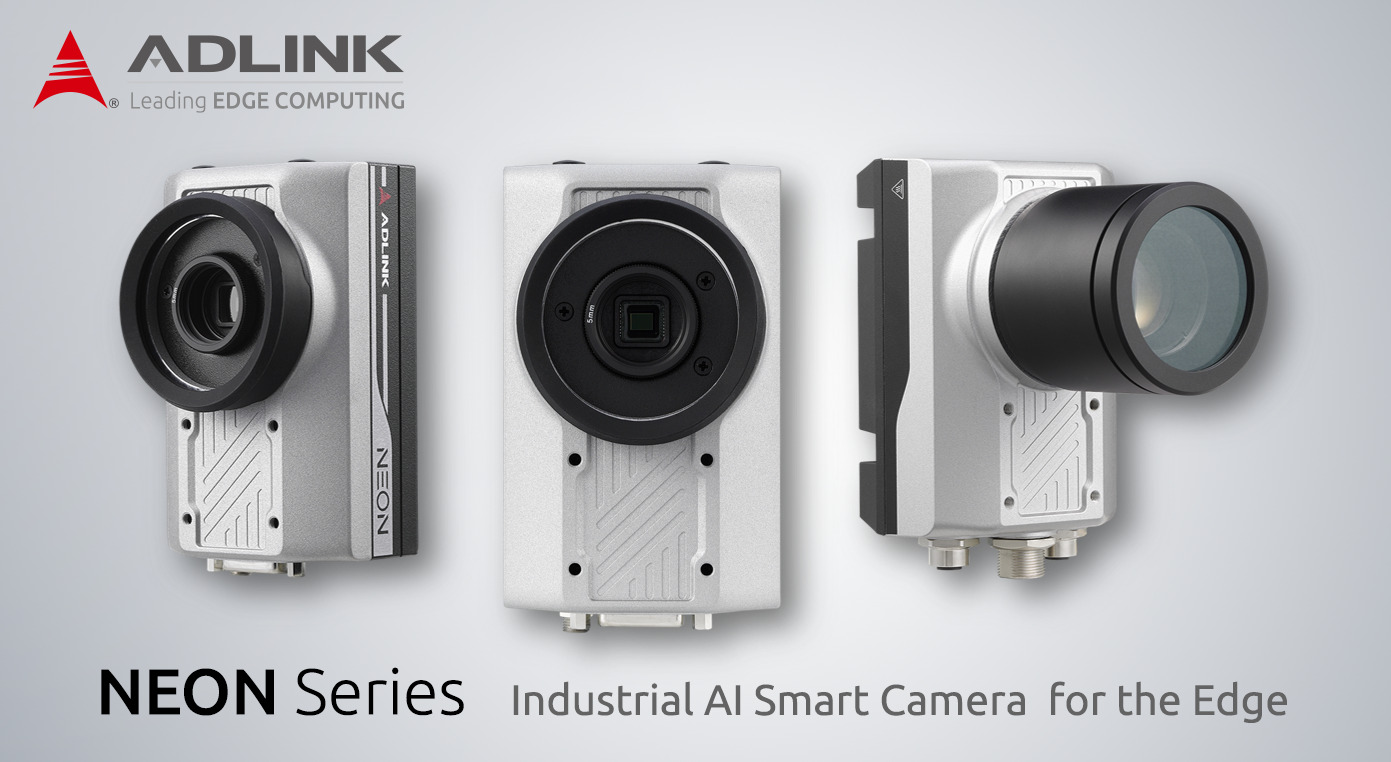
ADLINK’s all new NEON-1000-MDX smart camera and edge vision software come together to quickly add machine vision intelligence and automation within industrial environments
Summary:
ADLINK’s all new NEON-1000-MDX AI Smart Camera combines the Intel® Movidius™ Myriad™ X Vision Processing Unit (VPU) and ADLINK Edge™ software as a turn-key solution for quick and easy machine vision AI deployment
The ADLINK Edge™ software platform now includes Edge Vision Analytics which together, can classify what it sees, become smarter over time, create automation workflows and provide device management for quick proof of concepts
The all new NEON-1000-MDX is now offered as part of the award-winning Smart Pallet turn-key solution proven to deliver a 90% reduction in traditional production time without disrupting current processes
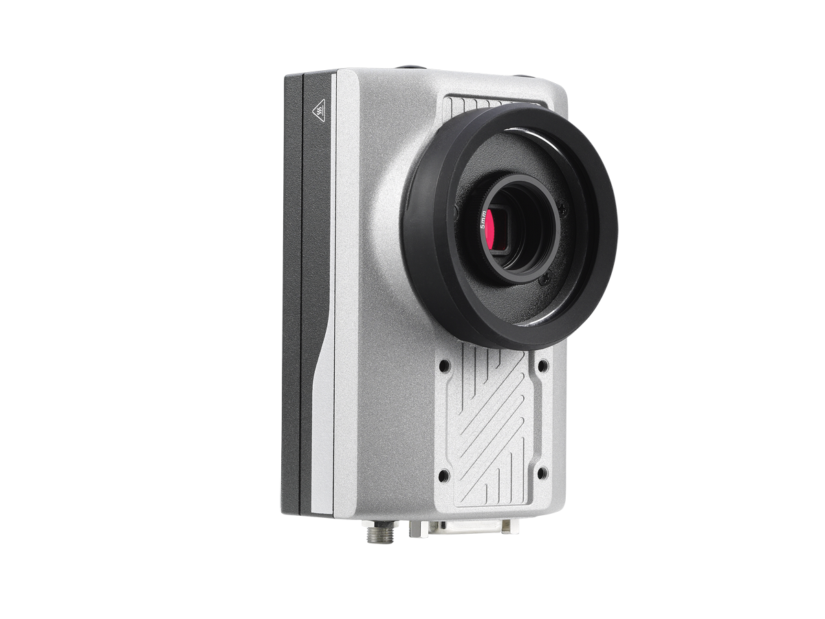
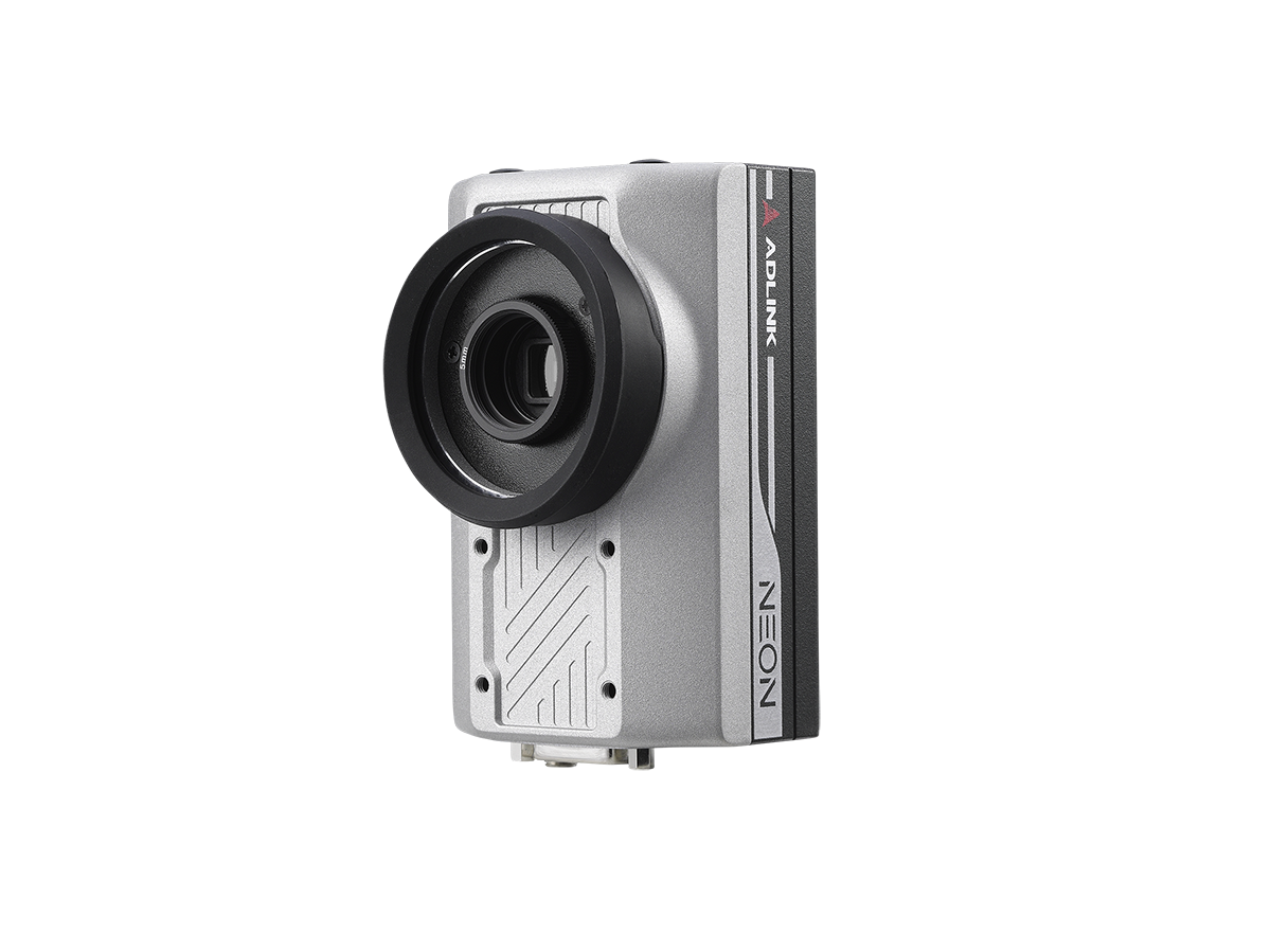
ADLINK Technology Inc., a global leader in edge computing, has launched the all new NEON-1000-MDX Smart Camera series together with its Smart Pallet solution, combining the Intel® Movidius™ Myriad™ X VPU, which supports inference models optimized by OpenVINOTM , and ADLINK’s Edge™ vision software to add AI-based machine vision into existing environments easily and quickly. The all-in-one solution allows machine vision experts and developers to build, test and deploy machine learning (ML) models faster, while giving IoT solution teams and system integrators the tools to connect, stream and automate machine vision work.
“We’re all feeling the pressure of ramped up production during these unprecedented times. Machine vision AI is one of the quickest, easiest and most cost-effective ways to add automation into existing processes without disrupting current workflows,” said Kevin Hsu, Senior Product Manager of ADLINK’s IoT Solutions and Technology Business Unit. “Our Smart Pallet solution, for instance, has proven to deliver a 90% reduction in traditional barcode scanning time while also enabling customized, built-to-order pallets with no changes to the production line other than the smart camera’s installation. Using the highly integrated NEON-1000 effectively decreases the footprint, reliability and compatibility issue and also saves maintenance efforts for customers.”
The Intel Movidius Myriad X VPU (vision processing unit) optimizes ML models and can provide some of the highest AI computing power. Eliminating complex integration of sensor modules, cables and VPU modules, the NEON-1000-MDX Smart Camera simplifies the machine vision deployment process. With the pre-installed EVA (Edge Vision Analytics) SDK, users can deploy neural networks optimized by OpenVINO™ without extra coding or integration efforts using a wide range of ready to use plug-ins based on environment and system requirements.
The new all-in-one NEON-1000-MDX AI smart camera supports product classification and defect detection to maximize production efficiency in smart manufacturing, as seen with the award-winning ADLINK Edge™ Smart Pallet solution. Smart Pallet adds intelligence and automation to manual warehouse fulfillment operations such as receiving, bin picking, packing, shipping and worker safety. Smart Pallet provides an end-to-end integrated system to connect new and existing equipment, capture multiple image data streams and apply the high performance processing power of the NEON-1000-MDX VPUs to enable machine learning and inferencing at the edge.
With the ADLINK Edge™ software platform developers can connect and integrate with any existing cloud, machine learning platform, neural network, industrial camera, machine vision system, piece of machinery and more regardless of vendor. ADLINK’s machine vision AI software can classify what it sees, become smarter over time and also create automation workflows.
“For instance, if a box contains the incorrect order on a conveyor system, it can send an alert to a conveyor’s sorter to divert the box to a re-check area,” said Steve Cammish, VP of ADLINK’s IoT Solutions and Technology. “We’re bringing software developers intuitive programming, automation and device management running on a powerful smart camera designed for AI workloads. The automation here is key- saving time, decreasing costs and reducing complexity.”
ADLINK’s machine vision AI technology has won 5 awards year-to-date. To request a demo, visit ADLINK here.
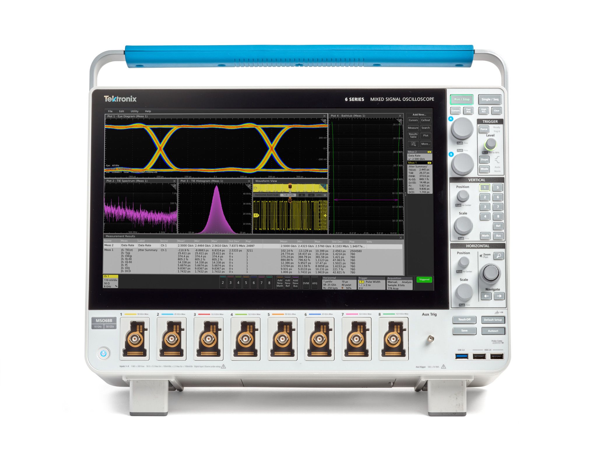
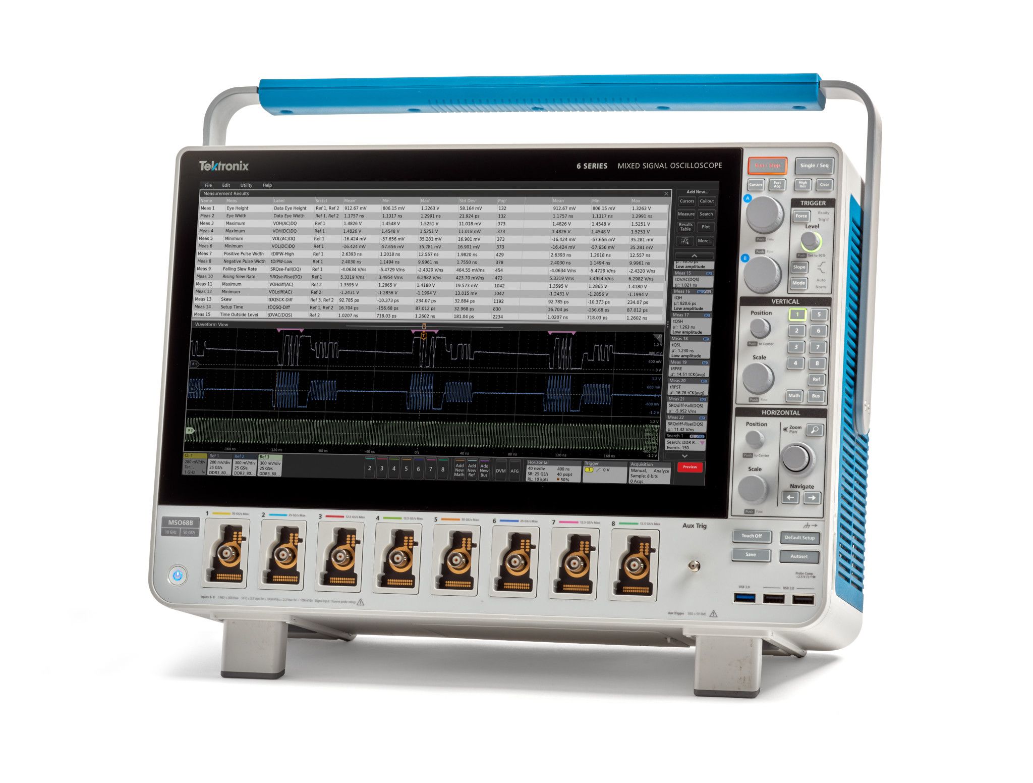
Tektronix, Inc. announced the availability of the new 6 Series B Mixed Signal Oscilloscope (MSO) which extends the performance threshold of the Tektronix Mainstream Oscilloscopes Portfolio to 10 GHz and 50 GS/sec. Developed to meet the demand for high-speed data movement and processing in embedded designs, the enhanced 6 Series B MSO offers leading signal fidelity with12-bit ADCs and extremely low noise, 10 GHz bandwidth and up to 8 FlexChannel™ inputs, enabling users to confidently analyze and debug today’s embedded systems while enjoying exceptional ease of use. Alongside the 6 Series B MSO, Tektronix is also introducing the new TDP7710 TriMode™ Probe, which extends the line of TriMode™ probes to match the advancements of the new oscilloscope.
“At Tektronix, we are dedicated to providing high-performing test and measurement equipment that meets the growing industry need for a precise balance of speed and accuracy,” says Chris Witt, vice president and general manager at Tektronix. “Embedded designs are growing more sophisticated by incorporating additional sensors that generate increasing amounts of data. This instrument addresses the new requirements of testing these systems to advance video, motion and 3D sensing technologies.”
The new 6 Series B MSO goes beyond the expected, allowing top manufacturers to bring cutting-edge and higher performance products to industrial, medical, consumer, and computer markets. Beautifully designed, this instrument is poised for higher-speed embedded designs, demanding mixed-signal design troubleshooting, and accelerating serial bus speeds. The 6 Series B MSO is also highly-effective for diverse applications in semiconductors, power integrity, automotive, defense, aerospace, research, and beyond.
Exceptional Measurement Confidence
The 6 Series B MSO offers a superior combination of bandwidth, sample rate, vertical resolution, low noise and high ENOB, providing exceptional measurements and confidence. With up to 10 GHz of fully-upgradable bandwidth and up to 50 GS/s sample rate, users have better visibility of signals in high-performance designs. This instrument delivers industry-leading signal fidelity, contributing less than 51.1 µV of noise at 1 mV/div and 1 GHz, and less than 1.39mV of noise at 50 mV/div and 10 GHz. The 6 Series B MSO is the industry’s first oscilloscope with bandwidth more than 2 GHz to offer 4, 6 or 8 channels. Each FlexChannel™ input can be converted into 8 digital channels using a TLP058 Logic Probe for added visibility.
Premier Analysis
The 6 Series B MSO offers a range of options to streamline protocol decoding, compliance testing for serial standards, jitter analysis, and power analysis. Built-in digital down converters (DDCs) behind every channel enable multi-channel spectrum analysis, and spectrum measurements are synchronized with time domain waveforms to enable correlation between RF and time events.
Outstanding User Experience
The 6 Series B MSO’s responsive 15.6 inch HD capacitive pinch-zoom-swipe touch display is the industry’s largest, providing an intuitive drag and drop, object-oriented user interface. This series expansion includes the world’s first 10 GHz oscilloscope that is capable of switching between Windows 10 and closed operating systems, without loss of performance or ease-of-use. The 6 Series B MSO contains a removable SSD; which, along with optional security licenses, enables use of the oscilloscope in secure environments by minimizing cybersecurity threats. The TekVPI™ probe interface, known for versatility and ease-of-use, communicates seamlessly with a wide range of probes, to simplify setup and reduce errors, furthering an outstanding user experience for engineers. The new TDP7710 TriMode Probe is a perfect example, with 10 GHz bandwidth and the ability to switch from making differential to common mode to single-ended measurements, without having to reconnect the probe.
Even in a digital world, classic analog clocks have a timeless style. This simple but universal technology is presented in the article. The implemented project uses a dual-rail GreenPAK™ SLG46121 which can perform all the active electronic functions needed in an analog clock, including motor driver and crystal oscillator. Additionally, GreenPAK ICs are low-cost and tiny devices that fit right in with smartwatches. As an easy-to-build demonstration, the author obtained a cheap wall clock, removed the existing board, and replaced all the active electronics with one GreenPAK device.
Background: Lavet Type Stepper Motors
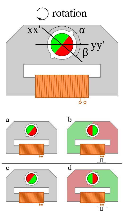
A typical analog clock uses a Lavet type stepper motor to turn the pinion gear of the clock mechanism. It is a single-phase motor that consists of a flat stator (stationary part of the motor) with an inductive coil wrapped around an arm. Between the arms of the stator lies the rotor (moving part of the motor) which consists of a circular permanent magnet with a pinion gear attached to the top of it. The pinion gear coupled with other gears moves the clock hands. The motor works by alternating the polarity of the current in the stator coil with a pause between the polarity changes. During current pulses, the induced magnetism pulls the motor to align the poles of the rotor and stator. While the current is off, the motor is pulled to one of two other positions by reluctant force. These reluctance rest positions are engineered by the design of non-uniformities (notches) in the metal motor housing so that the motor rotates in one direction (see Figure 1).
Figure 1: Lavet Type Stepper Motor Rotation Pattern (Source: en.wikipedia.org, accessed in 2018)
Motor Driver
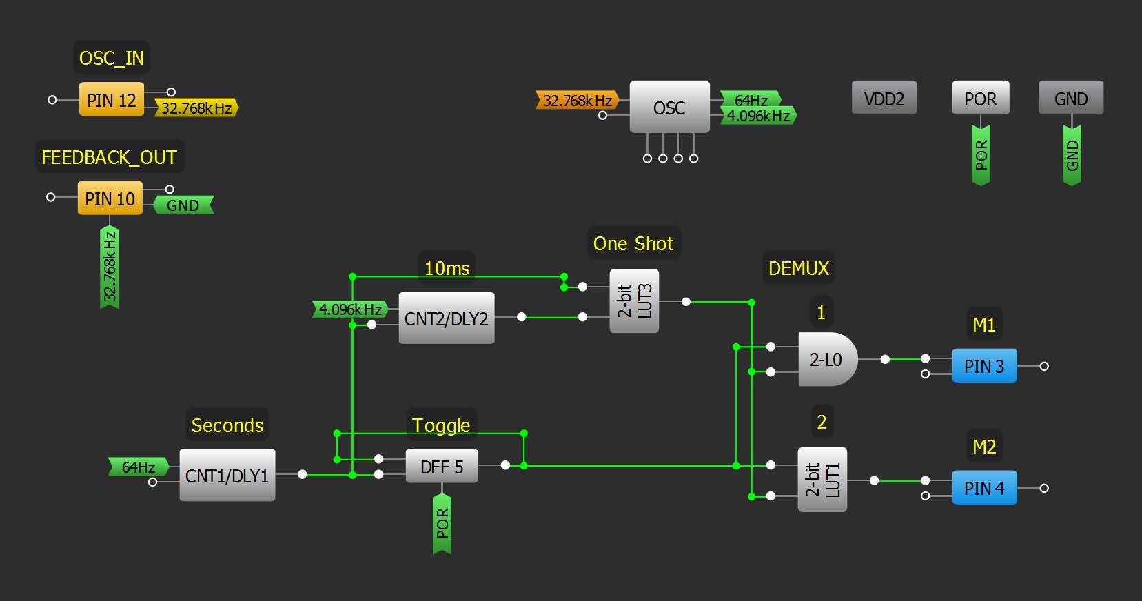
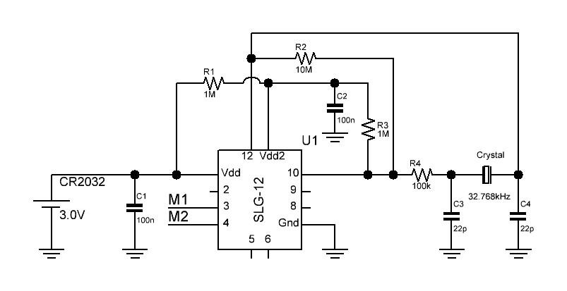
The attached design uses an SLG46121V to produce the required current waveforms through the stator coil. Separate 2x push-pull outputs on the IC (labeled M1 and M2) connect to each end of the coil and drive the alternating pulses. It is necessary to use push-pull outputs for this device to operate correctly.
The waveform consists of a 10 ms pulse each second, alternating between M1 and M2 with each pulse. The pulses are created with just a few blocks driven from a simple 32.768 kHz crystal oscillator circuit. The OSC block conveniently has built-in dividers to help divide down the 32.768 kHz clock. CNT1 outputs a clock pulse every second. This pulse triggers a 10 ms one-shot circuit. Two LUTs (labeled 1 and 2) demultiplex the 10 ms pulse to the output pins. Pulses are passed to M1 when DFF5 output is high, M2 when low.
Figure 2: Circuit Diagram of Internal Connections
Crystal Oscillator
The 32.768 kHz crystal oscillator uses just two pin blocks on the chip. PIN12 (OSC_IN) is set as a low-voltage digital input (LVDI), which has a relatively low switching current. The signal from PIN12 feeds into the OE of PIN10 (FEEDBACK_OUT). PIN10 is configured as a 3-state output with input wired to the ground, making it act like an open drain NMOS output. This signal path naturally inverts, so no other block is needed. Externally, the PIN 10 output is pulled up to VDD2 (PIN11) by a 1MΩ resistor (R4). Both PIN10 and PIN12 are powered by the VDD2 rail, which in-turn is current limited 1 MΩ resistor to VDD. R1 is a feedback resistor to bias the inverting circuit, and R2 limits the output drive. Adding the crystal and capacitors completes the Pierce oscillator circuit as shown in Figure 3.
Figure 3: Circuit Diagram of External Connections
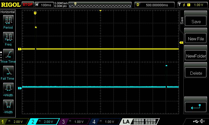
Results
VDD was powered by a CR2032 lithium coin battery which typically provides 3.0 V (3.3 V when fresh). The output waveform consists of alternating 10 ms pulses as shown below in Figure 4. Averaged over a minute, the measured current draw was roughly 97 uA including the motor drive. Without the motor, the current draw was 2.25 μA.
Figure 4: Motor Driver Output Waveform, 10 ms on, 990 ms off
Conclusion
This article demonstrates the usage of a GreenPAK IC aimed to create a complete solution for driving an analog clock stepper motor. This example can be the basis for other more specialized solutions. This solution only uses a portion of the GreenPAK IC resources, which leaves the circuit open to additional functions limited only to the designer imagination.
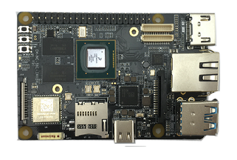
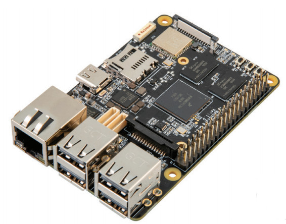
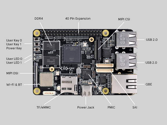
Avnet’s NXP i.MX 8M Mini SBC seems very familiar if you ever seen a Raspberry Pi, as their I/O looks rather similar at first glance, but is it more than that? Actually, yes.
MaaXBoard Mini is a single board computer based on the NXP IMX8M Mini SOC series, designed by Avnet Manufacturing services. From the outside, it comes at a compact size with some interesting peripheral interface options, such as Gigabit Ethernet, USB 2.0 host, MiPi-DSI, MIPI-CSI, Micro SD card, Wi-Fi, Bluteooth and GPIO. Regarding the hardware, it’s based on the NXP’s first embedded multicore applications processor, which is built using the advanced 14LPC FinFET process technology, a 14 nanometer fabrication process, providing more speed and improved power efficiency over its predecessor, the i.MX 8M. However, it comes with a more limited feature set than the earlier-released MaaXBoard, where the MIPI-DSI is preffered over HDMI, leaving you with a smaller resolution of 1080p at 60fps instead of the 4K 60fps, paired with a different GPU, the 4GB DDR4 is downgraded for a mere 2GB, are some of the most noticeable changes.
The full list of specs are:
CPU Multicore Processing:
4x Cortex-A53 core up to 1.8GHz per core (32KB L1-I Cache / 32 kB L1-D Cache / 512 kB L2 Cache)
1x Cortex-M4 core up to 400MHz (16 kB L1-I Cache / 16 kB L2-D Cache)
Wi-Fi + Bluetooth 4.2
As interfaces are concerned, the name Mini is surely not applied
As software is concerned, you can be assured of Android 9.0 and Linux (Yocto and Debian) support, containing an interesting amount of documentation to work with each of them.
Regarding the accessories, you are not limited, as you can get components such as a compatible 7” display for $51.02, a MIPI-DSI camera module for an extra $12.24, a FT232 USB to UART module for $5.92 and a USB to CAN module for $28.57.
Some of the possible applications for this SBC are family entertainment systems, HMI interfaces, computer vision, and other AI and imaging projects. It comes at a cost of $72.50.
What do you think of this board? Is it just a lookalike of the Raspberry Pi for you? My opinion is that it’s quite a bit more than that, justifying the higher price tag with faster hardware and more interface options.
If you ever made a PCB, you quickly realized that the component library of the PCB design software is usually pretty limited for such sophisticated programs. Usually, one has to resort to external tools to access the schematic symbols, footprints and 3D models, or design our own in the designer, which takes some precious time and is arguably the least enjoyable step of the process. Autodesk released Library.io to help you in that process.
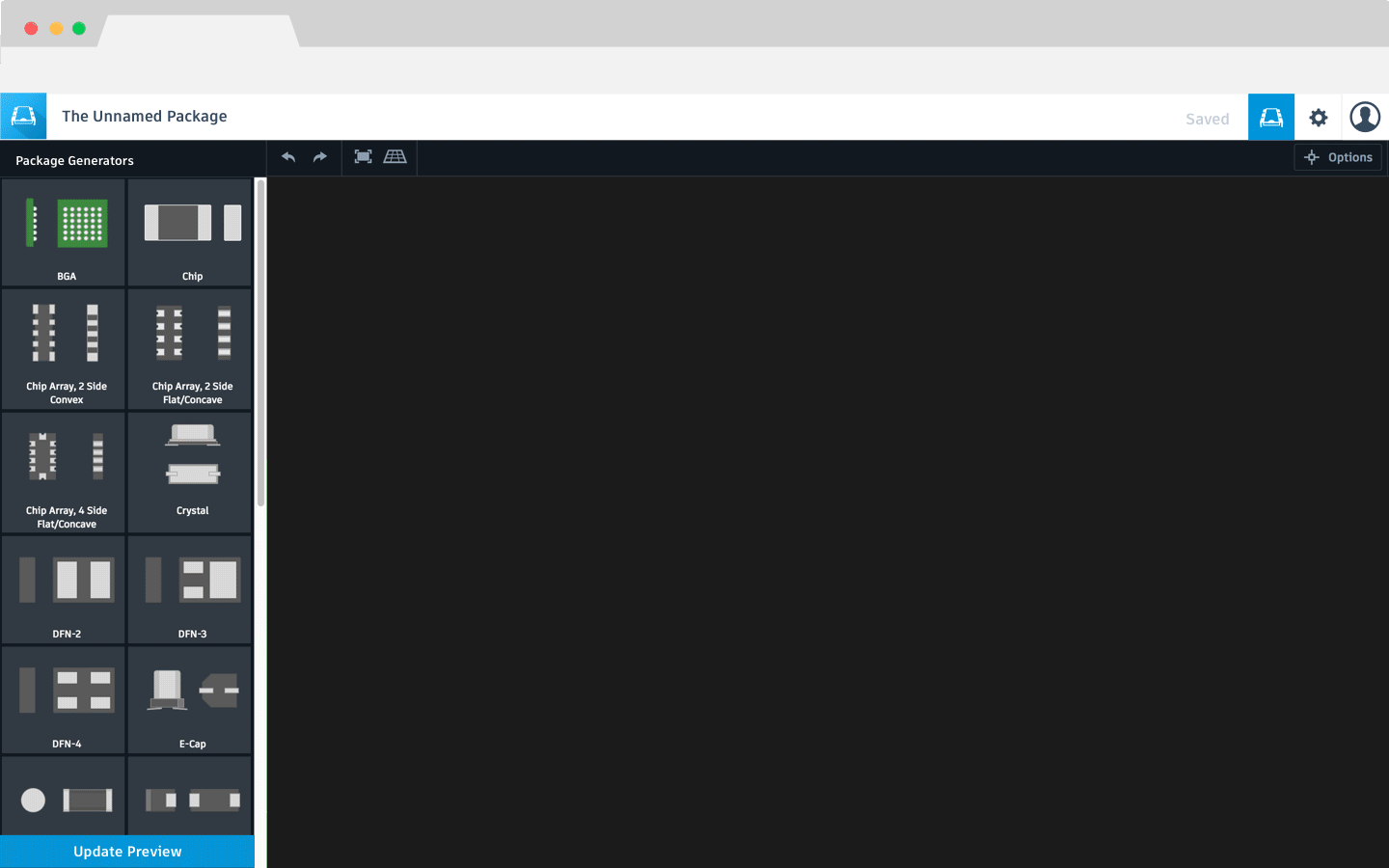
The idea behind Library.io is to simplify this process, by helping you generate PCB packages by entering a few dimensions from the datasheet of the desired component on the browser, from which you can export to your favorite software. Simple, right? Actually, it is! Library.io creates manufacturing-ready PCB packages, where the geometries are generated to meet IPC-7351B standards.
Autodesk’s Library.io in action
I decided to give it a try: after clicking on “Create a new package”, you are greeted with a package generator selector menu, containing a wide range of packages as a starting point (such as BGA, crystal, DIP, QFN, SOT23, among others) on the left, and a package inspector on the right, where you can observe a high-quality 3D rendering of your model, allowing you to move the camera to better inspect the package, glance at the footprint and the model. By selecting one of the available packages, you enter a detailed view, where the package’s measurements are shown, similarly to what you find in the mechanical section of the datasheet. There, you insert all the mechanical measures, choose the number of pads and their shape, along with the density level of the package, configure the silkscreen, and the tolerances for fabrication and placement. Finally, to export, you just hit finish and export it to your favorite CAD software, which may or may not be an easy process, depending on the software you are using, as Autodesk owns Eagle and they probably want you to use it.
Besides the ability to design your own package from scratch, the website also allows you to browse an extensive library of components, which might be a good idea to check before looking up the datasheet for the dimensions, saving you from the already small amount of work.
There are also some extra functionalities, some of which require a premium subscription: you can import and store component libraries on the cloud, create managed folders, that can be shared with an entire team, allowing you to share your component library with your coworkers.
To wrap this up: Autodesk delivers with Library.io an interesting tool that can help speed up the development of your future PCB’s. Do you intend to use it in your future projects?
Artila Electronics, which specializes in the development and manufacture of Linux-ready Arm embedded industrial computers, is glad to announce SBC-7530, an ARM based Cortex-A7 turnkey single board computer, delivers stable, strong system performance in a low power platform; it’s designed specifically for applications which require multiple I/O connection, networking connectivity and high performance graphic interfaces. With arm processor coupled and the open Linux operating system provides the backbone for innovative smart IoT solutions.
Artila brings SBC-7530 as ready solution for industrial HMI, an ideal single board computer based on Arm cortex-A7 for different automation and display applications. The use of our turnkey single board computer systems minimizes development risks for reliable, rugged design with arm processor also it’s compact size allow to be embedded in devices where space is very limited. The computers are also very efficient, giving them an edge where saving on power is concerned. Artila’s SBC-7530 is self-contained that generally less capacity than a multi-board computer. It makes a cost effective solutions for industry and, because they are it is relatively easy to swap one out for the other if a computer needs to be replaced.
To fulfill all requirements for industrial applications, it supports one miniPCIe slot that easily deploy connectivity technology / RF modules to achieve wireless network communication and position. Such as LTE/4G, Lora both wired / wireless LAN. It is also equipped 4 x UART ports with RS-232/485 support, 1 x CAN bus 2.0, 2 x OTG/HOST USB , 1 x SD card slot. SBC-7530 demonstrates it is not only the best hardware solution for industrial markets, but also flexible enough to be applied to various applications such as automation control, human-machine interfaces, industry controllers, and IoT device related applications.
With its high performance and rich I/O interface appeal, SBC-7530 is extremely power saving, with low power consumption and the reliable power circuit design, users can confidently develop the most solid, stable and durable industrial applications.
For more information regarding SBC-7530 or other Artila products, please visit www.artila.com, or email to sales@artila.com.
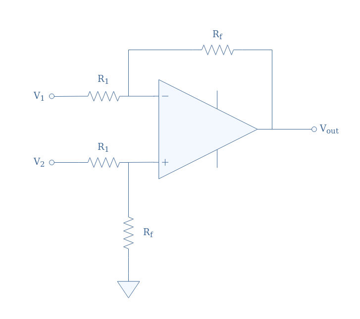
In the previous tutorials, we talked about the inverting op-amp and non-inverting op-amp, we considered configurations that take a single input on either pin “-” or “+” of the operational amplifier, while the other pin is grounded.
However, it is possible, as we will see during this article, to supply both inputs of an op-amp with signals in order to obtain an output that is directly proportional to the input difference. This new configuration is commonly known as a differential amplifier.
We introduce this new configuration in the first section where we present its functioning and demonstrate its output expression.
A simple example of a differential amplifier along with some basic differential-based applications is presented in the second section.
Finally, the last section briefly presents the instrumentation amplifiers which are essential differential-based configurations found in acquisition chains to treat sensor outputs.
Presentation
The goal of this section is to introduce the reader to the differential amplifier configuration and to demonstrate its output expression.
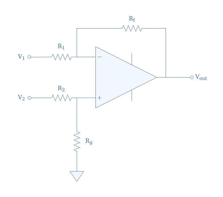
In Figure 1, we present the circuit representation of the basic differential amplifier. The inputs are labeled V1 and V2 and are in connection with the op-amp inverting and non-inverting pins through the resistors R1 and R2. The output is labeled Vout and the resistors Rf and Rg stand respectively for “feedback” and “ground”.
fig 1: General differential amplifier op-amp circuit
In the following, we will suppose the op-amp to be ideal, which is a very good approximation of modern real amplifiers. As a consequence, we have no currents entering through the pins – and + of the op-amp, moreover, the equality V+=V– between the potentials at the same pins is satisfied.
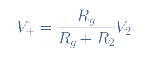
The voltage V+ is determined by the voltage divider formula linking R2 and Rg:
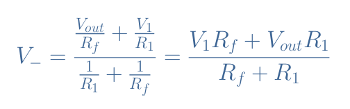
The voltage V– can be written thanks to Millman’s theorem which stipulates that the potential at a node can be written as the sum of the currents entering the node and divided by the sum of the admittances in each branch:
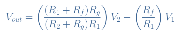
Since we suppose V+=V–, both previous equations are also equal. After rearranging this equality, we finally obtain the output expression for a differential amplifier in the general case, which is a superposition of both inputs V1 and V2:
eq 1: Differential amplifier output expression in the general case
Differential mode
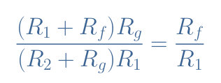
The configuration R1≠R2≠Rf≠Rg is however never used in real circuits. What we should aim for when designing a differential amplifier is to get an output of the form Vout=A(V2-V1), with A being a common factor.
In the following paragraphs, we show under which condition (that we call differential condition) this common factor can be written.
In order to get a common factor for V1 and V2, the following equality must be satisfied:
After some basic simplification steps, the differential condition can finally be written Rf/R1=Rg/R2. In this case, we obtain indeed Vout=A(V2-V1) with A=Rf/R1.
We can even simplify the circuit by choosing R1=R2 and Rf=Rg (which still satisfies the differential condition and with again A=Rf/R1):
fig 2: Differential amplifier operating in differential mode
Subtractor mode
If we add the conditions R1=Rf and R2=Rg, not only we satisfy the condition to write the output under the form Vout=A(V2-V1) but also we get A=1.
In this case, we cannot talk of the circuit as a differential amplifier since the difference V2-V1 is not amplified, we instead label the configuration as a subtractor with Vout being directly equal to the input difference.
Differential amplifier examples
As stated in the introduction, differential amplifier op-amps can be very useful to process the output signal of a sensor. We first present some very simple sensors that are resistors which resistance value depends on an external physical parameter.
In the second part, we need to present what is a Wheatstone bridge before focusing on the third part which deals with the integration of these sensors in a differential amplifier circuit to understand how the signal is processed.
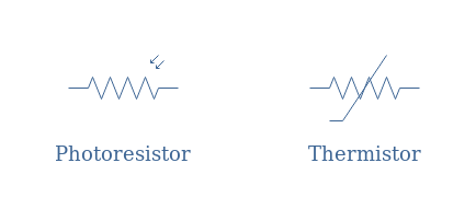
Dependent resistor
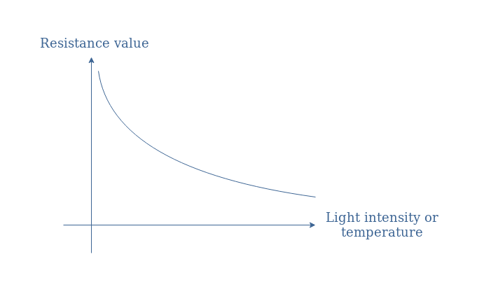
In the following, we present the basics of resistors which resistance values depend on the light intensity (photoresistor) or on the temperature (thermistor).
fig 3: Photoresistor and thermistor symbols
A good modelization for both photoresistor and thermistor resistance values is to consider an exponential decrease with an increase of the light intensity or temperature:
fig 4: Transfer function of dependent resistors
Wheatstone bridge
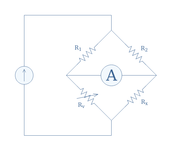
A Wheatstone bridge is a measuring circuit composed of 4 resistors interconnected in a loop configuration such as shown in Figure 5. One of the resistors has an unknown value (Rx), one is a variable resistor (Rv), and two have known and fixed values (R1 and R2).
fig 5: Circuit representation of a Wheatstone bridge
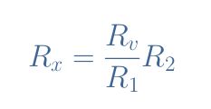
We won’t explain here the details about the measuring procedure of a Wheatstone bridge but we will assume that when no current is detected by the galvanometer (or amp meter) across the nodes R1-Rv and R2-Rx after adjusting the value of Rv, the resistance Rx is given by Equation 1.
This condition is also known as the balancing condition of the Wheatstone bridge.
eq 1: Unknown resistance value of a Wheatstone bridge
Light/temperature detection
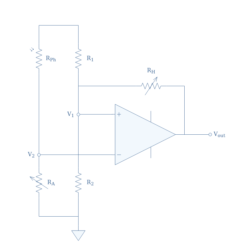
In the following Figure 6, we present a light-detection circuit based on a differential amplifier configuration, including a Wheatstone bridge with resistors R1, R2, the photosensitive resistor RPh which plays the role of the unknown resistor, and a light-adjusting resistor RA which plays the role of variable resistor. The feedback resistor RH adjusts the hysteresis.
Note that a temperature-detection circuit consists only of replacing the photoresistor by a thermistor.
fig 6: Light-detection circuit
The goal of the resistance RA is used to set the “reference” light-level, indeed, when a certain level of light changes the value of RPh, we can adjust RA in order to balance the Wheatstone bridge and get a zero differential input V2-V1, and therefore no output signal as well.
When the light intensity changes, the circuit becomes unbalanced and a voltage difference V2-V1 appears. Even with a small luminosity change, the op-amp will amplify the differential signal in order to correctly detect it and eventually process it in the next stages of the circuit.
One possible way to process the signal is by connecting a LED to the output of the op-amp. The LED is only ON when the output voltage is above a certain value, it stays OFF otherwise. For the configuration presented in Figure 6, the LED would turn ON in the absence of light making it a “darkness detector”. To get the opposite effect and build a “light detector”, we simply need to exchange the positions of RPh and RA.
Instrumentation amplifiers
One of the limitations of differentials amplifiers when it comes to process sensors outputs is its relatively low input impedance. Indeed, the input impedance of the general configuration presented in Figure 1 is equal to R1+R2, which is much lower than the input impedance of a common non-inverting op-amp.
In practice, for this reason, differential amplifiers are never used alone for processing sensor outputs as their low input impedance can bias what the source (sensor in our case) provides (see the tutorial op-amp building blocks for more information).
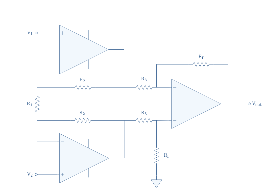
The solution to increasing the input impedance is to connect voltage followers before the inverting and non-inverting inputs of the differential amplifier. This configuration, known as an instrumentation amplifier, is presented in Figure 7 below:
The voltage drop across the resistor R1, which is the input of the differential amplifier, is equal to V2-V1, except that this time, the sources of the signals V1 and V2 sees a very high input impedance thanks to both buffers.
Conclusion
The primary goal of a differential amplifier is to amplify a voltage difference, that corresponds to the difference between the two input signals applied at its inverting and non-inverting inputs.
We have seen that in the general case (with arbitrary resistors), the op-amp doesn’t really amplify the difference since a difference factor is found for V1 and V2. It is actually more interesting to equalize the input resistances and the feedback and ground resistances (which we called the differential condition) in order to get an output of the form Vout=A(V2-V1).
In the second section, we dealt with a light/temperature detector circuit based on a differential amplifier. First, we briefly presented how a photoresistor/thermistor and Wheatstone bridge worked. The circuit shown in Figure 6 merges these different circuits and elements in order to create a simple light/temperature sensor.
However, the low input impedance that this circuit presents is its bigger disadvantage. In order to solve this problem, buffers are usually placed as an input to the differential amplifier as we present in the last section about instrumentation amplifiers.
MPS’ quad-output, DC/DC stepdown power module features up to 2 A and 3 A per output
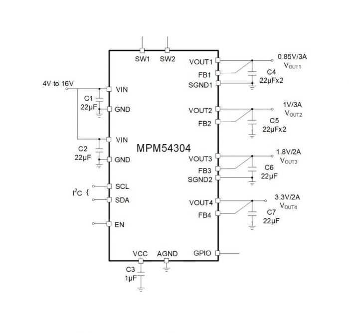
Monolithic Power Systems’ MPM54304 is a complete power management module that integrates four high-efficiency step-down DC/DC converters, inductors, and a flexible logic interface. This COT control DC/DC converter provides a fast transient response. Its default 1.5 MHz switching frequency greatly reduces the external capacitor size. The output voltage is adjustable through the I2C bus or preset by the three-time programmable MTP (multiple-time programmable) e-fuse. The power-on/off sequence is also programmable via the MTP. Full protection features include UVLO, OCP, and thermal shutdown. The MPM54304 requires a minimal number of external components and is available in a space-saving LGA (7 mm x 7 mm x 2 mm) package.
Specifications
Configurable, multi-functional GPIO pin
I2C and configurable parameters:
Paralleling channel 1 and 2
Paralleling channel 3 and 4
Switching frequency
Output voltage
Overcurrent and overvoltage protection threshold
Power-on and power-off sequencing
Forced PWM or auto-PWM/PFM
4 V to 16 V operating input range
Wide output voltage:
I2C programmable: 0.55 V to 5.4 V
External resistor divider: 0.6 V to 7 V or VIN x DMAX if VIN <7 V
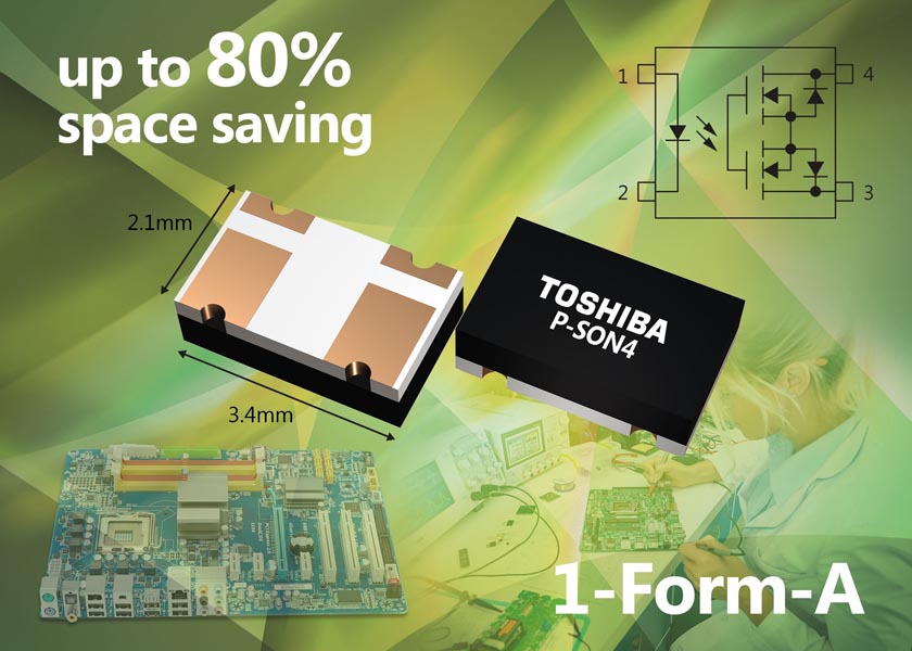
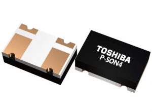
Toshiba Electronics Europe continues to drive innovation forward in optoelectronics with the addition of more photorelays to its expansive portfolio. All three of these devices are housed in the new P-SON4 package format. They are able to deliver very strong performance characteristics while taking up significantly less board space than commonly used SOP packages.
The TLP3480, TLP3481 and TLP3482 each have OFF-state output terminal voltage ratings and ON-state current ratings that are comparable to larger SOP-packaged devices – with these parameters ranging from 30 V and 4.5 A (for the TLP3480), 60 V and 3 A (TLP3481) to 100 V and 2 A (TLP3482). They also have low ON-resistance figures, due to the incorporation of Toshiba’s proprietary trench MOSFET technology.
With 2.1 mm × 3.4 mm (typ.) dimensions, the new P-SON4 package format presents a very small mounting area. This means the photorelays are well suited to high-density board mounting, where there is very limited space available. Their 7.2 mm2 (typ.) mounting area is approximately 74% smaller than 2.54SOP4 and 84% smaller than 2.54SOP6 package types.
These highly compact photorelay devices are intended for use in a wide variety of measuring equipment and instrumentation – with semiconductor testers, probe cards and I/O interface boards among the key applications deriving benefits.
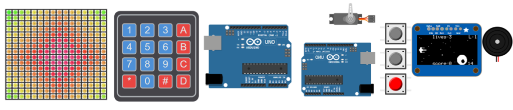
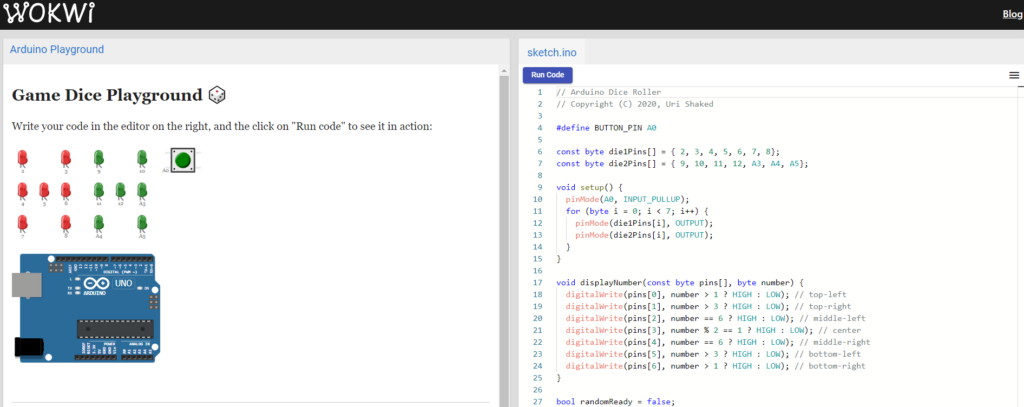
Have you ever wanted to simulate an Arduino? Either for convenience or to ensure the project works before implementing it or even buying the components, a simulator is an extremely welcome (and useful) tool, especially if it’s just right there, in your browser. With that said, Wokwi.com’s Arduino Playground is here to help you!
Arduino Playgroud is a free Arduino simulation tool in the browser, where you can write your own sketches in it and use it with other components, such as LED’s, buttons, displays (from seven segments to OLED’s), potentiometers, among others. It also allows you to monitor the I2C and serial peripherals. You are not very limited in terms of them, as there is already a rich set of components, with new additions coming all the time, where you can also request your favorite ones to be added. Aside from writing your own sketches, both the libraries and components come with multiple examples, so you’re not lost there. Besides the technical components themselves, you can also try some games and example projects, such as the traffic light, the Simon game, and my least beloved, the spaceship game. Try it, you will know why.
Left to right: NeoPixel matrix, keypad, servo and the spaceship game, all available in the Arduino Playground
Jokes aside, you can modify the code, tinker with all the simulated components and experiment with the libraries that you intend to use, to then see the results almost immediately in your browser without any hardware or even extra software. This is specially useful if you want to speed up the development of your project, by ensuring it works even before your components have arrived.
The interface is clean, providing you with your virtual components and the Arduino sketch side by side, which can also format your code and upload it to a real Arduino (in Beta). Since the website is mobile-friendly, you can even code on the road, always a nice touch. Unfortunately, you are unable to share or save your tinkered projects or bookmark/save them online for future use, but will soon be added to the already feature-packed playground. From an electronics simulator perspective, it would be nice to have current and voltage measurements. More features will be added soon, as this ongoing project seeks actively for the feedback of the Arduino community.
Performace-wise, the sketches run seamlessly without any issues. The Arduino simulator runs over the emulated AVR8jscore implemented in Javascript, meaning that every instruction is executed, not just simulated, making it a blazing fast experience. The emulator is downloadable via the NPM package manager, which means that you are free to try it out in your own Javascript projects.
The Arduino Playground’s interface
Right now, Wokwi is a very promising Arduino simulator, and it only looks like it’s gonna get better!


.png)