fpx is a tiny & easy to configure module that enables use of USB‑C (USB‑PD) chargers, adapters & power banks as power sources. It can be added to existing devices to expand the ways they can be powered (from a USB-C car adapter, power bank, etc.) and not just the power brick they came with. It can also be used in new projects to easily access up to 100 watts of safe and clean power from existing USB-C adapters.
Features
Configure (and reconfigure) in a few seconds using any smartphone, tablet, workstation/laptop running Windows, Mac or Linux. Arduino and your projector will do too!
Up to 100W (20V @ 5A) output.*
Voltages: 5V, 9V, 12V, 15V and 20V.*
Currents: 0.5A‑5A in 0.25A steps.*
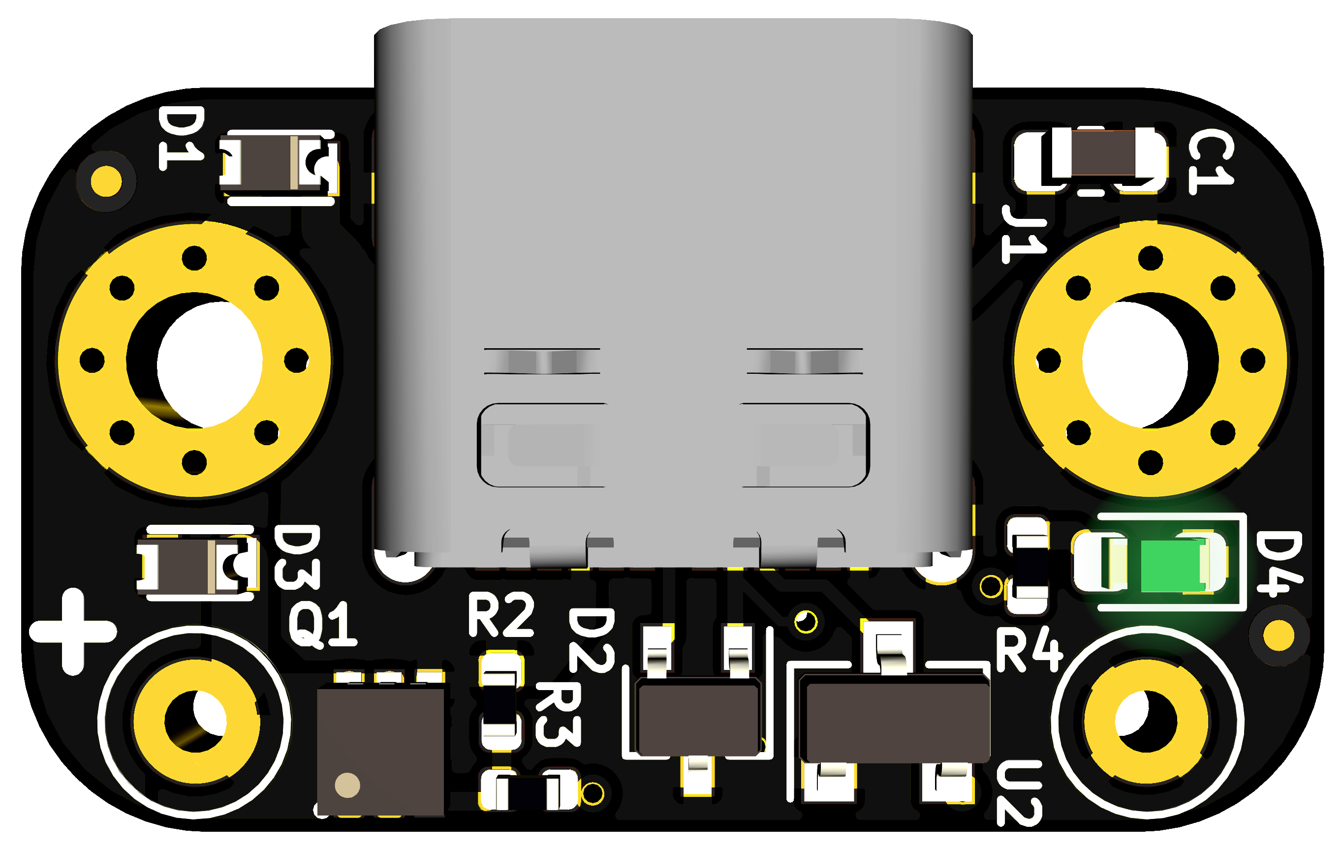
M2 mounting holes.
Reverse voltage, over-voltage & ESD protection on USB pins and output terminals.
Supply line discharge on cable detachment and voltage changes.
Supply voltage monitoring and auto‑shutoff (protection against malicious or misbehaving sources).
Expand the type of projects you can do with easy and safe power up to 100 watts.*
Power your devices by your car adapter and on the go with a power bank, instead of only with the wall adapters they came with.
Power more of your portable devices with a single adapter when travelling.
One set of USB‑C adapters means backup power for every USB‑C powered device you have.
Re‑use your high quality USB‑C adapters and save space storing random bricks and save time looking for them.
Freedom to pick what length of cable to use at any given time.
Replace damaged cables only, not entire adapters.
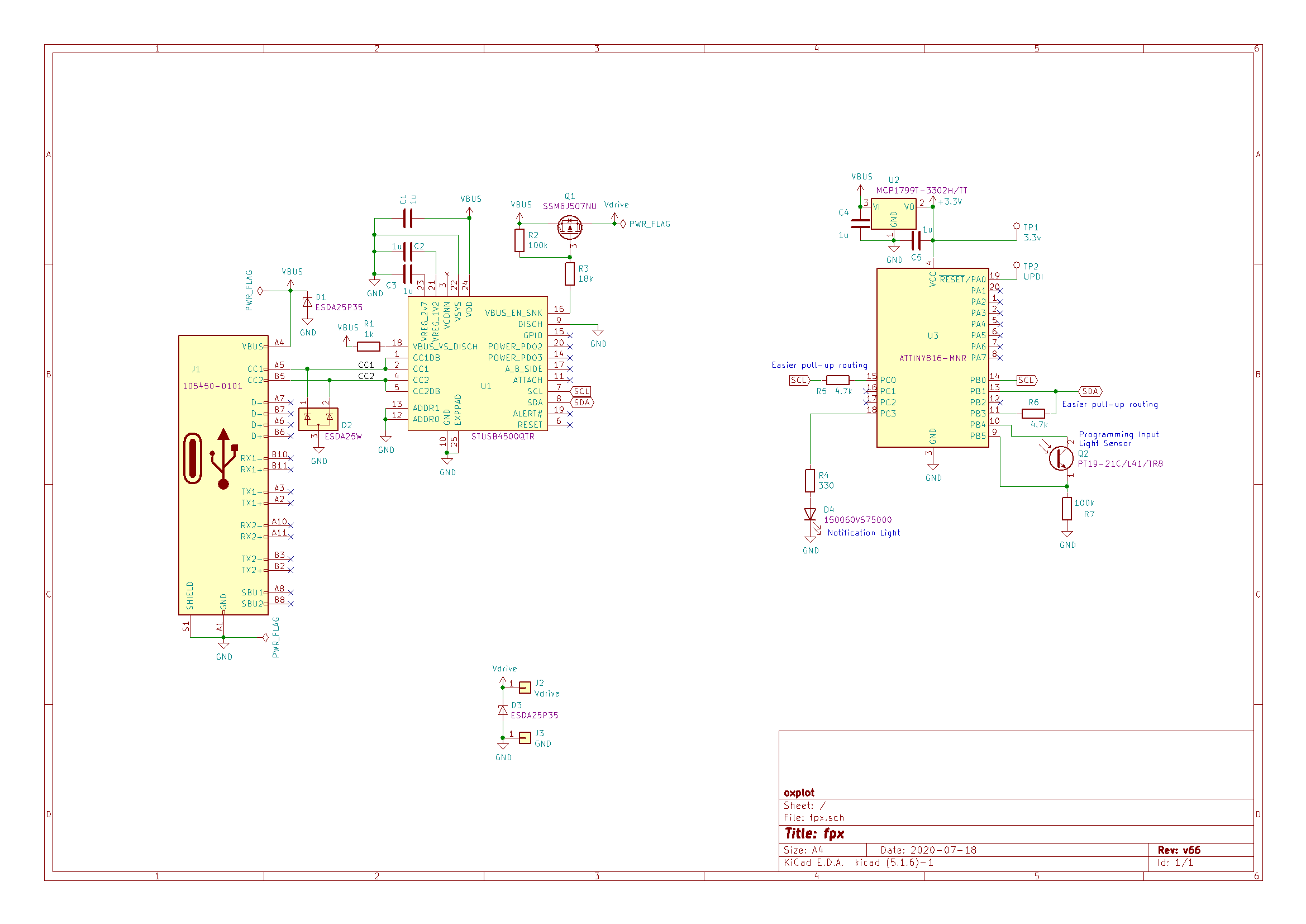
Schematic
fpx board is designed using the amazing KiCad. The design files here are ready for manufacturing and they include part numbers as well.
Programmer
Firmware for fpx is written in C in the standard environment provided by Atmel via their Atmel Studio IDE on Windows. It should be possible to both compile and program this firmware using free and open source software such as GNU toolchain and avrdude on linux and other platforms. The firmware code is written as a single C file with no external dependencies which should make porting it easier.
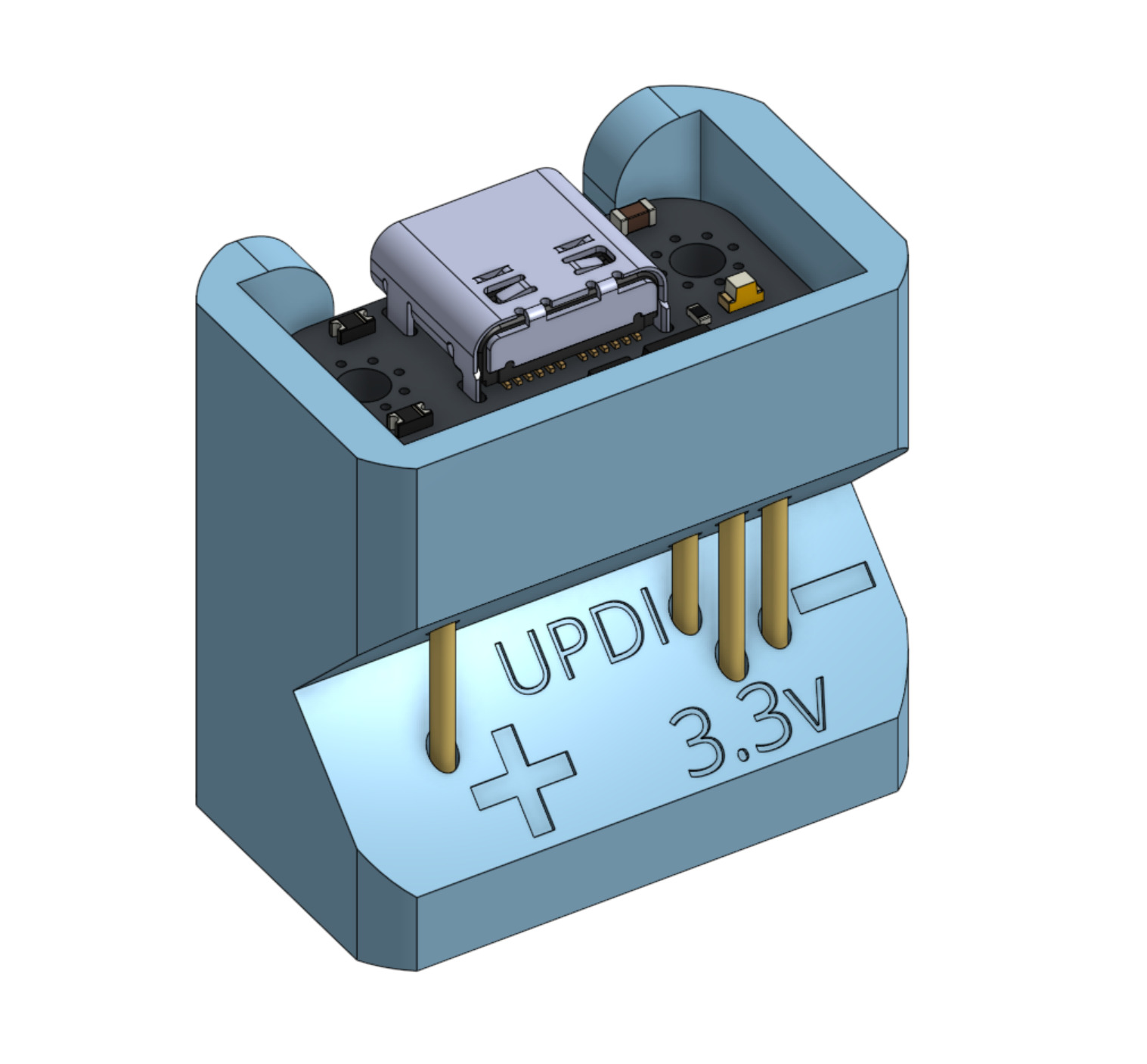
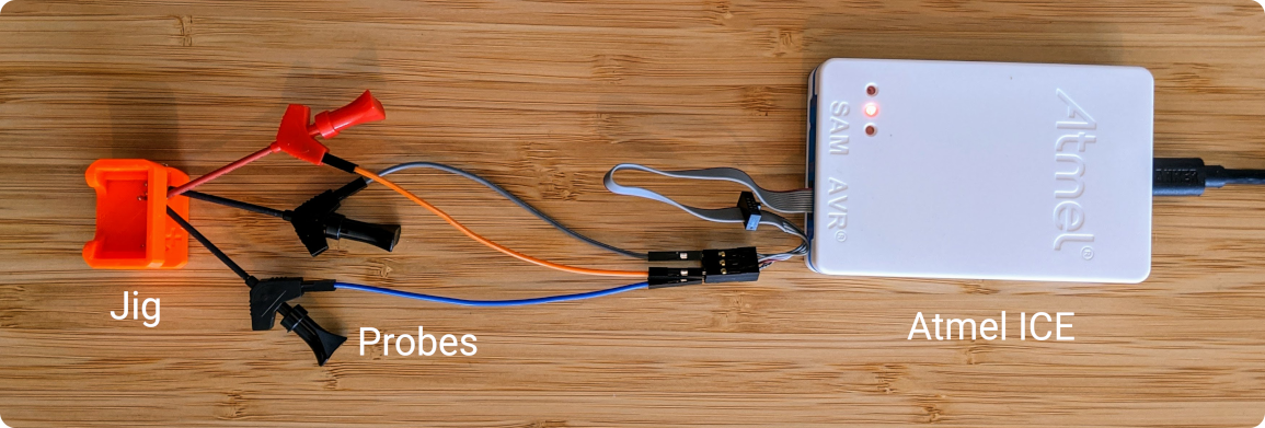
fpx runs on ATtiny816 which is programmed over a single wire UPDI interface. It can be programmed and live debugged using Atmel ICE. fpx exposes UPDI, along with output of the 3.3v linear regulator as test points. Together with the ground terminal, it’s all that’s needed to
program and debug the board using Atmel ICE.
A very rudimentary jig is provided in [STEP](./fpx_rev66_prog_jig.step) and [STL](./fpx_rev66_prog_jig.stl) formats, suitable for pogo pins with body diameter of 1 mm and compressed length of 14.5 mm.
The source model is [a public onshape document] which you can copy and make modifications to. You will need a free onshape account to make changes. The model can be 3D printed using extrusion printers such as Prusa i3, without the need for overhang support.
Adjust camera position with the right mouse button.
Double-click to enter the fullscreen mode.
On mobile devices swipe to rotate.
On mobile devices pinch two fingers together or apart to adjust zoom.
On mobile devices 3 finger horizontal swipe performs panning.
On mobile devices 3 finger horizontal swipe performs panning.
The body of pogo pins is exposed on the side of the jig. You will need clamp-type test probes or similar to make connections to the programmer as shown below:
Availability
Purchase ready to use modules for $20 on Tindie.com
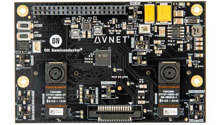
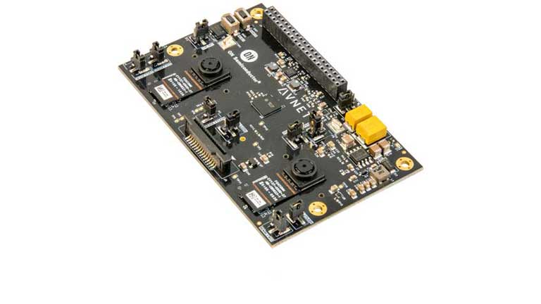
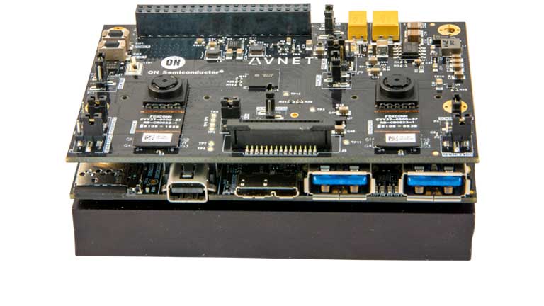
Global technology solutions provider, Avnet, introduced the 96Boards ON Semiconductor Dual Camera Mezzanine development and prototyping platform for the AP1302 imaging processor, coupled with dual imaging camera modules. According to the company, the platform will enable design and system engineers to create cost-effective embedded vision applications utilizing industry-standard technologies.
The two Imager Access System (IAS) camera modules that ship standard on this Mezzanine use the AR0144 monochrome digital image sensor from ON Semiconductor. The AR0144 is a 1-megapixel Mobile Industry Processor Interface (MIPI) sensor (1280 horizontal by 800 vertical resolution) and will run at 60 frames per second at full resolution. Its global shutter pixel design is designed for accurate and ideal capture of moving scenes while producing digital images. The ability to capture clear images is ideal for applications such as scanning, industrial inspection, and drone navigation.
By using the 96Boards standard, this card can enable low-latency vision system prototyping by leveraging capabilities of the Xilinx Ultra96-V2 platform.
The platform utilizes MIPI and the camera serial interface (CSI2) standardizations which are specifications of the MIPI Alliance. The MIPI-CSI2 specification defines the interface between the image sensors, ISP, and a host processor, and is used for high-speed communications output from image sensors in most embedded systems.
The API 1302 image co-processor from ON Semiconductor performs image processing functions within the platform, including turning, configuration, and calibration of the sensors. These processing functions also help to reduce the design efforts of developing an embedded camera system. The AP1302 interfaces the sensors and the host processor using MIPI-CSI2 lanes.
The IAS image sensor module interface from ON Semiconductor helps solve this problem and enables:
Simplified camera system design: A single, standardized interface helps to connect the imaging module to the processing board, such as the 96Boards Mezzanine.
Shorter lifecycle: Solution decreases time to market by enabling low-touch design.
Lowered learning curve: Prior imaging system expertise is not required since IAS is a plug-and-play solution.
The purpose of the standardized IAS interface is to help any embedded vision system or board designer to gain access to all compatible image sensor modules.
The Avnet-designed 96Boards ON Semiconductor Dual Camera Mezzanine development and prototyping platform comes with two IAS sensor modules and an AP1302 imaging co-processor. It is available today in the Americas, EMEA, APAC, and Japan for $199 (USD).
Renesas’ reference design considers the thermometer’s range of operation, accuracy, power considerations, and display options.
Renesas’ winning combination IR contactless thermometers are needed for medical applications to monitor an individual’s body temperature before entering any public place. Depending on the target market and application, the thermal range to be monitored, as well as the required accuracy, may differ significantly. This is especially the case when comparing thermometers used in a medical environment versus those used in industrial applications.
This reference design considers the thermometer’s range of operation, accuracy, power considerations, and display options. The design is one possible use case for designers.
Features
RL78/I1D microcontrollers (MCU)
Ultra-low power analog 16-bit MCU
Suitable for applications such as detectors and sensors requiring low power and analog integration
Enhanced analog functions, such as operational amplifiers, a 12-bit A/D converter, and window comparators
Supports very low power operation (124 µA at 1 MHz) and a high-speed 4 µs wake up
RL78/I1B MCU
High precision low power analog 16-bit MCU
Low power MCU with 24-bit ΔΣ A/D converter
RTC backup and high-accuracy oscillator
Ideal for the electricity meter
ISL9205 Li-Ion battery chargers
Single-cell Li-Ion/Li-polymer battery charger
Operates as a pulse charger, where the charge current is determined by the current limit of the AC adapter during the constant current phase
Operates in a linear mode during the constant voltage phase in both adapter.
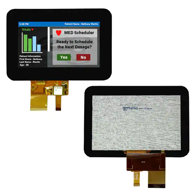
Newhaven Display’s effortless EZ Grip IPS TFTs make mounting easy with sleek, simple designs
Newhaven Display’s 4.3″ EZ Grip TFTs deliver high-quality images and reliable performance with a built-in mounting interface for simple installation and sleek, seamless integration in applications. These 4.3″ displays are equipped with IPS technology to bring a wide range of viewing angles and accurate color representation on TFT LCDs.
These 4.3” TFTs are ideal for integrated displays in any lighting conditions. The EZ Grip design allows the display to sit flush with its application when mounted, allowing for easy installation and a streamlined appearance.
Features
EZ grip mounting
4.3″ IPS TFT
Built-in controller
High-brightness LED backlight
800 x 480 pixels
RoHS compliant
Optically-bonded capacitive touch panel with I²C interface
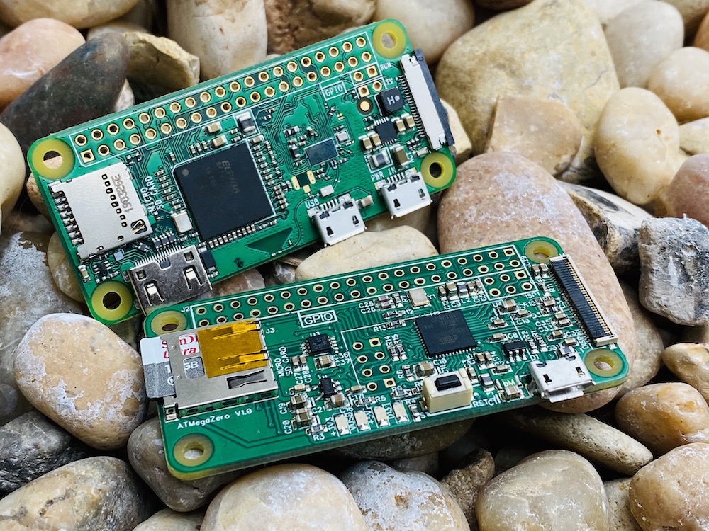
The small form factor of the Raspberry Pi Zero has now been brought to the Arduino World!
An Arduino Leonardo compatible board with a strikingly simillar shape to the well-known Raspberry Pi Zero is available on GroupGets for $24.99, but you will have to hurry up to get your hands on this item, as the good buying campaign is expected to end by September 30.
The ATMegaZero may look similar to the Raspberry Pi Zero, but they are actually quite different in specs, where the Arduino board’s specs are:
ATmega32U4 microcontroller core (clocked at 16MHz)
32KB Flash, 2.5KB SRAM and 1KB EEPROM memories
40-pin GPIO header (17 Digital I/O’s, 6 Analog Inputs, 8 GND pins, 2 +3.3V pins and 2 +5V pins)
2 ESP-01 GPIO pins
Micro SD Card module for reading and writing data
32 pins OLED Display port (compatible with 30 pinsSSD1306& SSD1331)
Pinout for connecting an ESP-01 WIFI Module
UART, SPI and I2C communication
7 PWM channels
5V operating voltage
Micro USB port and 6-pin ICSP (In-Circuit Serial Programming) header, for power, programming and debugging purposes
1.5oz weight
65mmx30mm dimensions (2.6″x1.2″)
As you can see, the looks are quite deceiving, as the ATMegaZero does not run linux or run your computer vision programs, but it still can be regarded as a welcome addition to the Arduino family. The designers describe it as “designed with makers in mind” and guarantee it works out of the box with the Arduino IDE. There is also a resource-packed website, where more detailed information can be found, including a pinout, setup instructions and other necessary technical details that are available, to help you get started.
Along with the board, you can order some add-ons with it, including a protoboard with the same shape as the ATMegaZero and headers for it.
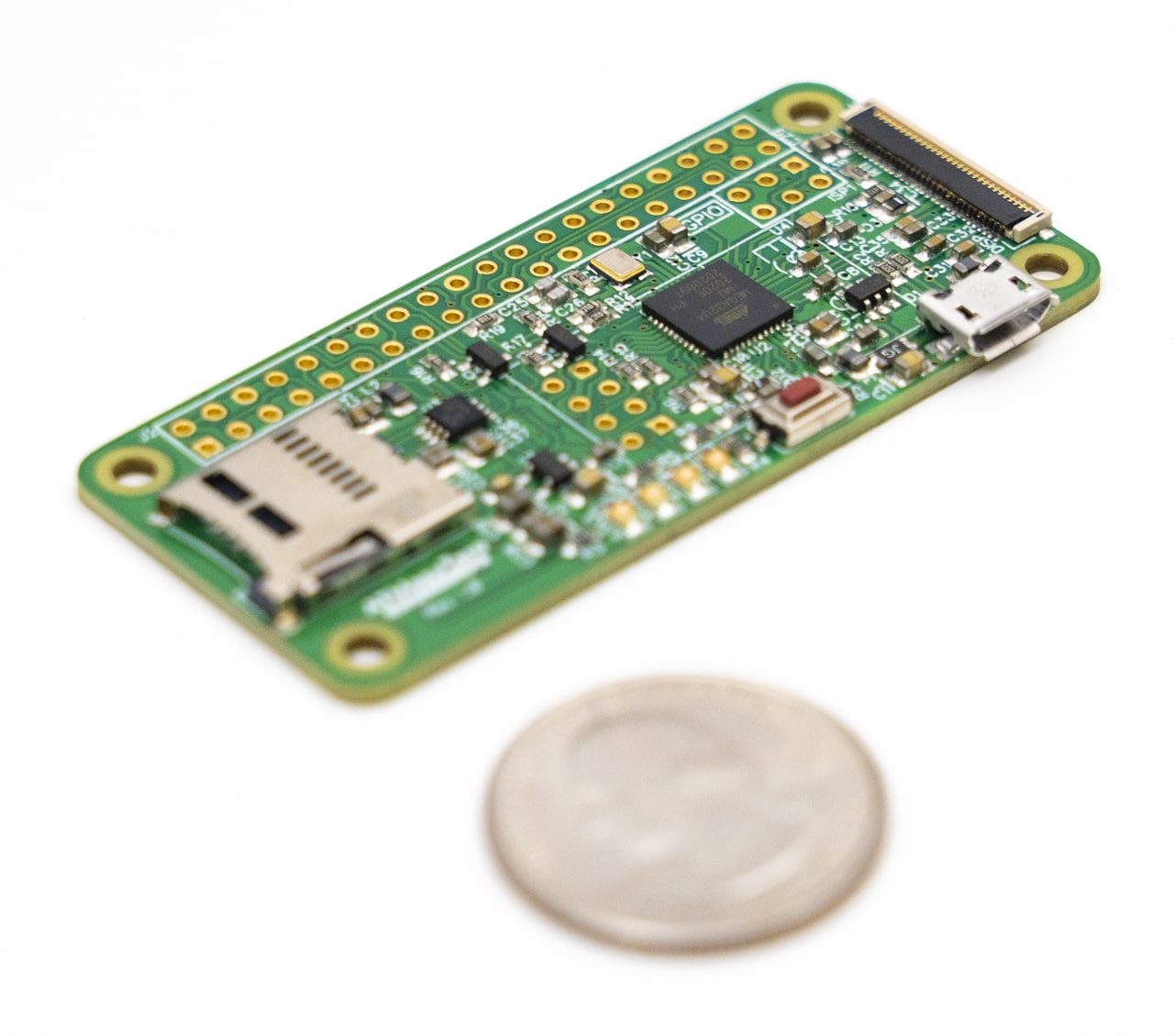
ATMegaZero’s size when compared to a coin
Regarding it as a maker’s perspective, what can you do with it? Well, a lot! Besides the SD card module in the board, it also provides an easy connector to an OLED display and an ESP-01(s) Wi-Fi module, while achieving this small form factor. Of course, this is not directed to be a Raspberry Pi competitor, but the potential is there. You get a lot of possibilities for such a small size. It can also be paired with the Raspberry Pi Zero cases, since their modeling is that similar, which means you don’t have to fool around with 3D software to provide a casing to your project, at least for once.
To this date, the Hackster launch campaign counts with 51 of 100 target backers, which is expected to fill by the end of the month.
Will you pick this board up? What would you make of it?
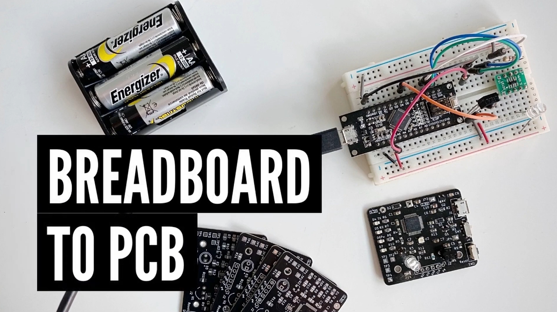
In Sayanee’s Basu’s video, we can look at the design considerations in the process of taking a breadboard prototype to a custom PCB, from the microcontroller to the various subsystems, to the power, the bootloader, and even how to deal with faulty components.
A breadboard can be useful for educational purposes, art projects, and even small testing. However, when we need multiple units or the components required are only available in SMD or other non-standard packages, a PCB is mandatory. Another advantage of a custom-made PCB is the capability of producing smaller and more robust units in higher quantities, which leads to a better project overall.
The first design consideration is the microcontroller. Developing a schematic can be intimidating at first, but when you look at some open-source designs for the same MCU and the datasheet, you will feel more comfortable. This is also the step where you choose the package and the variant of the microcontroller you will use, using the datasheet’s ordering information section for guidance. Lastly, you should make sure to check the availability and stock from the vendor before doing the layout.
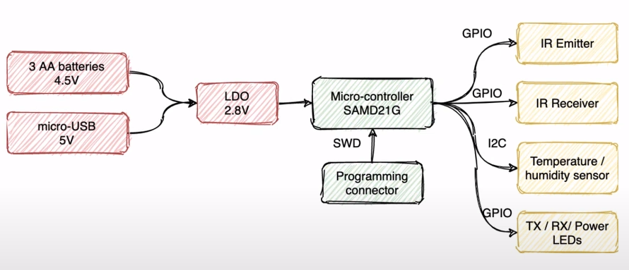
After choosing your microcontroller, you should look at the subsystem level, dividing the breadboard prototype into the different sections. DrawIO can be used to draw some quick flowcharts and connect the subsystems. You can also divide subsystems into 3 different colors, according to their category: power, microcontroller and sensors/actuators. Every box in your subsystem can later become a logical block in your schematic, separating the major functional areas of your system. You can also use solder jumpers or zero-ohm resistors in order to separate the functionalities of these subsystems, which can be useful to test each individual subsystem individually.
Diagram of the different subsystems (red – power; green – microcontroller; yellow – sensors/actuators)
The next thing to take into consideration is power. You need to decide how your PCB is going to be powered, which can range from USB, alkaline, LiPo, or other types of batteries, or even a coin cell. You can even use more than one, but keep in mind extra circuitry may be required, otherwise, you can damage your entire PCB. Here, you can use online research and simulation to guide you. After deciding the power sources, you must choose a voltage regulator for the MCU, where you should refer to the microcontroller datasheet and look for the operating voltage and current, and then choose one that fits the criteria. Make sure to also check the maximum ratings of all the components, to ensure their compatibility with the rest of the circuit. You can also create a power tree, illustrating the main power flow through a tree of power converters that convert the supply power to the voltage and current required to drive the various loads. You should also consider incorporating a power switch, which can come in handy to debug, and a reverse-polarity protection circuit, which in its simplest form is a Schottky diode.
The next design consideration is the bootloader, which is important to upload the firmware you developed into the MCU, which will come bare from the factory. To this, you should refer the available interfaces in your MCU datasheet, along with the pins the said interface connects to. You also need to ensure you have the reset circuit for the microcontroller, which is necessary to upload the code into your board and to reset the board. This is often one of the scariest parts because it generally can’t be performed on the development board.
The last things to take into consideration are the sensors and the actuators. You should browse the datasheet of each of them to check at least the reference application circuit, to then replicate it into your PCB. To detect faulty sensors/actuators or even a design error, you should populate 2 or 3 PCB’s, because if one of them is working, then you can assume faulty component, but when none work, then you should review your design, because there may be something wrong with it.
Lastly, you can optionally include some LED’s on the power and bootloader pins, for debugging purposes, in your first prototype.
Hopefully, these tips will lead you to better PCB’s, the ones that work on the first try!
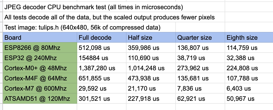
For most firmware developers and hobbyists, who have had to write firmware for projects that involve displaying JPEGs on an LCD with an Arduino, one thing that quickly comes to mind is the bulkiness of the libraries and the slow speed at which the images are displayed. While the speed is usually due to the low memory and processing speed of the microcontrollers in use (8-bits microcontrollers), the bulkiness is usually as a result of the schemes and tricks that were adopted to get the low performing MCUs to perform better with jpeg display.
While things have improved in recent times, with 32-bits high performing MCUs with increased RAM and processing speed now available, there has been little or no change to the efficiency/performance of Jpeg libraries. To ensure change and growth is also experienced with the libraries, Software Optimization Specialist, Larry Bank, recently decided to give the libraries the necessary facelift via the release of his new library: the JPEGDEC library.
The new library which targets the Cortex-M0+ processors or any chip with a minimum of 20Kb of RAM is designed to make the display of JPEGs faster on boards based on the Cortex-M0+, or any chip with a minimum of 20K of RAM (bare minimum requirements), without sacrificing the memory of the boards for speed.
Acknowledging the prior existence of different JPEG Libraries for the Arduino, including the ones written by him, Larry, while sharing the rationale behind the new library in a recent blogpost, mentioned the existence of more processing power on MCUs as a motivating factor for the development. He said, While it’s possible to decode JPEGs piece by piece with some intelligent code under the conditions presented by 8-bit systems, it’s possible to go much faster when you’ve got a little more headroom, and this new library was merely doing that, from eliminating unnecessary marker checks to ignoring unneeded data for scaled-down outputs, all coming together to give a faster result.
Highlight features of the new library as noted by Larry includes:
Supports any MCU with at least 20K of RAM (Cortex-M0+ is the simplest I’ve tested)
Optimized for speed; the main limitation will be how fast you can copy the pixels to the display. You can use DMA assisted SPI to help.
JPEG image data can come from memory (FLASH/RAM), SDCard or any media you provide.
Simple class and callback design allow you to easily add JPEG support to any application.
The C code doing the heavy lifting is completely portable and has no external dependencies.
Includes fast downscaling options (1/2, 1/4, 1/8).
Includes option to detect and decode the embedded Exif thumbnail
Supports Baseline Huffman images (grayscale or YCbCr)
Includes optional Floyd-Steinberg dithering to 1, 2 or 4-bpp grayscale output; useful for e-paper displays
The library has already been taken for a spin by several notable community contributors like Paul Stoffregen who made a Youtube Video to demonstrate the performance of the library. Larry himself also developed a benchmark test sketch which shows the library’s performance across different development platforms.
More information on the library and its performance are available on the project’s Github page.
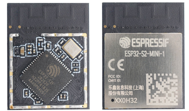
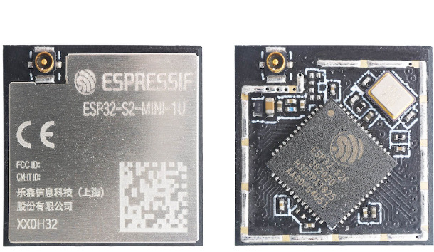
Espressif systems has announced ESP32-S2 MINI-1U with IPEX antenna and ESP32-S2-MIN-1 with a PCB antenna the breed of a newly branded ESP32-S2 WIFI modules part of Mini series modules. These are new additions to the catalog of Espressif systems which includes the ESP32-S2 Development boards, Espressif’s ESP32-S2 Wi-Fi Soc with future release of ESPS32-S3 and ESP32-C3 processors and much more both in software and hardware. The company describes the two modules as “two powerful, generic Wi-Fi MCU modules with a rich set of peripherals.” The two modules are only different in size and antenna type, but share similar specs.
ESP32-S2 MINI-1U
At the core of the ESP32-S2-MINI modules are ESP32-S2FH4, which is an Xtensa® 32-bit LX7 CPU that operates at up to 240 MHz. This chip has a low-power co-processor that can be used instead of the CPU, in order to save power while performing tasks that do not require much computing power, such as the monitoring of peripherals. ESP32-S2FH4 has up to 43 GPIOs and integrates various peripherals, such as SPI, I2S, UART, I2C, LED PWM, LCD, camera interface, ADC, DAC, touch sensor, and temperature sensor. ESP32-S2FH4 also includes a full-speed USB On-The-Go (OTG) interface which enables USB communication in any place, at any time. The modules are the ideal choice for a wide variety of application scenarios relating to the Internet of Things, wearable electronics, and smart home.
The following are the ESP32-S2 mini-modules specifications:
With no external flash, the module can be made smaller with the flash embedded inside the processor. The two new modules are the first among more modules to come. Espressif Systems are also planning to bring us two development kits namely ESP32-S2- DevKitM-1 and ESP32-S2-DevKitM-1U with no official release date. The ESP32-S2-MINI modules are scheduled for mass production for December 2020 and are currently undergoing FCC, CE, and SRRC certifications. The completion date for the above-mentioned certifications is expected at the end of November 2020. The Company urges customers to request samples if there is a specific project to run.
Regarding the ESP32-S3 and ESP32-C3 Processors little information is available. With the information gathered, ESP32-S3 is looking like a multicore processor clocked at 240MHz with WiFi and Bluetooth support, SPI Fflash, SPI ROM, and likely AI instructions.
The previous tutorial about the non-inverting operational amplifier has shown all the details of this op-amp configuration that takes the input signal on the non-inverting pin (+). This could be done by studying the ideal and real models and demonstrating all the important formulas. In this new tutorial, the same approach will be proposed for the inverting operational amplifier in which the input signal is supplied to the inverting pin (-) of the op-amp.
As a result, the ideal model will be detailed in the first section where the expressions of closed-loop gain, input, and output impedances are proven and discussed.
The second section deals with the real model for inverting op-amp, in which parasitic phenomena change the expressions of the important parameters mentioned above.
Examples of circuits based on an inverting op-amp are presented in the third section. This will highlight their role and possible uses in electronics.
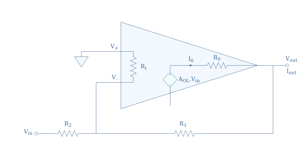
Ideal inverting op-amp
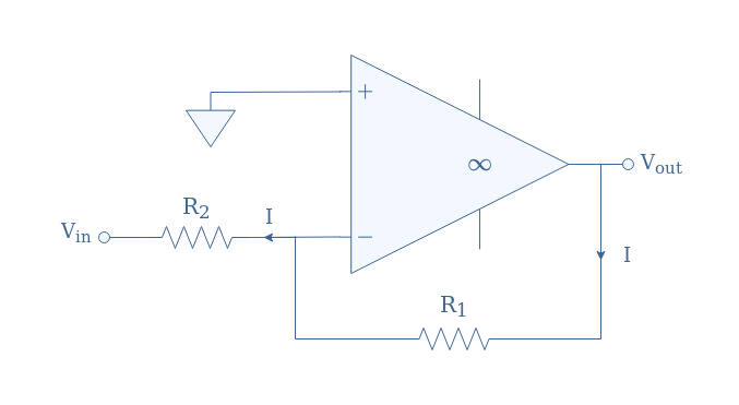
In an inverting op-amp configuration, the negative (or inverting) input labeled with the sign “-” receives both the input signal Vin and the feedback loop. The positive (or non-inverting) input labeled with the sign “+” is simply connected to the ground.
An inverting op-amp configuration is presented in Figure 1 below, for which the symbol “∞” highlights that the circuit is ideal.
fig 1: Ideal inverting op-amp circuit
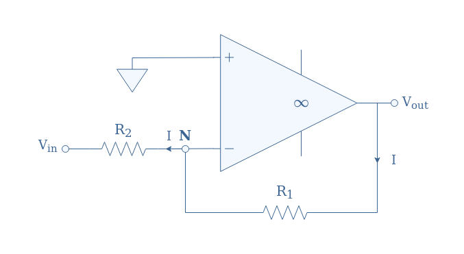
For the ideal configuration discussed in previous tutorials, it is assumed that no currents can enter either the non-inverting or inverting inputs, therefore, the feedback current I is found across R1and R2.
This is directly a consequence of the fact that we assume the node N to be a virtual earth and this results in particular to the equality V+=V–=Vin.
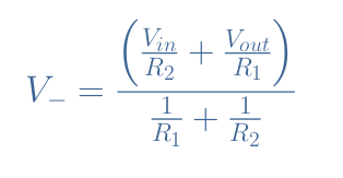
However, since the non-inverting input is connected to the ground, V+=0 , also implies V–=0. In order to get an expression for V–, we can use Millman’s theorem, which is a particular form of Kirchoff’s current law. The voltage signal at the inverting input can therefore be written according to the equation below:
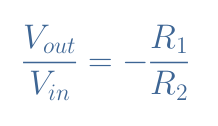
Since V+=V–=0, the above expression is also equal to zero. This can only be true if Vin/R2+Vout/R1=0, we can rearrange this expression to write the closed-loop gain (ACL) of an ideal inverting op-amp such as shown in Equation 1:
eq 1: Closed-loop gain of an ideal inverting op-amp
We can note that the closed-loop gain is strictly negative and can approach zero. This means that the output signal is inverted (the phase shift is 180°), thus the name “inverting op-amp”. Moreover, this configuration can amplify the signal if |ACL|>1 or reduce its magnitude if |ACL|<1.
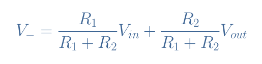
Real inverting op-amp
The circuit diagram of a real inverting op-amp is presented in Figure 2:
fig 2: Internal equivalent circuitry of a real inverting op-amp
Such as we had done for the non-inverting configuration, we will now properly demonstrate the formulas for the closed-loop gain, input and output impedances for a real inverting op-amp.
Closed-loop gain
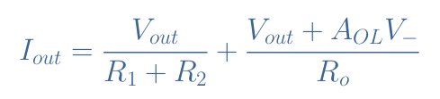
We begin the demonstration of the closed-loop gain by writing that Vout=AOL(V+-V–). Such as mentioned in the first section, the equality V+=0 is still valid because of the ground connection, this implicates that V–=-Vout/AOL.
In the non-inverting op-amp, V– could moreover be written as the result of a voltage division by the series configuration R1-R2. However, in the inverting op-amp, V– is rather expressed by a superposition of Vout and Vin:
In this formula, we can replace V– by -Vout/AOL, therefore we get:
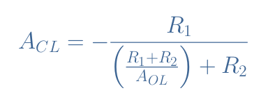
We can finally express the ratio Vout/Vin in Equation 2, which is the definition of the closed-loop gain ACL:
eq 2: Closed-loop gain of a real inverting op-amp
It is interesting to note that if the op-amp approaches its ideal model, AOL→+∞ and therefore Equation 2 can be simplified back to Equation 1.
Input Impedance
For an inverting configuration, the input impedance is simply expressed by Zin=R2, whether the op-amp is considered real or ideal. This observation is directly a consequence of the fact that the potential V– at the node N is equal to 0.
Output Impedance
In order to demonstrate the expression for the output impedance, we need to short the resistance R2 to the ground. First of all, we assume that no current enters the op-amp through the inverting and non-inverting inputs. Even if it is not exactly true, the several orders of magnitude difference justify this choice. This means that the current through R1 and R2 is the same and can be expressed by Vout/(R1+R2).
The current IRo across Ro can simply be expressed by performing a Kirchoff’s voltage analysis in the output loop simultaneously with the Ohm’s law formula:
Note that -Vin can be replaced by V– because the non-inverting input is directly connected to the ground.
The output current Iout is given by the sum IR1+IRo:
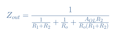
Since V– can simply be expressed by IR1×R1, we can inject this expression in the above formula. After factorizing by Vout every member in the right side of the expression of Iout, we can write the ratio Vout/Iout which defines the output impedance Zout of the configuration:
eq 3: Expression of the output impedance for a real inverting configuration
We can again emphasize that this expression is consistent with the ideal model, indeed when AOL→+∞ we get Zout=0.
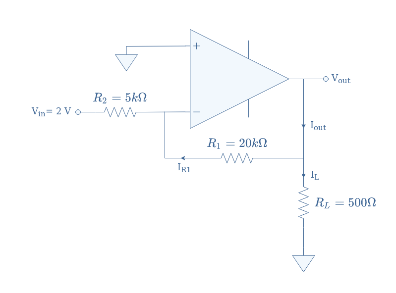
Inverting op-amp example
Consider the following inverting configuration presented in Figure 3 for which we will compute the closed-loop gain, input, and output impedances:
fig 3: Example of real inverting configuration
We need to remind that in most of the cases, the open-loop gain AOL is sufficiently high so that the ideal formula can directly be used for the calculation of the closed-loop gain ACL. This value is therefore given here by ACL=-R1/R2=-4.
Since Vin is given to be equal to +2 V, the output voltage is simply Vout=ACL×Vin=-8 V. If we still assume that no current enters through the inverting and non-inverting inputs of the op-amp, the current IR1 across R1 is equal to the current IR2 across R2. This last one is given by Ohm’s law: IR2=Vin/R2=0.4 mA.
The current IL across the output load is also given by Ohm’s law: IL=Vout/RL=-16 mA. By applying Kirchoff’s current law, we see that the output current Iout satisfies IR1=Iout+IL⇒Iout=16.4 mA.
Finally, we can say that the input impedance is given by Zin=R2=5 kΩ, the output impedance is given by Zout=Vout/Iout=490 Ω.
Conclusion
When the input signal is supplied to the pin “-”, the op-amp is said to be in an inverting configuration. The design and main properties of this configuration are presented in the first section that focuses on its ideal model.
In the second section, real inverting op-amp circuits are investigated, the demonstrations and exact formulas for the closed-loop gain and impedances are different and more complicated due to parasitic phenomena modelized by resistors.
However, in most cases, the real op-amps can be assimilated to their ideal model since the open-loop gain has always a value that is high enough to justify this choice.
An example of real configuration is shown in the last section, we present how to calculate the main characteristics of a configuration with the knowledge of the resistors value and input voltage.
Inverting and non-inverting configurations present very similar characteristics such as high input impedance and a low output impedance. The main difference comes from the closed-loop gain, which can only be strictly positive and higher than the unity for the non-inverting op-amp but strictly negative for the inverting op-amp.
The non-inverting op-amp will therefore always amplify the signal and keep it in phase, the inverting op-amp, on the other hand, inverts the phase and can either amplify or decrease the magnitude of the input voltage depending on the resistor values present in the feedback loop.
Differential current probe with single-ended output, +/-18 V supply voltage, 6 MHz bandwidth, and gain of 2, set by a single resistor, can be increased. Designed by A. Rosenkränzer
This current probe has a differential input and single ended output. Instrumentation amplifier AD8421 is used for its high bandwidth. The amplifier is configured for a gain of 2, set by a single resistor R5: G = (9.9 kΩ/R5) + 1. Bandwidth at this gain is greater than 6 MHz, measured bandwidth is about 8 MHz. Even at a gain of 100 bandwidth of the AD8421 is still 2 MHz. Have a look at the datasheet for more information. The input filters (R1/C1, R2/C2) provide a simple overvoltage and transient protection for short overload conditions and correct the increase of gain of the AD8421, close to the cutoff frequency, to straighten the amplitude vs frequency characteristic of the probe. Although the AD8421 has very robust inputs, long overvoltage conditions should be avoided. Input voltage range is limited by the +/- 15 V power supply (onboard regulators), a little over +/-12 V. The probe has its own voltage regulators and a common mode choke to suppress possible interferences from the DC power supply used for the probe (think of SMPS versions). A symmetrical laboratory power supply can be used or a small transformer with full wave rectifier and smoothing capacitors. D3 and D4 protect against wrong polarity, they’re not meant for rectifying an AC voltage! LEDs LED1 and LED2 indicate both power supply voltages are present, and the probe is active. Two extra resistors of 10 MΩ (R3, R4) have been added to the inputs so these stay biased and the output remains at ground level when nothing is connected to the probe.
Free Elektor Article: Differential Current Probe – [Link]