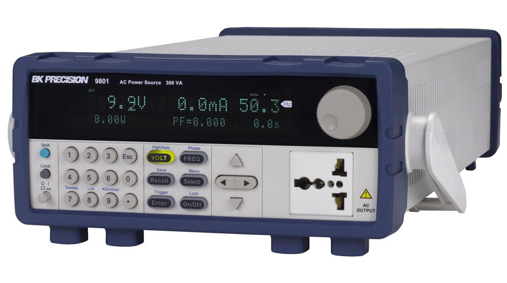
The BK9801 is a programmable AC Power Source and measurement tool delivers a maximum of 1500VA through the universal line output terminals on the front and the output connector on the rear. The output can be varied from 0 to 300V with 0.1V programming resolution. The output frequency can also be adjusted from 45 to 500Hz with start and stop phase angle from 0 to 360°. The bright VFD display shows Vrms, Irms, Ipeak, frequency, power factor (PF), apparent power, true power and elapsed output time. The AC source provides a power line disturbance (PLD) simulator, list mode and sweep mode for simulation of common power grid faults and disturbances. A built-in dimmer function is also available for testing motors and LEDs. It is suitable for evaluating transformers, TRIACs, SCRs and passive components as well as production, R&D, service and pre-compliance testing.
Specifications:
Adjustable phase angle control
Built-in PLD and dimmer simulation
Voltage and frequency sweep mode
Pre-compliance testing for voltage dips & frequency simulation according to IEC61000-4-11/4-14/4-28 common applications
Downloadable LabVIEW driver and soft panel software for remote control
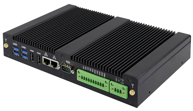
IBASE Technology Inc., a world leader in the manufacture of industrial motherboards and embedded systems, has unveiled the ASB200-918 series based on the IB918 3.5-inch form factor SBC supporting AMD Ryzen SoCs (V1605B/V1202B/R1606G/R1505G). The four models in the series bring together the powerful performance of the “Zen” CPU and “Vega” GPU architectures to deliver a new class of embedded solutions.
IBASE leverages the high performance and stunning graphics capabilities of AMD Ryzen Embedded processors with its own manufacturing flexibility to design the fanless ASB200-918 that runs two simultaneous HDMI 2.0a displays at Ultra HD 4K resolution (3840 x 2160) with a frame rate of 60 fps. Measuring 240mm x 162mm x 42mm, it is equipped with rugged components to ensure a reliable and uninterrupted operation in industrial control, factory, kiosks and other space-critical applications.
The robust design of the ASB200-918 comes with 16GB of DDR4-2666 memory with ECC and up to 32GB support. The unit features a 64GB TLC SSD storage, 12V~24V DC wide power input and optional 90W power adaptor. Versatile I/O connectivity is provided by 4x COM, 4x USB 3.1, 1x USB 2.0, 2x GbE and an external GPIO, while expansion is supplied by two M.2 slots for NVMe storage and WiFi or Bluetooth connections. Supported operating systems include Win10, Win10 IoT Enterprise, Win Embedded Standard 8, and Ubuntu 16.04.
ASB200-918 FEATURES:
Fanless system with IBASE IB918 3.5’’ Disk-Size SBC
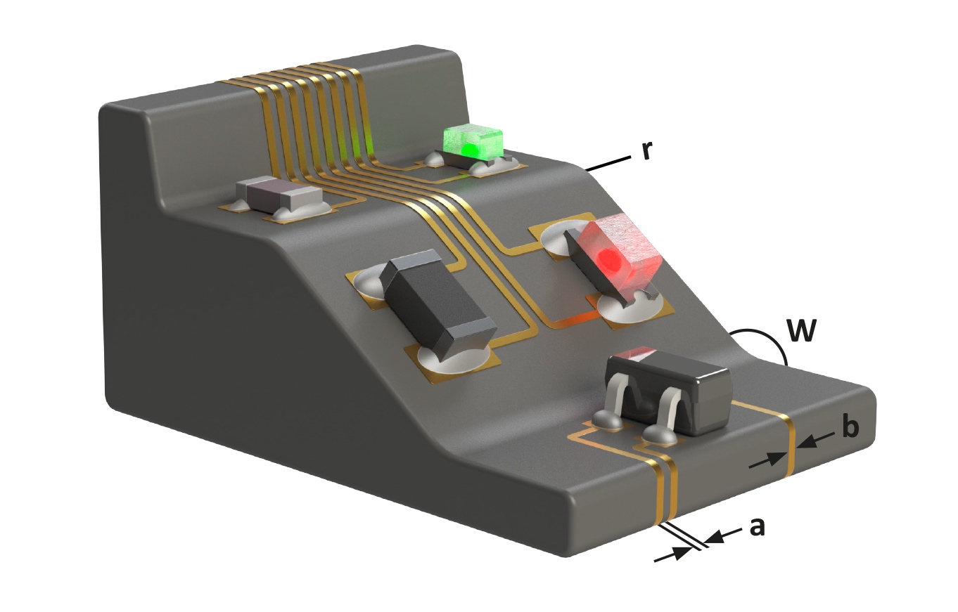
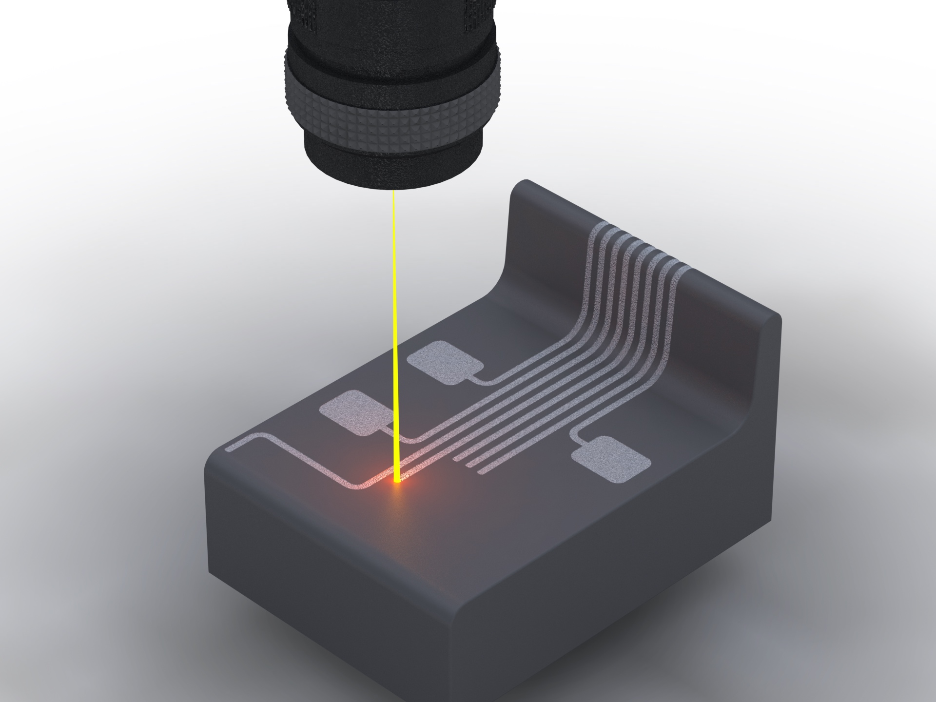
Laser direct structuring (LDS) is a special success story. For almost 20 years, it has been possible to apply electronic conductor paths directly onto plastic parts during series production. Laser Direct Structuring (LDS) – The structure of the conductor path is applied using the LDS process.
LDS enables electronic assemblies to be made in flexible geometric shapes. Smart phones, hearing aids and smart watches are becoming smaller and more powerful thanks to this process.
LDS enables the production of electronic assemblies with flexible geometric shapes. This process enables electronic products (such as smart phones, sensors or medical devices) to become even smaller and more powerful. Automated manufacturing processes also make this process more economically attractive.
There is less and less space available for electronic assemblies, so solutions are needed which replace conventional printed circuit boards. LDS enables further miniaturisation and makes increasingly complex geometric designs possible. This is a stable and reliable process that has established itself in quality-critical sectors such as medical technology or safety-relevant components for the automotive industry.
The LDS process enables three-dimensional assemblies Direct laser structuring enables 3D-MID (Mechatronic Integrated Devices) assemblies to be produced. When using 3D-MID, electronic components can be fitted directly onto a three-dimensional base body, without circuit boards or connecting cables. The base body is manufactured using an injection moulding process, whereby the thermoplastic material has a non-conductive, inorganic additive.
New trends in the LDS process
Several aspects of LDS technology have been improved and further developed over the past few years.
The working area of the laser has been enlarged from 160 x 160 x 80 mm to 200 mm x 200 mm x 80 mm, thus enabling a higher packing density and the processing of even larger components. The working speed of the laser can be doubled to 4 m/s by optimising the servo units and mirrors which guide the laser beam, thereby significantly reducing the processing time. The improvement of the optics enables the use of a laser with a diameter of 100 μm and a laser with a fine focus of 50 μm for processing even smaller structures.HARTING is the only 3D-MID manufacturer in the world that has a laser system with three fine focus optics of 50 μm. Even smaller conductor path gaps can be achieved thanks to this fine focus laser. Thus, many conductor paths can be created on the same component and a higher packing density can be implemented. This is used for safety technology, among other things, because the closely spaced and intertwined conductors are capable of triggering safety alarms from even the smallest physical interference.
Advances in materials and economics
Only specially selected thermoplastics are certified for the LDS process; these are available from stock. The process can be further improved with customer-specific adjustments to the plastic material:
HARTING uses a process which adds LDS additives to non-certified materials to make them MID-compatible. Specific RAL or Pantone colours can be achieved with MID plastics by using colour pigments and special LDS additives. By selecting suitable additives, special RF characteristics can also be implemented, depending on the frequency range.
Component carrier – Electronic components – such as LEDs, ICs, photodiodes and sensors – can be attached directly onto the component carrier. The assembled component carriers can then be processed as standard SMD components.
To further improve the cost-effectiveness of the manufacturing process, HARTING relies on automated robotic systems. The LDS laser system is equipped with a rotary indexing table so that a component can be inserted or removed while another component is still being processed. The in-feed and unloading procedures are automated by HARTING using robotics. This increases throughput and autonomy, while also enabling integration into automated production processes. An additional automation step is provided during the injection moulding process. Here, too, a robot takes over the removal of the injection moulded parts. The use of robotics also improves the precise reproducibility of the processes and, thus, overall product quality.
More growth for 3D-MID
Security caps for payment terminals – The 3D-MID caps protect the electronics from unauthorized access both mechanically and electronically. A highly precise meandering structure detects every access, no matter how small, and consequently prevents theft.
HARTING reports increased demand for MID projects and has further expanded the 3D-MID division by investing in machinery and by acquiring a competitor’s business. Innovative in-house products are also contributing to further growth. HARTING has developed a solution based on 3D-MID technology which replaces flexible PCBs with a component carrier. Instead of using a flex-PCB, the component carrier can be fitted directly with electronic components, thus saving up to two thirds of the cost.
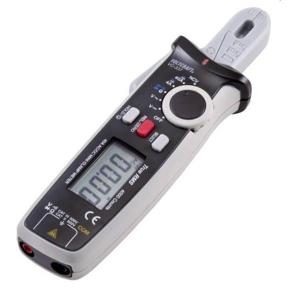
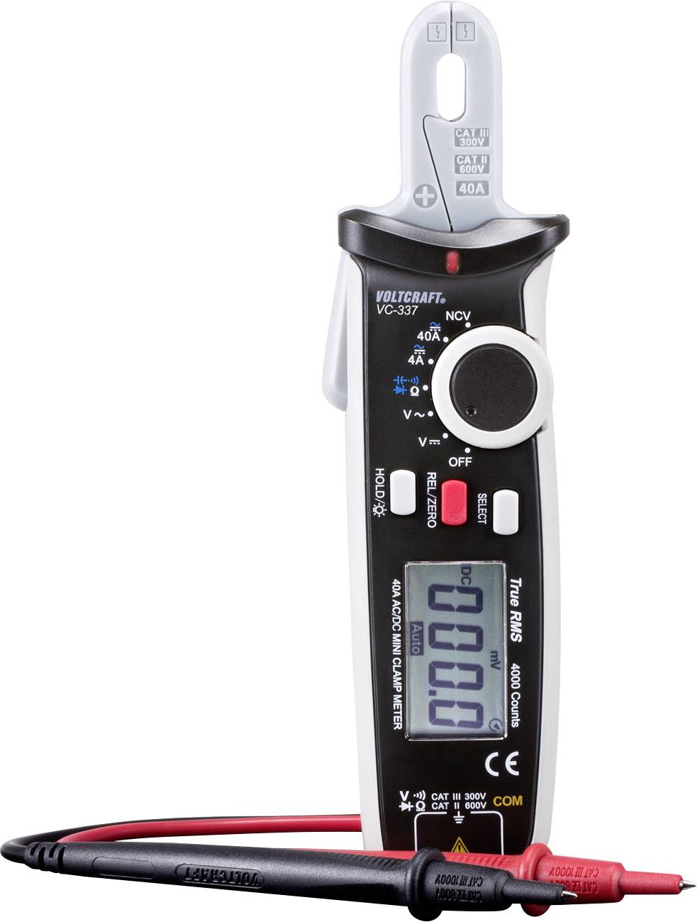
TRMS current clamps VC-337, thanks to their size and shape, are ideal for measuring in dense installations of distribution boxes and cars. Find them in SOS electronic assortment.
If you have ever measured in a distribution box, for example, the leads to individual circuit breakers, you have probably encountered a similar situation – conventional clamp multimeters have pliers that are too wide, and thus it is very difficult or even impossible to measure the current flowing through individual conductors close to the circuit breakers.
Clamp multimeters with an extra narrow shape of pliers, to which the Voltcraft VC-337 also belongs, elegantly solve this problem.
Besides narrow jaws, the device is relatively small and narrow itself, so it fits your hand very well. The VC337 can also measure DC current at 1mA, making it an ideal instrument for measurement in conventional DC equipment as well as in automotive installations.
Maximum display reading is 3999, and the range selection is automatic. The VC337’s high price/performance ratio is enhanced by the fact that the instrument measures the true effective value (TRMS) of AC values.
VC-337 current clamps can be found in our stable stock portfolio.
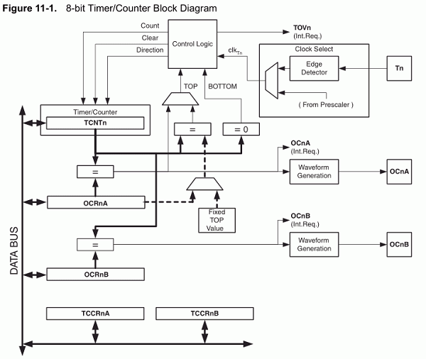
I’ve written a few software UARTs for AVR MCUs. All of them have bit-banged the output, using cycle-counted assembler busy loops to time the output of each bit. The code requires interrupts to be disabled to ensure accurate timing between bits. This makes it impossible to receive data at the same time as it is being transmitted, and therefore the bit-banged implementations have been half-duplex. By using the waveform generator of the timer/counter in many AVR MCUs, I’ve found a way to implement a full-duplex UART, which can simultaneously send and receive at up to 115kbps when the MCU is clocked at 8Mhz.
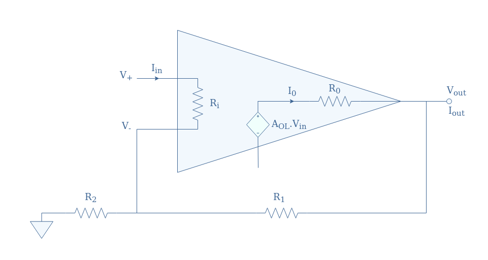
The voltage signal applied to an op-amp can either be supplied to its non-inverting input (+) or the inverting input (-). These different configurations are simply known as a non-inverting op-amp, and inverting op-amp. In this tutorial, we focus on the non-inverting configuration and present its details.
An overview of the non-inverting op-amp will be given in the first section through the concept of the ideal amplifier.
In the second section, real non-inverting configurations are discussed, we demonstrate the equations describing the gain and the input/output impedances.
Finally, examples of circuits based on the non-inverting configurations are given in the last section.
Ideal non-inverting op-amp
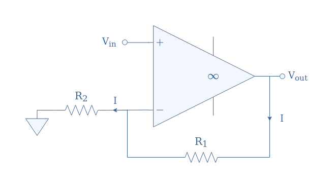
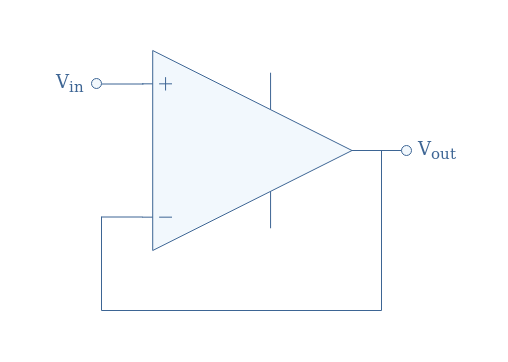
The goal of this section is to properly demonstrate and explain the ideal characteristics of the non-inverting configuration such as its input/output impedance and gain. The circuit representation of an ideal non-inverting op-amp is given in Figure 1 below.
Note that the symbol “∞” highlights the fact that the op-amp is here to be considered ideal. We highly recommend the reader to refer to the tutorial Op-amp basics for this section.
fig 1: Ideal non-inverting op-amp circuit
In this ideal model, the input impedance defined by the contribution of the resistance linking the inverting and non-inverting inputs (Ri in Figure 3) and the resistors R1 and R2, is infinite. Moreover, for an ideal circuit, Ri is supposed to be infinite, as a consequence, no currents can enter the op-amp through any input because of the presence of an open circuit.
This observation can also be summarized by saying that the node interconnecting the inverting input and resistances R1 and R2 is a virtual short. For this same reason, all the feedback current across R1 (I) is also found across R2.
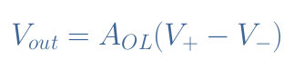
For the ideal model, the equality V+=V–=Vin is assured by the fact that the differential signal V+-V– can only be equal to 0 in order to produce a finite output Vout when multiplied by an infinite open-loop gain.
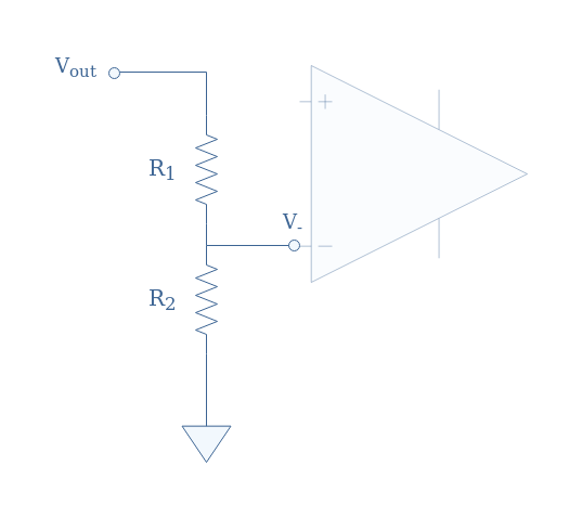
We can see the branches connected to the inverting input acting as a voltage divider circuit:
fig 2: Inverting branches seen as a voltage divider circuit
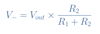
According to the voltage divider formula, we can express the inverting voltage V– as a function of the output voltage and the resistances:
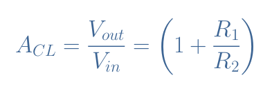
Since V–=Vin, after some simplification, we prove the expression of the gain in closed-loop ACL of an ideal non-inverting configuration:
eq 2: Closed-loop gain of an ideal non-inverting op-amp
We can note that the ideal gain presented in Equation 2 is strictly positive and higher than 1, meaning that the output signal is amplified and in phase with the input signal.
Real non-inverting op-amp
In a real op-amp circuit, the input (Zin) and output (Zout) impedances are not idealized to be equal to respectively +∞ and 0 Ω. Instead, the input impedance has a high but finite value, the output impedance has a low but non-zero value.
The non-inverting configuration still remains the same as the one presented in Figure 1.
fig 3: Internal equivalent circuitry of a real op-amp
Note that Ri and Ro can be described to be respectively the input and output impedances of the op-amp without any feedback loop (open-loop configuration).
Closed-loop gain
For a non-inverting configuration, Equation 1 still applies for V– , moreover, we have V+=Vin. However, since a low current can flow from the non-inverting input to the inverting input, the voltages are not equal anymore: V+≠V–.
We also need to remind that the inputs V+ and V– are linked with the output through the open-loop gain formula:
eq 3: Open-loop gain formula
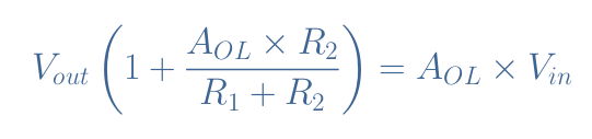
The equations for V+ and V– can be injected in Equation 3. After regrouping the terms “Vout” on one side of the equation and the terms “Vin” on the other, we get:
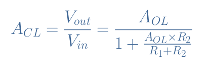
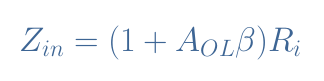
Finally, the closed-loop gain ACL for a real non-inverting configuration is given by Equation 4:
eq 4: Closed-loop gain of a real non-inverting configuration
For a real configuration, the gain not only depends on the resistor values but also on the open-loop gain
It is interesting to note that if we consider the op-amp to be ideal (AOL→+∞), the denominator is simplified to one term: AOLR2/(R1+R2). As a consequence, Equation 4 is simplified back to Equation 2.
Output impedance
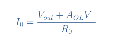
We start by assuming the equality of the currents across the resistances: IR1=IR2. Even if for real op-amps, a small leaking current enters the inverting input, it is several orders of magnitude smaller than the feedback current.
The current I0 across R0 (see Figure 3) can be expressed as a function of the voltage drop across R0 and the same value of the impedance R0:
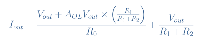
Since V– is described by Equation 1, the output current Iout can be expressed as the sum of I0 and the current flowing in the feedback branch given by Vout/(R1+R2):
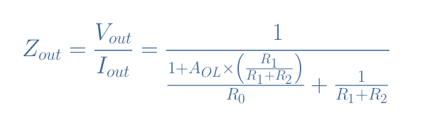
Finally, after rearranging the equation to obtain the ratio Zout=Vout/Iout, we can write the expression of the output impedance for a real non-inverting configuration:
eq 5: Expression of the output impedance for a real non-inverting configuration
We can note that in the case of an ideal op-amp, that is to say when AOL→+∞, we observe indeed Zout→0.
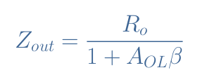
A simplified version for the expression of Zout is given by the following Equation 6:
eq 6: Simplified expression of the output impedance for a real non-inverting configuration
The term β is known as the feedback factor and is given by the ratio R1/(R1+R2). With that simplified version, we can still see that Zout→0 for an ideal op-amp situation.
Input impedance
The input impedance of a non-inverting configuration can be defined by the ratio V+/Iin (see Figure 3). For the input loop, we can write Kirchoff’s voltage law such as V+-Vin+IR2R2=0 with IR2 being the current across the resistor R2.
It can be shown that the expression of the input impedance can also be written as a function of the feedback factor:
eq 7: Expression of the input impedance for a real non-inverting configuration
Again, when the ideal situation is satisfied (AOL→+∞) we find that Zin→+∞ such as specified in the first section.
Non-inverting op-amp examples
Buffer circuits
The most simple designs for non-inverting configurations are buffers, which have been described in the previous tutorial Op-amp Building Blocks. In this configuration, R1=0 and R2→+∞ as we can present in Figure 4 below:
fig 4: The buffer circuit
This buffer (or voltage follower) has a unity gain and does not invert the output, meaning that Vout=Vin. Its high input impedance and low output impedance are very useful to establish a load match between circuits and make the buffer to act as an ideal voltage source.
Example
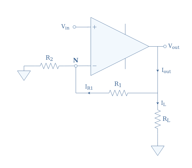
We consider a real non-inverting configuration circuit given in Figure5:
fig 5: Example of real non-inverting configuration
The resistors, input value, and gain in open-loop are given such as:
R1=10 kΩ
R2=2 kΩ
RL=1 kΩ
Vin=1 V
AOL=105
First of all, we can compute the value of the closed-loop gain ACL. By using Equation 4 we obtain ACL=5.99 while Equation 2 gives ACL=6. We can remark that both values are very similar since AOL is high. Typical values of AOL for real op-amps range between 2×10⁴and 2×10⁵, which is high enough to always consider Equation 2 valid.
From this value, we can simply say that the output voltage is given by Vout=ACL×Vin= 6 V.
The currents IR1 (across R1) and IR2 (across R2) are approximately equal if we consider the leaking current in the inverting input to be much lower than the feedback current. Due to the virtual short existing at the node N, VN=Vin, and therefore we have IR1=IR2=Vin/R2=0.5 mA.
Since the current IL through the output load is given by Vout/RL=6 mA, we can determine the output current thanks to Kirchoff’s current law: Iout=IL+IR1=6.5 mA.
Finally, we can also specify the output impedance to be Zout=Vout/Iout=920 Ω.
Conclusion
When the input signal is supplied to the pin “+”, the op-amp is said to be in a non-inverting configuration. The design and main properties of this configuration are presented in the first section that presents its ideal model.
In the second section, the real non-inverting op-amps are presented. Due to the parasitic phenomena that are intrinsic to their design, their properties change, the expression of the closed-loop gain, input, and output impedances are different. However, the simplified version of these formulas that describe the ideal model can indeed be recovered when we set the open-loop gain to be infinite.
Examples of real configurations are shown in the last section, we present how to calculate the main characteristics of a configuration with the knowledge of the resistors value and input voltage.
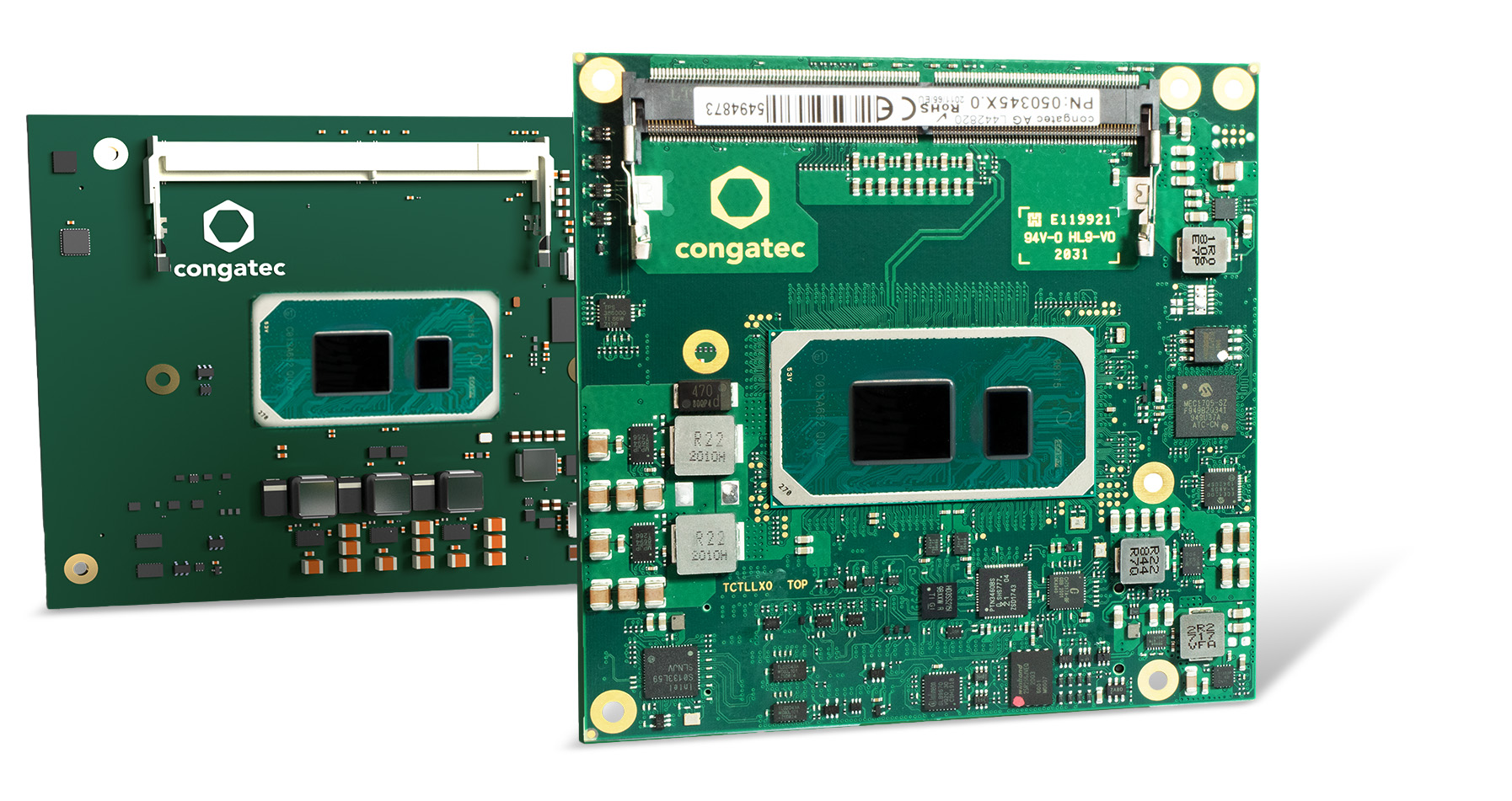
congatec fuels launch of 11th Gen Intel® Core™ processors with two great new design options
In parallel with the 11th Gen Intel® Core™ processor launch (code named “Tiger Lake”), congatec – a leading vendor of embedded computing technology – announces the availability of both its first COM-HPC Client size A module and a next generation COM Express Compact Computer-on-Module. This provides engineers the choice to further scale the performance of their existing systems or develop the next generation of products utilizing COM-HPC’s broader array of interfaces. OEMs will benefit from the substantial performance improvements as well as communication enhancements that the new modules based on 11th Gen Intel Core processors deliver to the high-end computing sector. Typical applications can be found in many high-end solutions, from embedded systems and edge computing nodes to network hubs, and local fog data centers to core network appliances, as well as ruggedized central cloud data centers for critical government applications.
“congatec’s modules based on the 11th Gen Intel Core processors feature high-performance CPU/GPU compute with integrated AI acceleration for critical applications that demand high-speed processing, and computer vision,” explains Gerhard Edi, CTO at congatec. The highlights of the 11th Gen Intel Core processors provide a massive CPU performance boost, fast DDR4 memory, expansive PCIe Gen4 and USB 4.0 bandwidth. These performance enhancements are complemented by features that are critical for communication connected edge computers such as congatec’s support for hypervisor technologies e.g. from Real-Time Systems. All this comes in a powerful and energy-efficient package leveraging Intel’s SuperFin technology delivering increased power savings, physical density and providing even more compute power for given thermal envelopes.
The benefits of choice
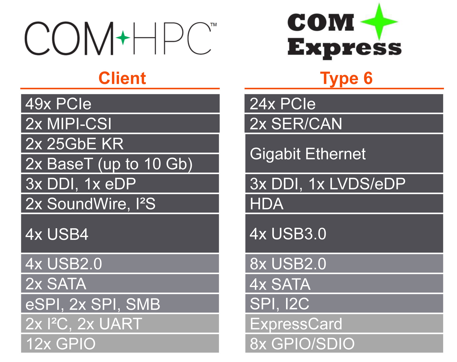
“For the first time, design engineers now have the choice to go either with COM Express or COM-HPC. Each provide unique benefits for example, we have an improved next-gen connector for COM Express that is expected to offer better bandwidth capacities compared to what was available in the past. This is essential information for engineers thinking about utilizing the high bandwidth interfaces such as PCIe Gen 4. Engineers choosing COM-HPC will benefit from by far more high-speed interfaces delivered over 800 signal pins in total. This is almost twice as many pins as COM Express Type 6 modules deliver with 440 pins,” explains Andreas Bergbauer, Product Line Manager at congatec.
To help engineers make the best choice, congatec provides engineering support and is creating a COM Express and COM-HPC design decision guide and a whitepaper, which will be available on congatec’s 11th Gen Intel Core processors page.
Even more innovations and benefits
It is important to mention that besides PCIe Gen 4, the new congatec Computer-on-Modules with low-power 11th Gen Intel Core processors also offer USB 4.0, which is fundamentally based on Intel’s Thunderbolt technology. USB 4.0 supports amazing data transfer rates of up to 40 Gbit/s and tunneling of PCIe 4.0 as well as DP-Alt mode supporting video signals of up to 8k resolution with 10-bit HDR at 60 Hz.
The feature set in detail
The COM-HPC Client size A module conga-HPC/cTLU as well as the COM Express Compact conga-TC570 will become available with the 11th Gen Intel Core processors. Both modules are the first to support PCIe x4 in Gen 4 quality to connect external peripherals with massive bandwidth. In addition, designers can leverage 8x PCIe Gen 3.0 x1 lanes. Where the COM-HPC module offers latest 2x USB 4.0 and 2x USB 3.2 Gen 2 and 8x USB 2.0, the COM Express module offers 4x USB 3.2 Gen 2 and 8x USB 2.0 in compliance to the PICMG specification. Sound is provided via I2S, SoundWire by COM-HPC, and HDA by COM Express modules. Comprehensive board support packages are provided for all leading OS’s like Linux, Windows and Chrome, as well as hypervisor support from Real‑Time Systems.
Further information about congatec’s new modules based on 11th Gen Intel Core processors can be found on the main landing page www.congatec.com/11th-gen-intel-core/
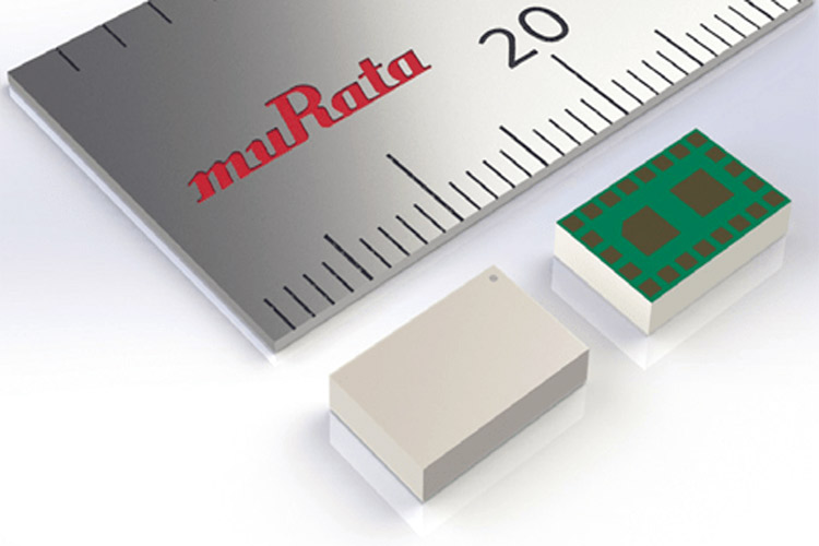
Murata Electronics today announced the availability of the Type 1RM ultra-small Medical Implant Communication System (MICS) band radio module. The LBAA0PC1RMH298 is designed for use in devices with data-intensive wireless capabilities that are used to diagnose, monitor, report, and provide warnings in support of human life. Typical applications include insulin, drug, and baclofen pumps as well as arrhythmia and bladder monitors.
Measuring just 8.6 x 5.6 x 1.7mm, this module is one of the smallest and most highly integrated solutions available. What differentiates the LBAA0PC1RMH298 from alternative products is Murata’s proprietary technique that discretely bundles several technological components and ICs into one miniatured package. The result is an advanced module that delivers a communication range up to two meters, an ultra-low current consumption of 0.2uA Sleep State, and a 128 kbps data rate.
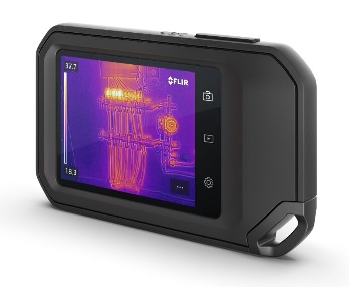
Flir C5 brings all the best from older C3 but features several major improvements. The main are 4x higher IR resolution (160x120px) and the WiFi + Bluetooth connectivity. Simply put, the ideal thermal camera for the fieldwork.
If you liked the popular pocket-sized industrial thermal cameras Flir C2 and C3 Series, you would certainly love the new C5.
Main features:
4x higher IR resolution (160x120px) comparing to C3 model
Instant backup of your images to Flir Image Cloud Ignite (FREE 1 GB Storage, software available on PC and mobile).
Automatic or Manual setting of level and span of temperatures of your measuring object? All available at one click.
3,5” LCD screen (+36% more area in comparison to C3)
5MPx visual camera
Double the operating battery life up to 4 hrs
Possibility to input notes and edit in the gallery, directly in the camera
Built-in tripod mount
IP rating 54
Measuring range -20 to +400°C
Naturally, even the Flir C5 features MSX function for overlaying images in an infrared and visible spectrum for easier identification.
It’s worth saying that in contrast with some cheaper types of infrared cameras on the market, stored images are fully thermometric, i.e. the stored image file carries information about the temperature of every pixel measured with IR camera with the possibility to post-process in Flir tools SW.
With Flir C5, you can edit images and use the Cloud feature to create and share reports directly from the measurement point much faster and easier. In many cases, you do not have to sit by the computer, but create a report from the measurement directly in the field.
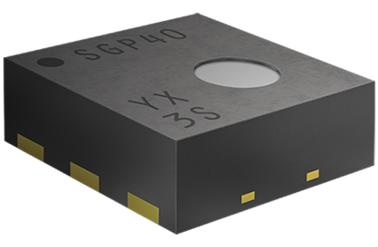
Sensirion has introduced a new SGP40 VOC (Volatile Organic Compound) sensor for maintaining indoor air quality in modern buildings. VOCs are the most responsible components for bad air quality in the modern buildings, this needs to be monitored and necessary steps should be taken to maintain the air quality. The new broadband VOC, SGP40 can identify VOC pollution source and allows the user to take necessary action when they are built into an air quality monitor.
With an integrated CMOSens sensor system on a single chip based on a metal oxide sensor provides a humidity compensated indoor air quality signal via a digital I2C interface. With outstanding long term stability of sensing and response time, the SGP40 provides low power consumption for battery-driven applications.
The VOC algorithm analyses the VOC events from the SGP40 and store them in a VOC index that qualifies the VOC events relative to each sensor’s average indoor environment. The VOC index states that to what extent the indoor air quality has deteriorated or improved to the average VOC environment, using this data users can gradually control the fan of an air treatment device or they can use it as feedback on their daily activity profile. Both SGP40 and the evaluation kit are available through the Sensirion’s distribution network.