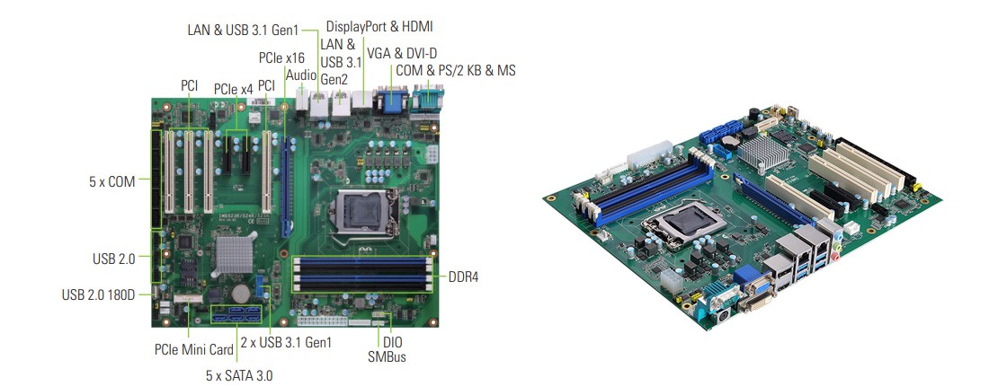
Axiomtek – a world-renowned leader relentlessly devoted in the research, development and manufacture of series of innovative and reliable industrial computer products of high efficiency – is pleased to announce the IMB525R, its new server-grade ATX motherboard powered by the Intel® Xeon® E, 9th/8th generation Intel® Core™, Intel® Pentium® or Intel® Celeron® processors with the Intel® C246 chipset. The ATX motherboard offers optimum processor performance, unparalleled flexibility, rich I/O expandability and superior graphics performance; additionally, the server-grade platform supports Error-Correcting Code (ECC) memory which provides improved data integrity and system reliability through automatic data correction. It also features five SATA-600 ports with software RAID 0/1/5/10 for reliable data storage and protection. The IMB525R is specifically suited for industrial workstations, embedded networks, factory automation, robotic motion control, machine vision, and testing and measurement.
“Powered by Intel® C246 chipset, Axiomtek’s IMB525R supports the latest Intel® Xeon® E processor and 9th generation Intel® Core™ processor and has four 288-pin DDR4-2666/2400 ECC DIMM slots with a maximum memory capacity of 128GB. In addition, the IMB525R offers flexible expandability with one PCIe x16 slot, two PCIe x4 slots, four PCI slots and one PCI Express Mini Card slot to meet customer-specific needs,” said Brandon Wang, the product manager of IPC Division at Axiomtek. “The IMB525R supports Trusted Platform Module 2.0 (TPM 2.0) to enhance network security whether as a cloud server, data center, or for IIoT applications. This Intel® Coffee Lake Refresh-based ATX motherboard is designed to reduce overall development cost and speed up time-to-market.”
The IMB525R is integrated with the Intel® UHD Graphics 630 for superb visual performance, enabling triple simultaneous displays via DisplayPort++, HDMI, DVI-D, and VGA for multi-display applications. The IMB525R comes with two USB 3.1 Gen 2 ports, four USB 3.1 Gen 1 ports and seven 180D type A USB 2.0 ports for ultimate connection flexibility. It has four RS-232, two RS-232/422/485, two Gigabit LANs with Intel® Ethernet controller I211-AT and Intel® Ethernet connection I219-LM, eight-channel digital I/O, one HD Codec audio, one SMBus, and one PS/2 keyboard and mouse. Furthermore, it can operate under a wide temperature range from 0°C to +60°C for use in harsh environments. More features include watchdog timer and hardware monitoring functions.
Advanced Features:
LGA1151 socket 9th/8th generation Intel® Core™ i7/i5/i3, Intel® Xeon® E, Intel® Pentium® or Intel® Celeron® processor (code name: Coffee Lake Refresh)
Intel® C246 chipset
Four 288-pin DDR4-2666/2400 ECC DIMM for up to 128GB of memory
Supports DisplayPort++, DVI-D, HDMI and VGA with three independent display outputs
Five SATA-600 with RAID 0/1/5/10 function
Supports one PCI Express Mini Card slot
Supports two USB 3.1 Gen2 and four USB 3.1 Gen1 ports
TPM 2.0 (optional)
Axiomtek’s new IMB525R is now available for purchase. For more product information or pricing, please visit our global website at www.axiomtek.com or contact one of our sales representatives at info@axiomtek.com.tw.
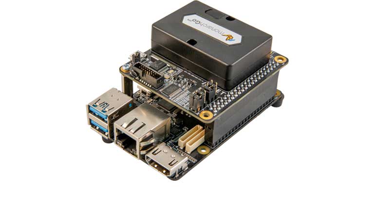
The Monarch Go Pi HAT enables engineers to connect Raspberry Pi HAT-capable SBCs to the Monarch Go LTE Cat-M1 modem. The Monarch Go Pi HAT supports both the Monarch Go and Monarch Go-GPS modems. In addition to Monarch Go support, the Pi HAT includes a shuttle click expansion connector that enables 3.3V I/O I2C, SPI, UART, and GPIO-based click modules from MikroElektronika. Having access to the large array of click module offerings permits prototyping of various LTE-based applications.
The Monarch Go Pi HAT can operate in two modes. The first mode works with a SBC over a Pi HAT 40-pin GPIO UART interface. In this mode, the SBC performs the communication over the UART interface with the Monarch Go modem. The second operating mode for the Monarch Go Pi HAT is standalone. In standalone operation, the Monarch Go Pi HAT’s power and UART communication to the modem occur through the micro USB interface. In standalone operation, it functions like the Monarch Go Starter Kit and can be evaluated on many other platforms over the USB-UART interface.
Features
Raspberry Pi HAT Compatible
Monarch Go LTE modem
Cat-M1
Pre-installed Verizon ThingsSpace IoT SIM
Production ready
MikroElektronika shuttle click site
3.3V I/O
I2C
SPI
GPIO
UART
Voltage I/O translator
1.8V to 3.3V
Micro USB
Debug and Programming UART
The Monarch Go LTE Cat-M1 modem delivers the shortest possible route to market and lowest development cost for cellular IoT connected devices. Unlike traditional cellular modules, this modem is certified for use on the Verizon network, which avoids costly lab testing while improving time to market. The Monarch Go has an integrated antenna and pre-installed Verizon ThingSpace IoT SIM card, giving developers an easy, cost-effective approach to developing LTE IoT solutions.
The Monarch Go Pi HAT kit is available in the Americas for USD $72.95. Learn more about this product. Raspberry Pi products and accessories, including the new Raspberry Pi 4 Model B computer with 8GB of onboard memory, are available from Newark, an Avnet Company.
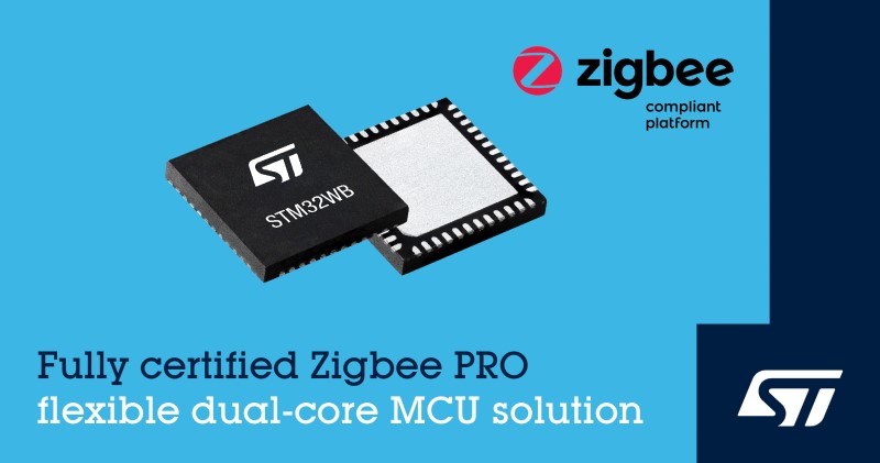
STM32WB55 microcontrollers also support Thread and Bluetooth 5.0 with Flash Memory up to 1Mb
STMicroelectronics STM32WB55 Wireless Microcontrollers now incorporate Zigbee® 3.0, based on Zigbee PRO protocol stack support, enabling STM32 developers to leverage the interoperability and power-saving features of Zigbee networking for projects such as home automation, smart-lighting, smart-building, and broader IoT connectivity.
Zigbee 3.0 unifies the features of Zigbee specifications for both consumer and industrial applications, a move that has driven major consumer and Internet brands to choose Zigbee connectivity for smart-home products. A long-term supporter of Zigbee technology, ST is a member of the Zigbee Alliance board of directors, a council member of the Zigbee Alliance Member Group China (ZMGC), and supportive of the Zigbee Alliance Connected Home over IP (CHIP) project.
ST’s Zigbee 3.0 software for STM32WB55 includes the highly regarded Exegin Zigbee PRO protocol stack, provided free of charge, and delivered and fully supported by ST. This stack is used in Exegin products certified as Zigbee Golden Units and is approved as a reference stack for use by test laboratories. To further assist development, ST’s offer supports 46 Zigbee 3.0 clusters that help users quickly establish device capabilities. A further 21 clusters support legacy products.
Leslie Mulder, Exegin’s President said;
“This is a milestone for the Zigbee Alliance, with the advent of ST’s Zigbee 3.0 offering, Zigbee is reaching a new level of maturity, one that has the potential to cement its and ST’s leadership roles in the IoT market.”
STM32WB55 microcontrollers also support Thread and Bluetooth 5.0, with over-the-air update (OTA) capability. There are currently 10 STM32WB55 variants, offering a choice of package styles and Flash density from 256Kbyte to 1Mbyte. Further variants scheduled to be introduced in the next quarter will give developers extra flexibility to meet application performance and cost targets. The devices feature the Arm® Cortex®-M4 with Floating Point Unit, DSP instructions, and a memory protection unit (MPU) that enhances application security. Arm® Cortex®-M0+ coprocessor dedicated to managing the integrated IEEE 805.15.4 radio and the MCU’s cyber-protection features ensures real-time low-layer operations run smoothly without compromising application execution. The RF transceiver has a link budget of 106dB, to ensure reliable connections over distance.
ST’s patented ultra-low-power microcontroller technologies and high feature integration, which include the radio balun circuitry, ensure STM32WB55 devices help designers meet tight power and size constraints in a wide range of IoT and wearable devices. There are rich analog and system peripherals, as well as cyber-protection and ID features including secure firmware installation (SFI), customer key storage, hardware public key authority (PKA), and cryptographic accelerators. Capacitive touch and LCD controllers also simplify user-interface integration.
The Zigbee 3.0 software is now included in the STM32CubeWB MCU Package, which provides embedded software including low-layer (LL) APIs and hardware-abstraction layer (HAL) drivers for STM32WB microcontrollers, as well as Bluetooth® 5.0, Mesh V1.0, and Thread® libraries, FreeRTOS™ kernel, FatFS file system, and the STMTouch™ capacitive-sensing library. The STM32Cube ecosystem, through STM32CubeMonitor-RF for RF testing and STM32CubeMX for device configuration and code generation, ensures more comfortable and easy development.
Features of the STM32WB55RG dual core Arm Cortex-M4, Cortex-M0+ Microcontroller include
Core
Arm® 32-bit Cortex®-M4 CPU with FPU, frequency up to 64 MHz, MPU, 80 DMIPS and DSP instructions
Dedicated Arm® 32-bit Cortex® M0 + CPU for real-time Radio layer
Radio
2.4 GHz
RF transceiver supporting Bluetooth® 5 specification, IEEE 802.15.4-2011 PHY and MAC, supporting Thread and Zigbee® 3.0
RX sensitivity: -96 dBm (Bluetooth® Low Energy at 1 Mbps), -100 dBm (802.15.4)
Programmable output power up to +6 dBm with 1 dB steps
Integrated balun to reduce BOM
Support for 2 Mbps
Accurate RSSI to enable power control
Suitable for systems requiring compliance with radio frequency regulations ETSI EN 300 328, EN 300 440, FCC CFR47 Part 15 and ARIB STD-T66
Support for external PA
Available integrated passive device (IPD) companion chip for optimized matching solution (MLPF-WB55-01E3 or MLPF-WB55-02E3)
Memories
Up to 1 MB Flash memory with sector protection (PCROP) against R/W operations, enabling authentic Bluetooth® Low Energy and 802.15.4 SW stack
Up to 256 KB SRAM, including 64 KB with hardware parity check
20×32-bit backup register
Boot loader supporting USART, SPI, I²C and USB interfaces
OTA (over the air) Bluetooth® Low Energy and 802.15.4 update
Quad SPI memory interface with XIP
Performance benchmark
1.25 DMIPS/MHz (Drystone 2.1)
219.48 CoreMark® (3.43 CoreMark/MHz at 64 MHz)
Energy benchmark
303 ULPMark™ CP score
Ultra-low-power platform
1.71 to 3.6 V power supply
– 40 °C to 85 / 105 °C temperature ranges
13 nA shutdown mode
600 nA Standby mode + RTC + 32 KB RAM
2.1 µA Stop mode + RTC + 256 KB RAM
Active-mode MCU: < 53 µA / MHz when RF and SMPS on
Radio: Rx 4.5 mA / Tx at 0 dBm 5.2 mA
Supply and reset management
High efficiency embedded SMPSstep-down converter with intelligent bypass mode
Ultra-safe, low-power BOR (brownout reset) with five selectable thresholds
Ultra-low-power POR/PDR
Programmable voltage detector (PVD)
VBAT mode with RTC and backup registers
Clock sources
32 MHz crystal oscillator with integrated trimming capacitors (Radio and CPU clock)
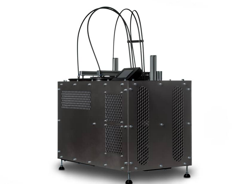
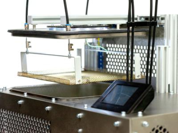
A new crowd supply campaign has been launched for the Vapor Phase One, which is the industry’s most dynamic PCB soldering method available now to hobbyists and development engineers alike. Compared to infrared and conventional soldering, the vapor phase process works perfectly at controlling high thermal mass assemblies. Big SMD capacitors, high-power inductors, also metal substrate PCBs are no match for the Vapor Phase One, that are capable of soldering fine pitch structures and heat reactive components without risk of damage, also its analogous temperature distribution reduces warp and bow of the PCB, that reduces internal stresses on the assembly. Vapor Phase One depends on two integrated lifts to enable results similar to those you would get using an industrial production. The Vapor Phase One helps you improve your way of soldering, and guarantees less risk of cold-solder joints, PCB tombstoning, and solder bridges.
Vapor-phase soldering is also called condensation soldering and it depends on physics which is like those that drives a heat pipe. An inert liquid is used which is slightly above its boiling point, and it leads to a vapor phase being formed just over the surface. (For Vapor Phase One, the liquid is specially made and it’s known as Galden ® the medium boils between 230°C and 240°C). This newly made vapor moves energy from the heat source to one or more “heat sinks”. Those heat sinks are the PCB, the components, and the solder paste you have to use for application between them. Vapor condenses on a cooler surface first, so that it can transport a large amount of energy to those areas, slowly heating up your assembly. The solder paste will then melt as your PCB gets to its appropriate temperature, which depends on the solder paste which is mostly 180°C. Also, the maximum temperature it can reach is limited by the boiling point of the Galden. As soon as you remove your assembly from Vapor Phase One, the solder will solidify.
Features Of Vapor Phase:
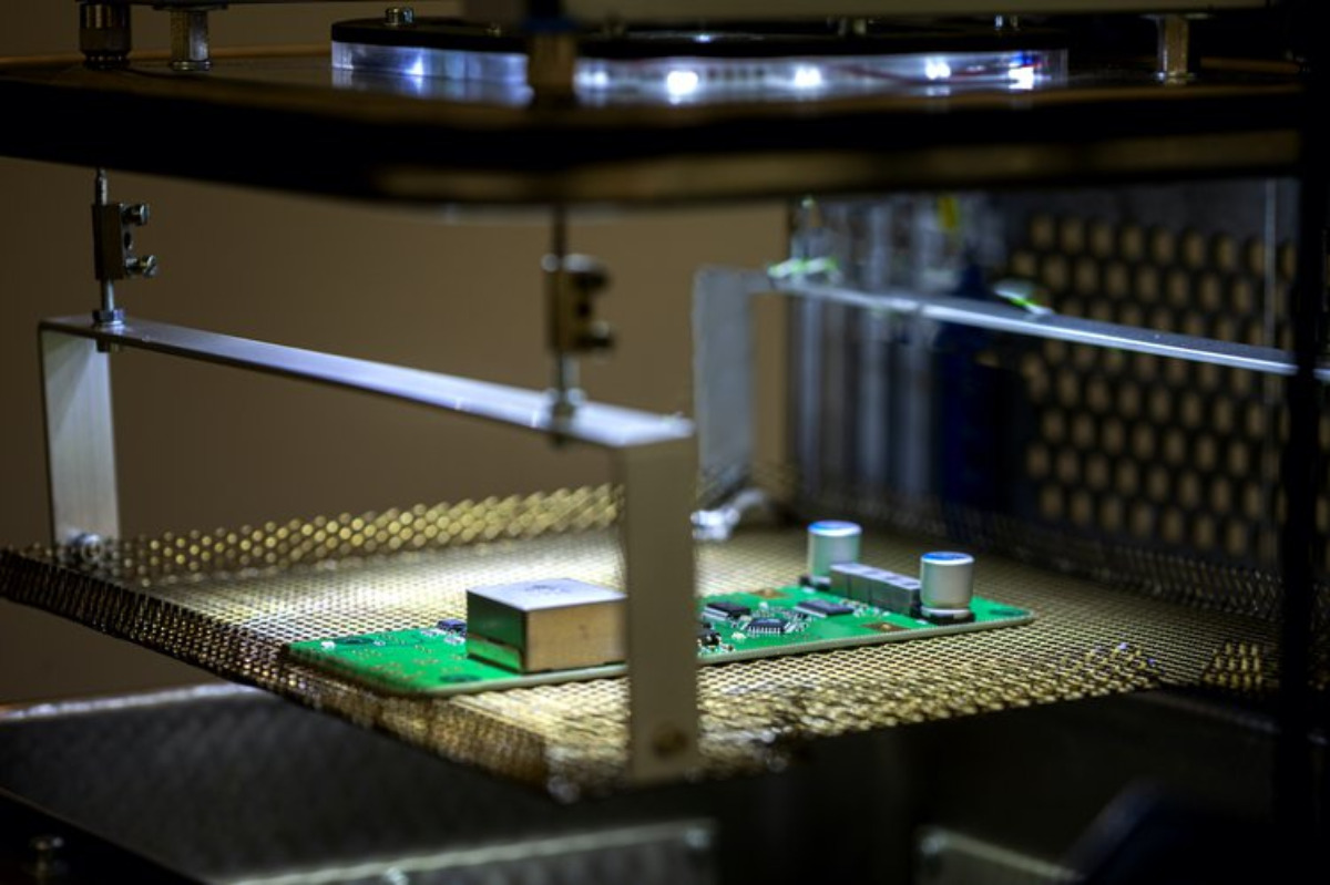
Fast temperature profile: The way the VP One is designed, enables the handler to run fast temperature profiles by using a height-adjustable PCB carrier. The assembly is placed on an open wire mesh, some distance above the heat-transfer medium, as determined by a fast temperature control loop.
Individual Soldering Profiles: VP One can import soldering profiles via a USB interface where they are stored as CSV formatted data. It makes use of these profiles to adjust heating-power, and lift position to account for different solder pastes and PCB technologies. You don’t need an external control software.
Conservation of heat-transfer medium: There is a quick cool feature that enables the entire capacity of Vapor Phase One’s cooling circuit, plus four additional fans mounted to its base, to be used to cool the process chamber as quickly as possible after a soldering process. This optional “Quick Cool” feature reduces the process time and ensures a minimum loss of Galden when the board is removed.
Lid lift : The lid to the process chamber lifts automatically to enable the injecting and ejecting of a PCB. This safety feature also contributes to the preservation of heat-transfer medium.
Viewing window: In addition to a screen that displays realtime temperature data, Vapor Phase One features a viewing window, complete with internal lighting, that enables you to see inside the process chamber.
Specifications:
Usable heat-transfer media: 230, XS 235, and HS 240
Volume of Galden : 500 to 1000ml (cost $170 to $340)
Cooling : Water and air
Dimensions: 50 x 46.5 x 32cm
Max. Power consumption: 1.1 kW(at 230V or 110V)
Maximum PCB size: 20 x 18.5 x 7 cm
Weight: 18 kg
Max. power consumption: 1.1 kW (at 230 V or 110 V)
Data interface: USB or SD card
Touchscreen: 4-inch display with 800 x 480 pixels
Vapor Phase One is an open hardware driven by open-source firmware,
“and we intend to publish everything that goes into building one. That includes a bill of materials, schematics, Gerbers, and step files, along with GPL-licensed firmware. You can already find much of this in our GitHub repository, but we will continue adding and updating source code and design files throughout the campaign. As soon as crowdfunding is complete, we will prepare for small-scale production of Vapor Phase One machines and begin pursuing CE and any other relevant certifications.”
Funding ends on Sep 08, 2020 at 04:59 PM PDT (11:59 PM UTC).
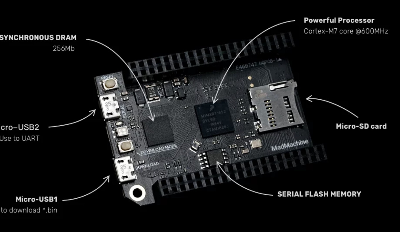
One growing trend across the embedded systems development world is the development of boards, Microcontrollers, and general development platforms, that aim to be more inclusive, with respect to supporting other programming languages asides the traditional C/C++ that are synonymous with embedded development. From boards like the Espruino which supports Javascripts out of the box, these boards reduce the embedded system barrier of entry in a way that allows developers from other backgrounds like Software to quickly get up and running on hardware projects. With a lot of ground a language still to cover, a new board, developed by the folks at MadMachine, is taking things further with support for Swift; the programming language popular among iOS developers.
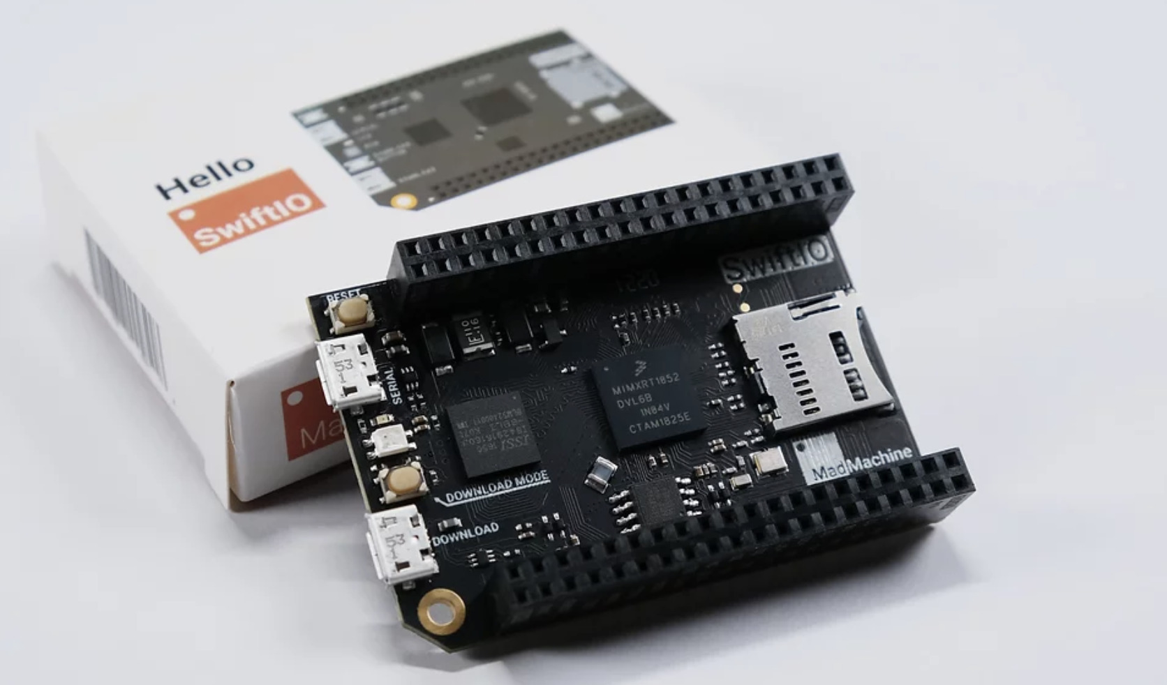
The new board called; the SwiftIO board, is a compact electronics development board that runs Swift on the bare metal, giving you a system that can be used for the development of all kinds of electronics. The design of the board took a cue from the ease and fun associated with the Arduino and it thus supports a range of sensors, lights, and motors that are plug-and-play compatible with Arduino boards.
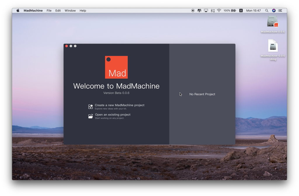
The new development board is accompanied by the MadMachine IDE which offers a full Swift compiler and framework environment that runs on the microcontroller making the development process easy. Despite being popular only among iOS developers, Swift is regarded as a modern general-purpose programming language that incorporates modern approaches to ensure safety, performance and support the implementation of a well-built software design patterns.
The modern and safety features of Swift as a programming language makes it perfect for the future of IoT development and MadMachine is hoping to provide designers with the tools required to leverage those features.
Some features of the SwiftIO board include:
i.MX RT1052 Crossover Processor with Arm® Cortex®-M7 core @600MHz
Micro SD card slot, supporting standard and high capacity SD cards
Micro USB connector for power
On-board USB to UART for serial communication
46 GPIO on left and right edges
On-board GRB LED
12x 12-bit analog to digital (ADC) converters
4 UART, 2 CAN, 2 IIC, and 2 SPI
14 PWM pins
Asides providing a platform for makers to build amazing solutions, MadMachine also hopes the SwiftIO development board will provide a cheap path for makers beginners and enthusiasts that are interested in learning the Swift programming language since the cost of the SwiftIO board is 80% lower than that of the cheapest Apple iPad.
The board is currently available for sale on MadMachine’s store for $68 and users have the option of picking up the SwiftIO maker kit containing different sensors and actuators alongside the SwiftIO board, for $118.
More information on the board, pricing, availability, and features, can be found on MadMachine’s Website.
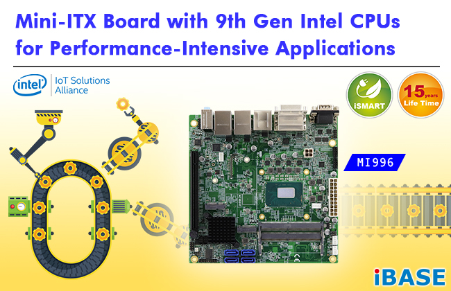
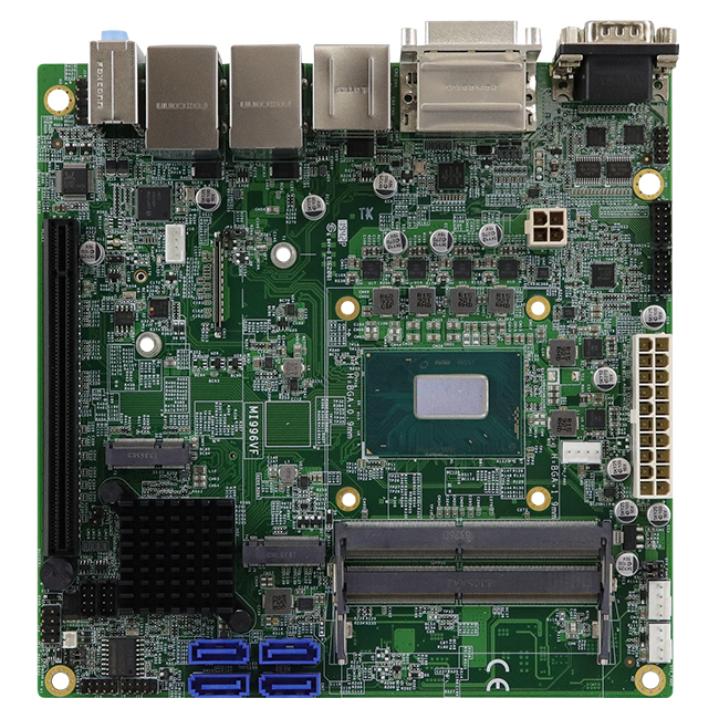
IBASE Technology Inc. (TPEx: 8050), a leading provider of industrial motherboards and rugged computing solutions, has launched the MI996 Mini-ITX motherboard that is powered by the latest 9th Gen Intel Xeon E and Core™ processors. Designed for a wide array of applications such as medical, industrial automation and kiosks, it supports integrated GPU and PCI-E x16 for a discrete graphics card to run simultaneous displays in four video outputs: eDP, HDMI (2.0a), Display Port and DVI-D.
The compact MI996 is suitable for space-constrained applications and packs powerful functionality into a compact Mini-ITX form factor (170mm x 170mm). Enhanced I/O connectivity and expansion comprises six USB 3.1, four USB 2.0, four serial ports, four 4x SATA III, a Mini PCI-E, as well as two M.2 slots for NVMe storage and CNVi WiFi or Bluetooth connections. It features two Gigabit LAN and up to 32GB of DDR4-2666 SO-DIMM memory (ECC and non-ECC) for high-performance computing.
Two model series of MI996 are available with the Intel CM246, QM370, and HM370 chipsets to support a range of Intel processors. Other advanced features include a watchdog timer, Digital I/O, iAMT (11.6) remote management, TPM (2.0) security, iSMART (3.8) green technology, and vPRO (MI996VF series). By consolidating superior performance, versatility and scalability, the MI996 enables system integrators to deliver a highly optimized embedded solution to their customers.
MI996 FEATURES:
Onboard 9th Gen Intel® Xeon® E / Core™ i7/i5/i3 / Celeron® processors
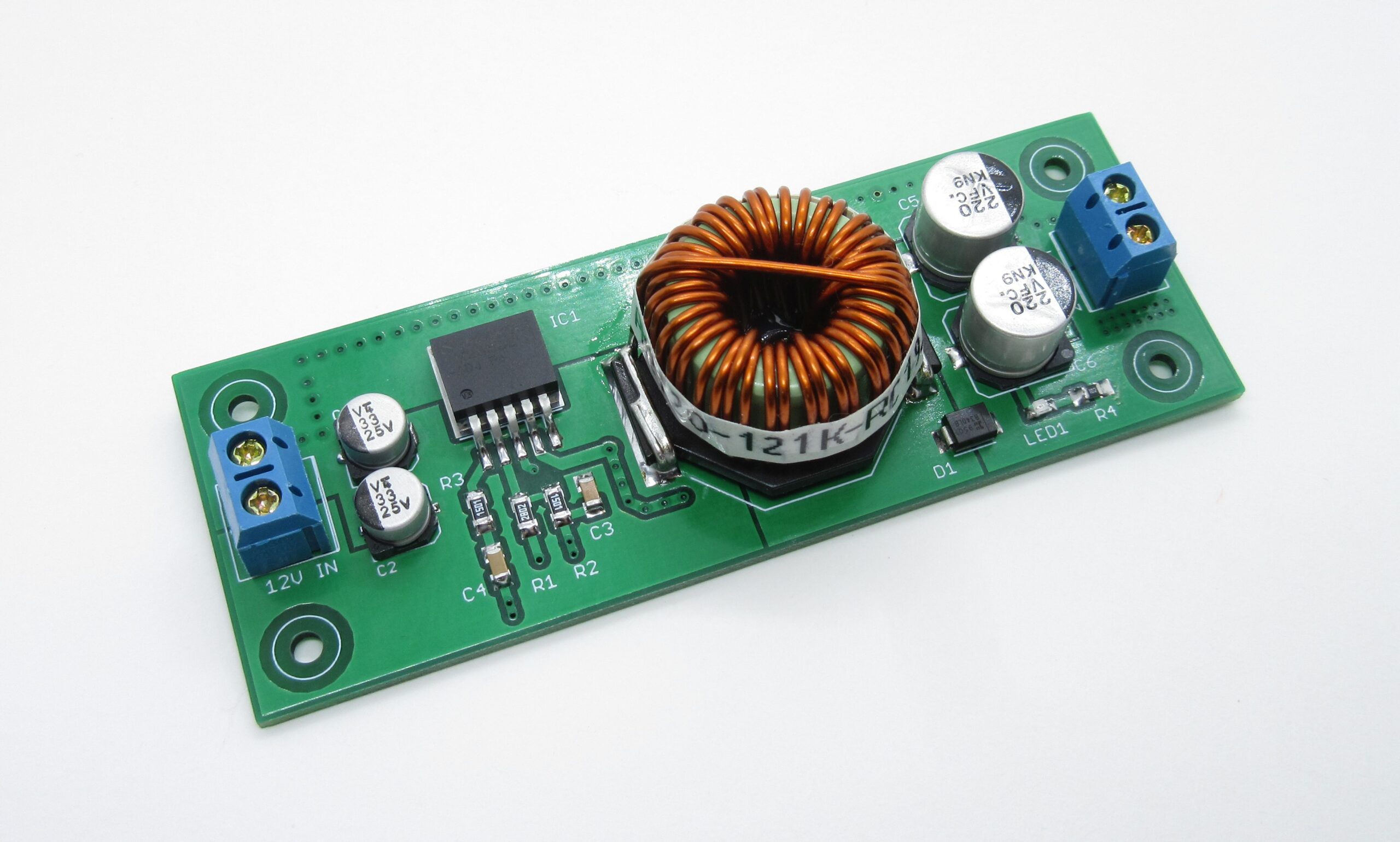
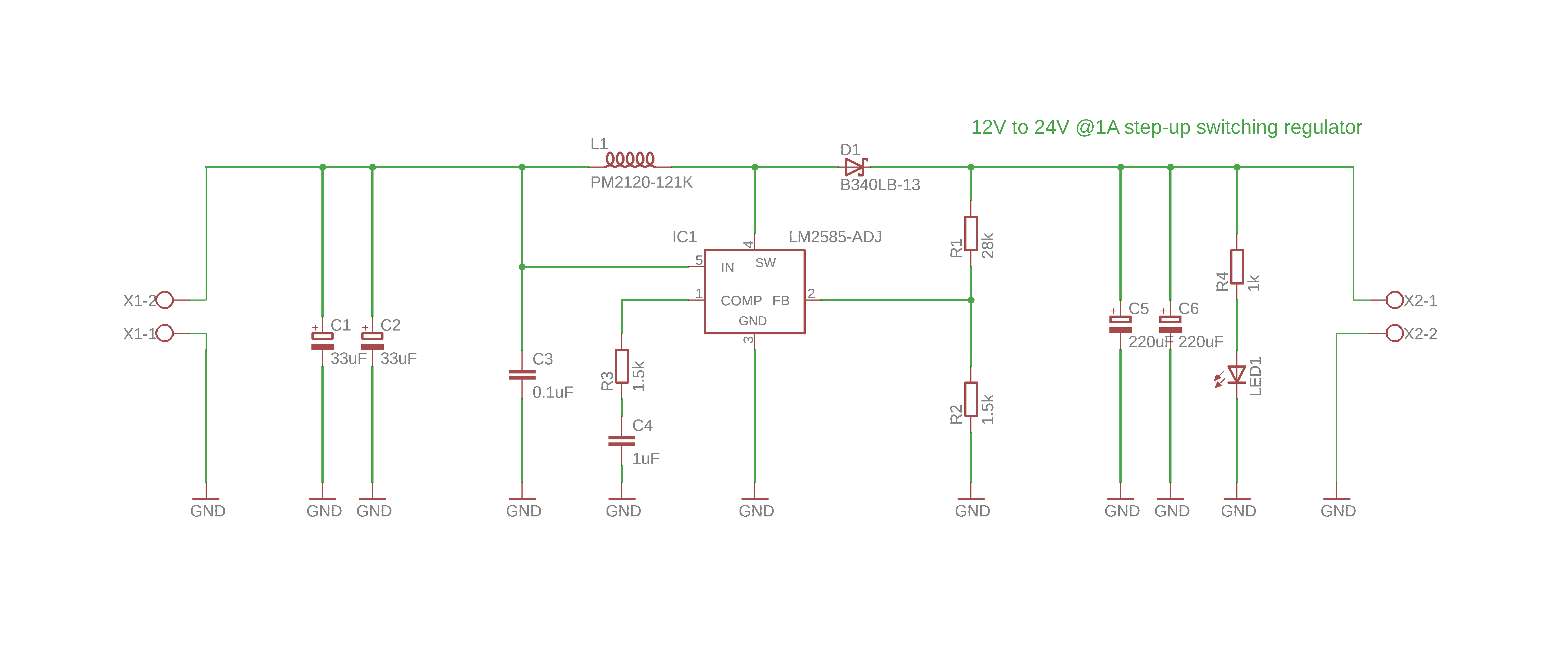
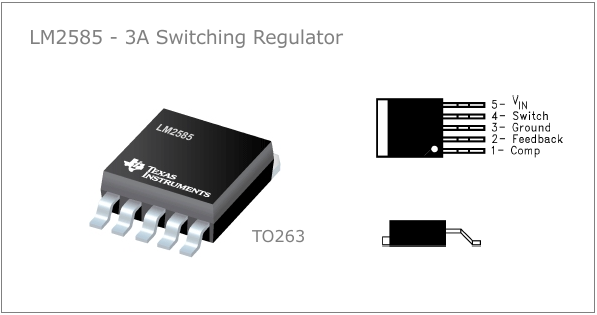
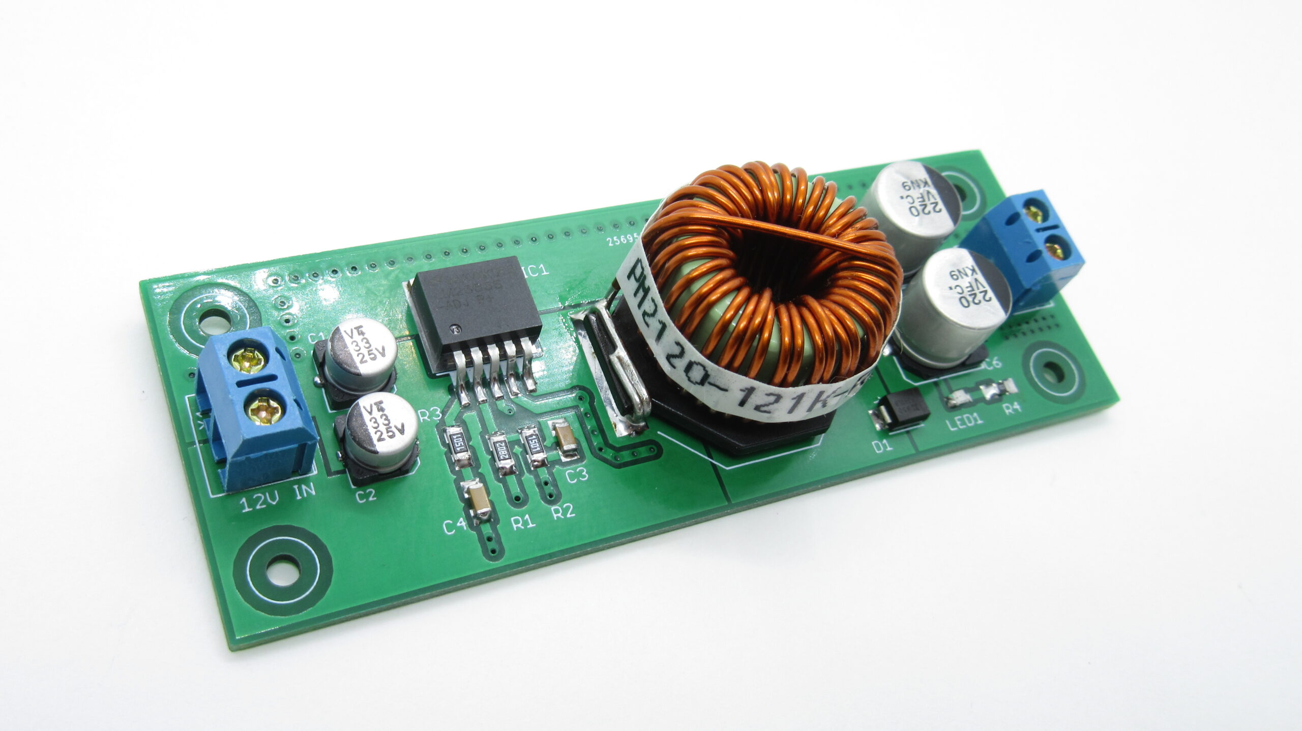
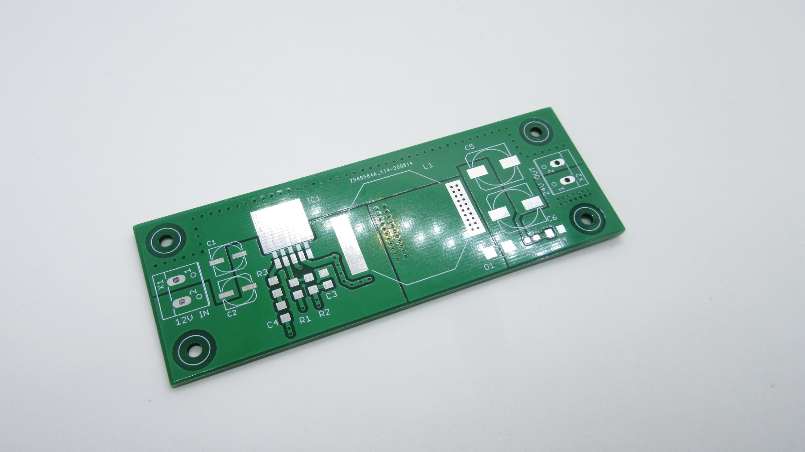
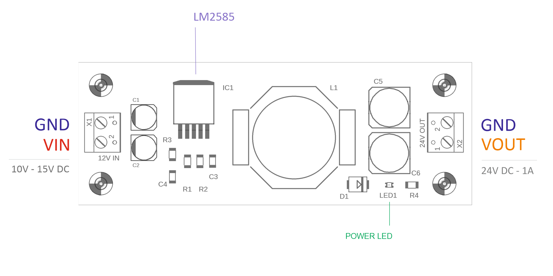
This is a DC-DC step-up converter based on LM2585-ADJ regulator manufactured by Texas Instruments. This IC was chosen for its simplicity of use, requiring minimal external components and for its ability to control the output voltage by defining the feedback resistors (R1,R2). NPN switching/power transistor is integrated inside the regulator and is able to withstand 3A maximum current and 65V maximum voltage. Switching frequency is defined by internal oscillator and it’s fixed at 100KHz.
The power switch is a 3-A NPN device that can standoff 65 V. Protecting the power switch are current and thermal limiting circuits and an under-voltage lockout circuit. This IC contains a 100-kHz fixed-frequency internal oscillator that permits the use of small magnetics. Other features include soft start mode to reduce in-rush current during start-up, current mode control for improved rejection of input voltage, and output load transients and cycle-by-cycle current limiting. An output voltage tolerance of ±4%, within specified input voltages and output load conditions, is specified for the power supply system.
Specifications
Vin: 10-15V DC
Vout: 24V DC
Iout: 1A (can go up to 1.5A with forced cooling)
Switching Frequency: 100KHz
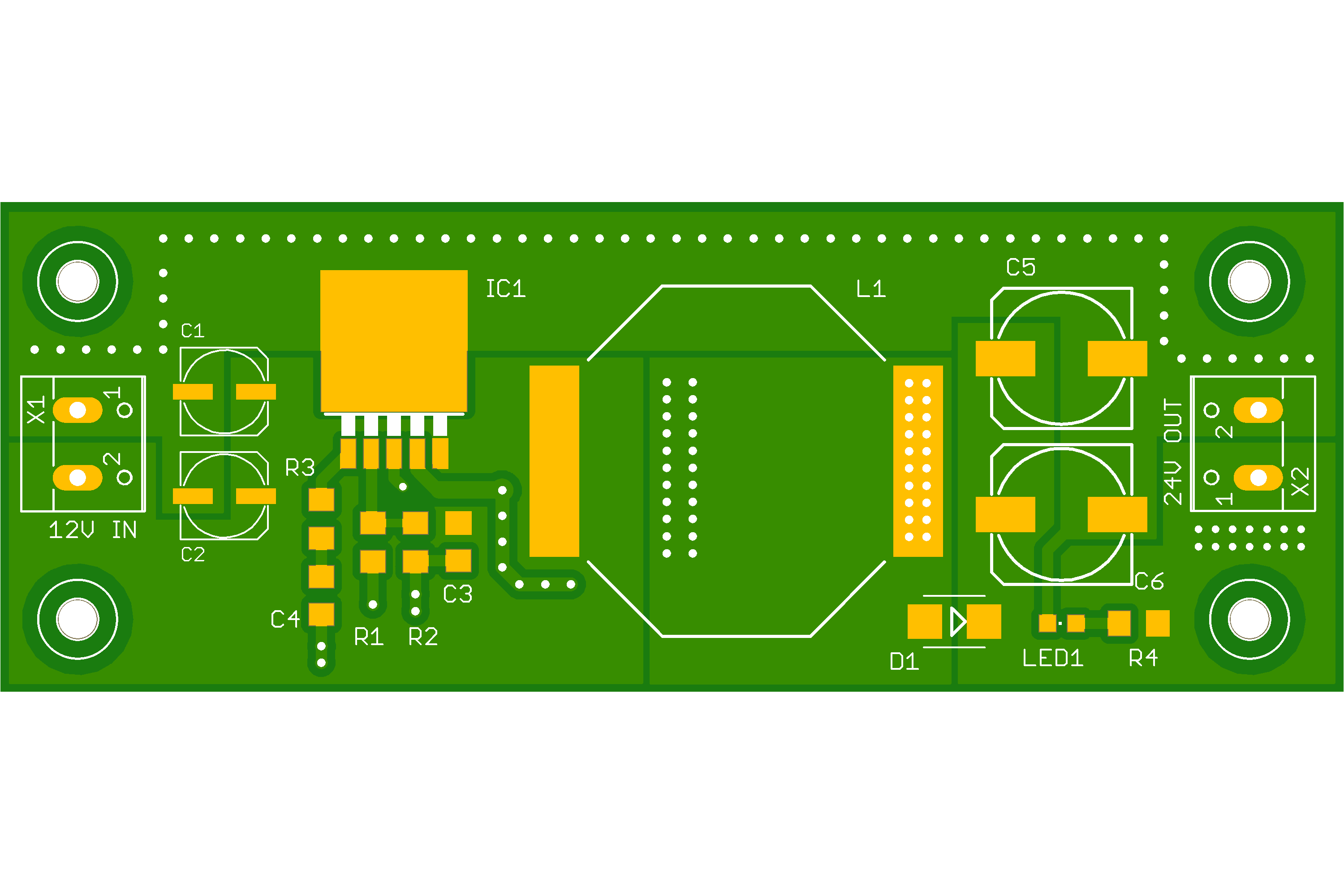
Schematic is a simple boost topology arrangement based on datasheet. Input capacitors and diode should be placed close enough to the regulator to minimize the inductance effects of PCB traces. IC1, L1, D1, C1,C2 and C5,C6 are the main parts used in voltage conversion. Capacitor C3 is a high-frequency bypass capacitor and should be placed as close to IC1 as possible.
All components are selected for their low loss characteristics. So capacitors selected have low ESR and inductor selected has low DC resistance.
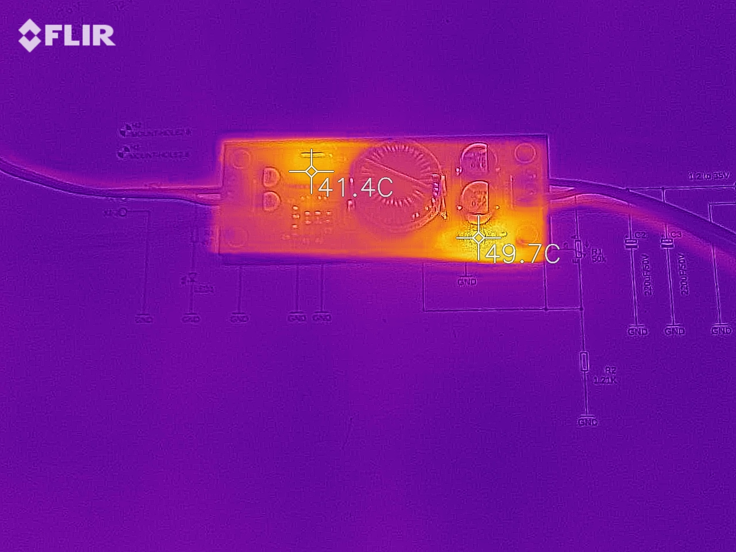
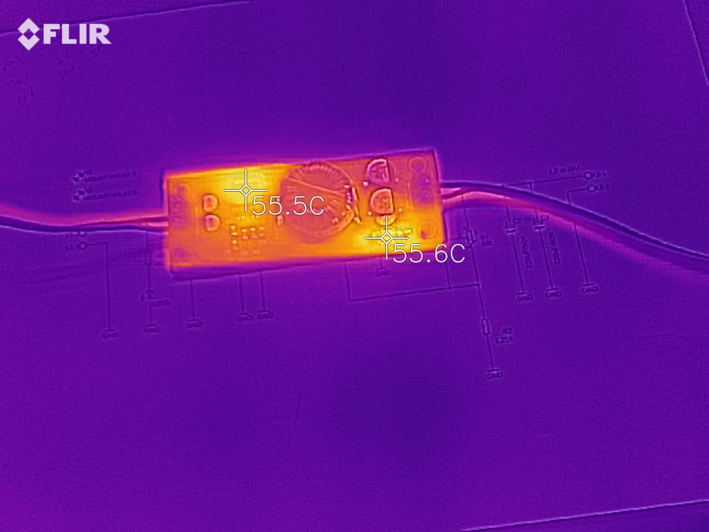
At maximum output power, there is significant heat produced by IC1 and for that reason, we mounted it directly on the ground plane to achieve maximum heat dissipation.
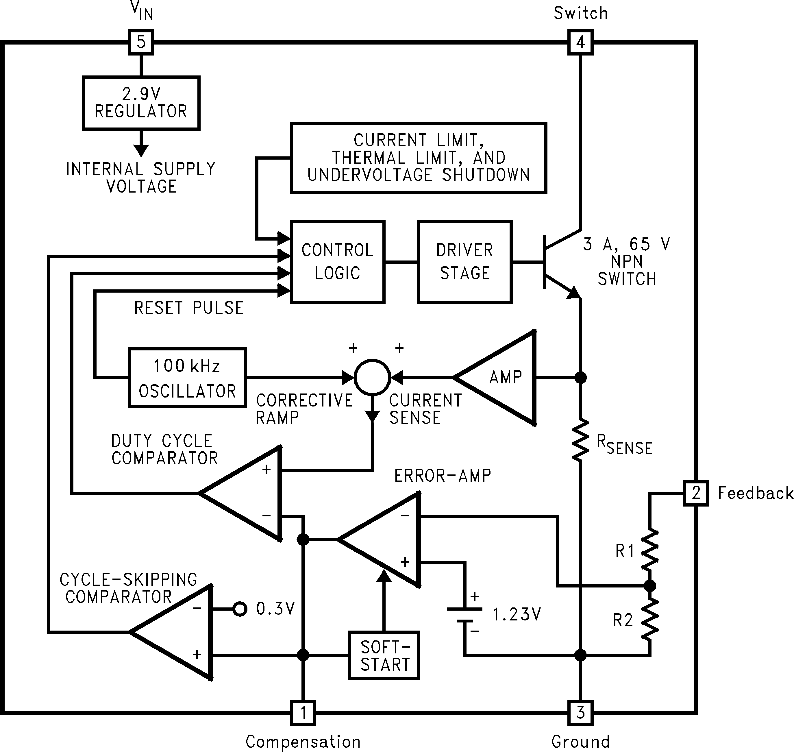
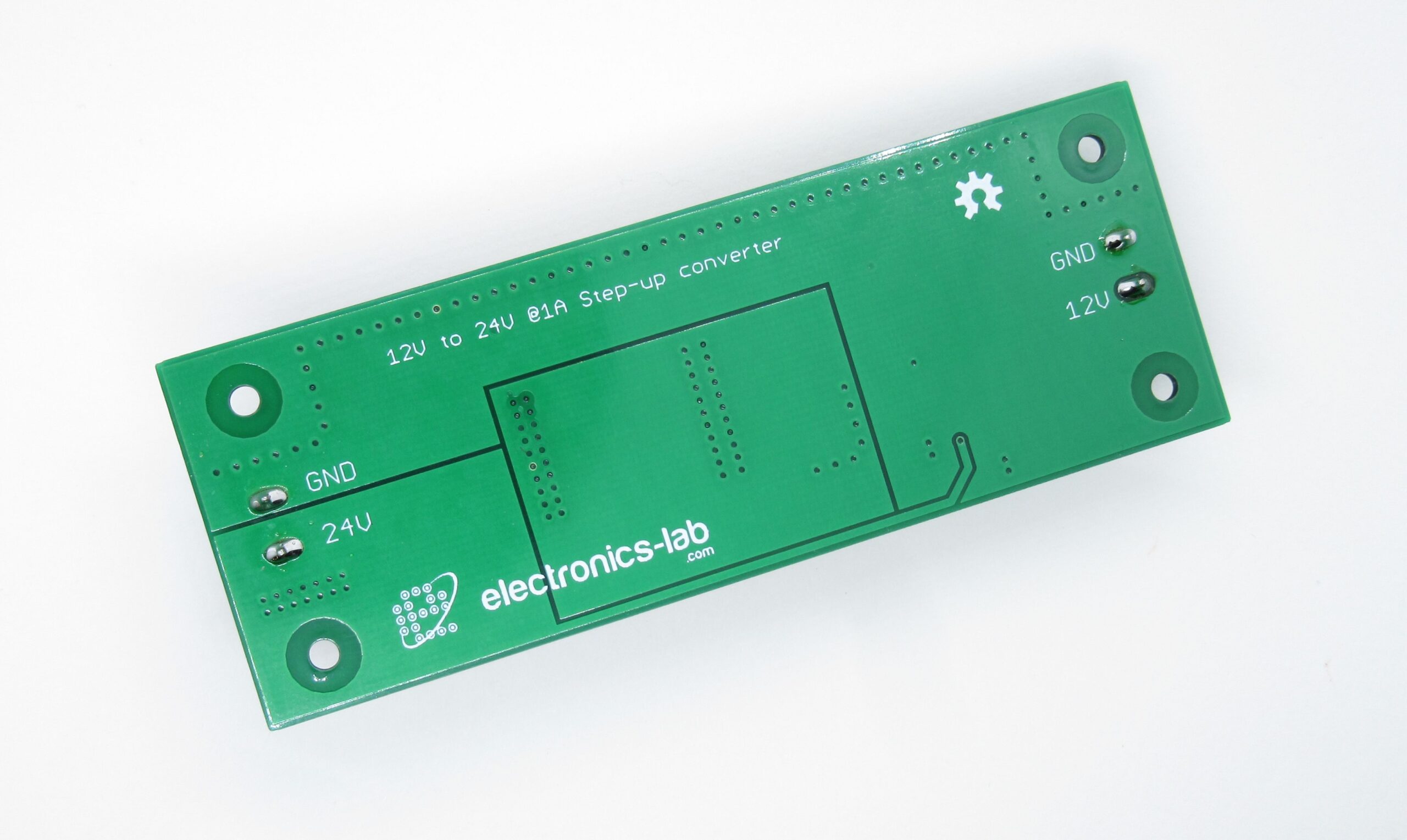
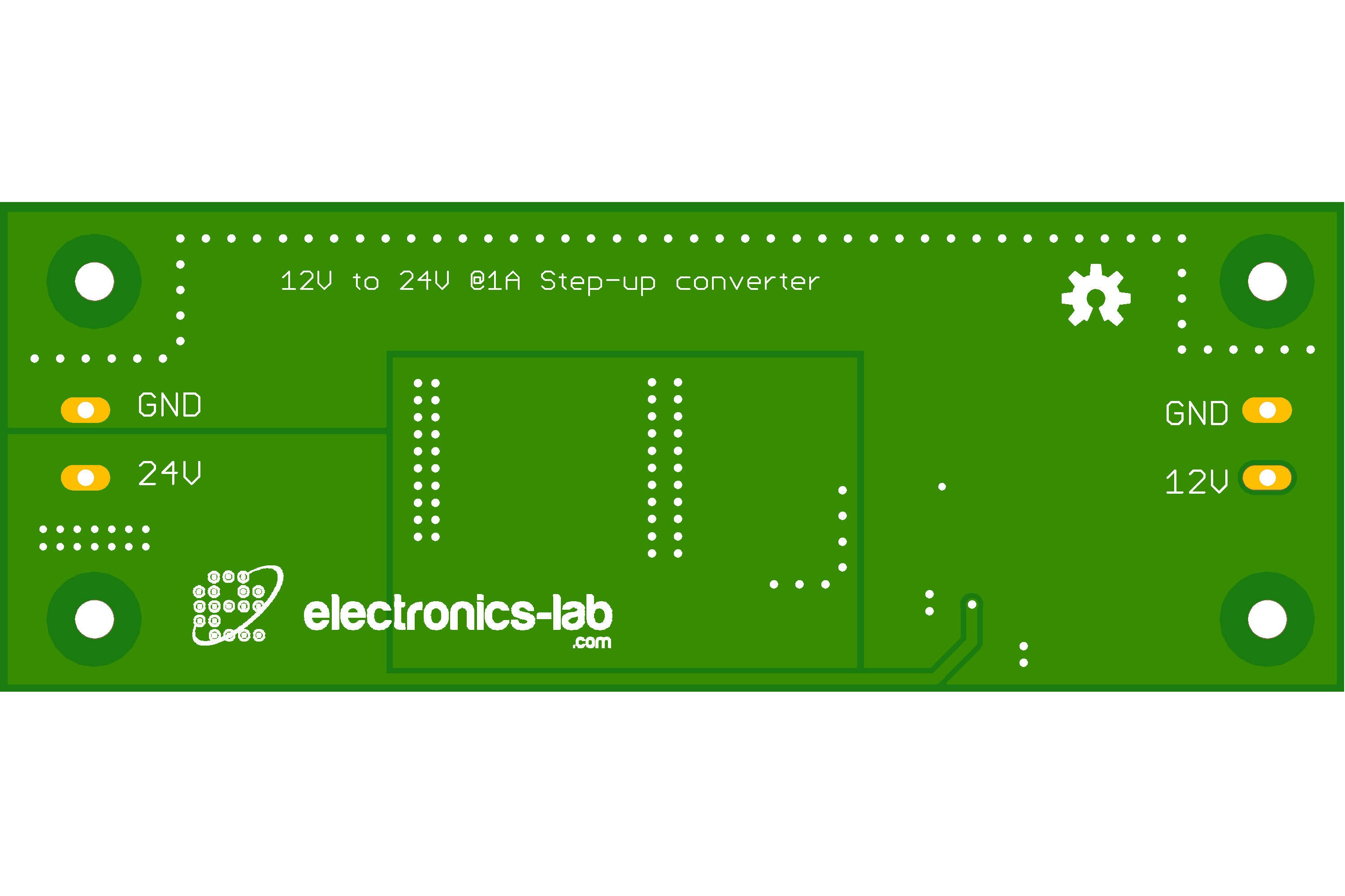
Block Diagram
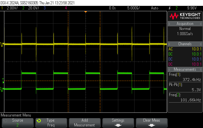
Measurements
CH1: Output Voltage ripple with 12V Input and 24V @ 500mA output – 5.3 Vpp – CH2: voltage at PIN 4 of IC1CH1: Output Voltage ripple with 12V Input and 24V @ 1A output – 4.6Vpp – CH2: voltage at PIN 4 of IC1
If you would like to receive a PCB, we can ship you one for 6$ (worldwide shipping) click here to contact us
Parts List
Part
Value
Package
MPN
Mouser No
C1 C2
33uF 25V 1Ω
6.3 x 5.4mm
UWX1E330MCL1GB
647-UWX1E330MCL1
C3
0.1uF 50V 0Ω
1206
C1206C104J5RACTU
80-C1206C104J5R
C4
1uF 25V
1206
C1206C105K3RACTU
80-C1206C105K3R
C5 C6
220uF 35V 0.15Ω
10 x 10.2mm
EEE-FC1V221P
667-EEE-FC1V221P
D1
0.45 V 3A 40V Schottky
SMB
B340LB-13-F
621-B340LB-F
IC1
LM2585S-ADJ
TO-263
LM2585S-ADJ/NOPB
926-LM2585S-ADJ/NOPB
L1
120 uH 0.04Ω
30.5 x 25.4 x 22.1 mm
PM2120-121K-RC
542-PM2120-121K-RC
R1
28 KΩ
1206
ERJ-8ENF2802V
667-ERJ-8ENF2802V
R2 R3
1.5 KΩ
1206
ERJ-8ENF1501V
667-ERJ-8ENF1501V
R4
1 KΩ
1206
RT1206FRE07931KL
603-RT1206FRE07931KL
LED1
RED LED 20mA 2.1V
0805
599-0120-007F
645-599-0120-007F
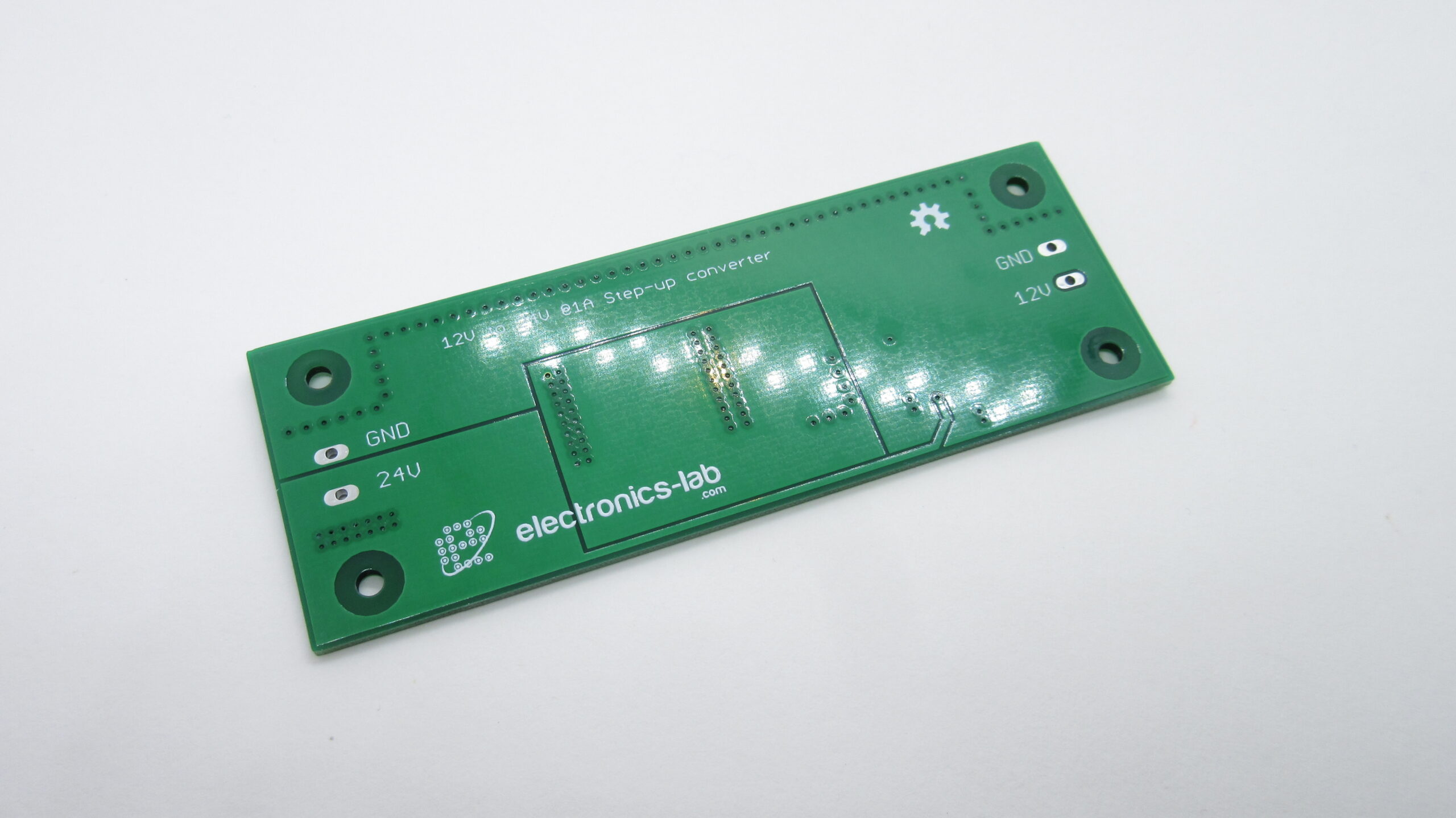
Connections
Gerber View
Simulation
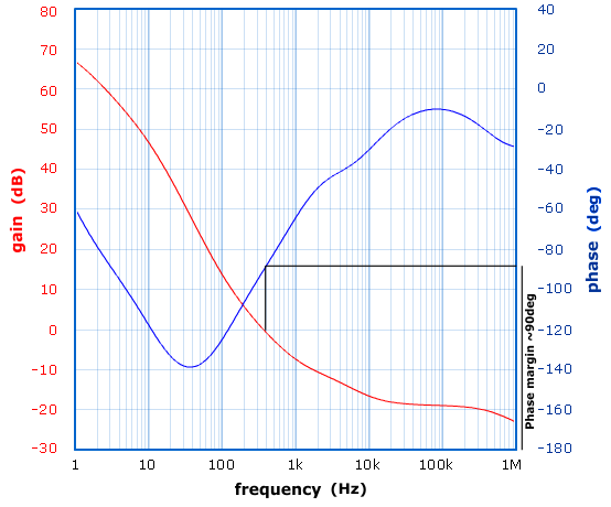
We’ve done a simulation of the LM2585 step-up DC-DC converter using the TI’s WEBENCH online software tools and some of the results are presented here.
The first graph is the open-loop BODE graph. In this graph, we see a plot of GAIN vs FREQUENCY in the range 1Hz – 1M and PHASE vs FREQUENCY in the same range. This plot is useful as it gives us a detailed view of the stability of the loop and thus the stability and performance of our DC-DC converter.
Bode plot of open control loop
What’s interesting on this plot is the “phase margin” and “gain margin“. The gain margin is the gain for -180deg phase shift and phase margin is the phase difference from 180deg for 0db gain as shown in the plot above. For the system to be considered stable there should be enough phase margin (>30deg) for 0db gain or when phase is -180deg the gain should be less than 0db.
On the plot above we see that the phase margin is ~90deg and that ensures that the DC-DC converter will be stable over the measured range.
The next simulation graph is the Input Transient plot over time.
Input Transient simulation
In this plot, we see how the output voltage is recovering when the input voltage is stepped from 10V to 15V. We see that 4ms after the input voltage is stepped the output has recovered to the normal output voltage of 24V.
The next graph is the Load Transient.
Load Transient simulation
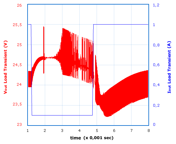
Load transient is the response of output voltage to sudden changes of load or Iout. We see that the output current suddenly changes from 0,1A to 1A and that the output voltage drops down to 23,2V until it recovers in about 3ms. We also see that when the load is reduced from 1A to 0,1A, output voltage spikes up to ~25,5V, then rings until it recovers to 24V in about 4ms.
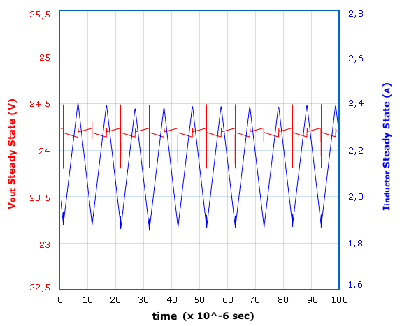
The last graph shows the Steady State operation of DC-DC converter @ 1A output.
This graph shows the simulated output voltage ripple and inductor current. We see that output voltage ripple is ~0,6Vpp and the inductor current has a peak current of 2,4A. The inductor we used is rated at max 5,6A DC so it can easily withstand such operating current and without much heating of the coil.
Operating point data (Vin=13V, Iout=1A)
Operating Values
Pulse Width Modulation (PWM) frequency
Frequency
100 kHz
Continuous or Discontinuous Conduction mode
Mode
Cont
Total Output Power
Pout
24.0 W
Vin operating point
Vin Op
13.00 V
Iout operating point
Iout Op
1.00 A
Operating Point at Vin= 13.00 V,1.00 A
Bode Plot Crossover Frequency, indication of bandwidth of supply
Cross Freq
819 Hz
Steady State PWM Duty Cycle, range limits from 0 to 100
Duty Cycle
48.3 %
Steady State Efficiency
Efficiency
93.2 %
IC Junction Temperature
IC Tj
65.2 °C
IC Junction to Ambient Thermal Resistance
IC ThetaJA
34.9 °C/W
Current Analysis
Input Capacitor RMS ripple current
Cin IRMS
0.14 A
Output Capacitor RMS ripple current
Cout IRMS
0.48 A
Peak Current in IC for Steady State Operating Point
IC Ipk
2.2 A
ICs Maximum rated peak current
IC Ipk Max
3.0 A
Average input current
Iin Avg
2.0 A
Inductor ripple current, peak-to-peak value
L Ipp
0.50 A
Power Dissipation Analysis
Input Capacitor Power Dissipation
Cin Pd
0.01 W
Output Capacitor Power Dissipation
Cout Pd
0.035 W
Diode Power Dissipation
Diode Pd
0.45 W
IC Power Dissipation
IC Pd
1.0 W
Inductor Power Dissipation
L Pd
0.16 W
Configuring Output Voltage
The output voltage is configured by R1, R2 according to the following expression (Vref=1,23V)
VOUT = VREF (1 + R1/R2)
If R2 has a value between 1k and 5k we can use this expression to calculate R1:
R1 = R2 (VOUT/VREF − 1)
For better thermal response and stability it is suggested to use 1% metal film resistors.
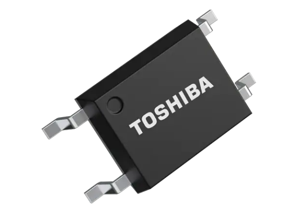
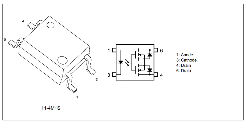
Toshiba Electronic Devices & Storage Corporation has introduced the TLP170AM and TLP170GM two new photorelays that can be used in security systems, which are used in building automation and other industrial equipment.
The TLP170AM has a rated OFF-state output terminal voltage of 60V and constant ON-state current (ION) of 0.7A with the pulse operation of up to 2.1A. The TLP170GM is a 350V version with an ION of 110mA constant current and 330mA pulse operation.
The new photo relays are designed with a maximum trigger LED current of 1mA for reducing the input-side power loss by increasing the sensitivity of the photodiode array. The devices provide lower power consumption and longer operation of devices when they are used in ON/OFF control in battery-powered security devices and various sensors.
The photo relays are packed in 4-pin SO6 Package, this provides a minimum isolation voltage of 3750Vrms allowing the devices to be used in equipment requiring high insulation performance. The new Photorelays are best suitable for security systems, Passive sensors, industrial equipment such as Programmable logic controllers, I/O interfaces, various sensor controls, etc. Building automation systems and in replacement of mechanical relays.
The X-CUBE-AZURE Expansion Package consists of a set of libraries and application examples for STM32L4 Series, STM32F4 Series, and STM32F7 Series microcontrollers acting as end devices.
X-CUBE-AZURE runs on four platforms. The B-L475E-IOT01A and 32F413HDISCOVERY boards support Wi-Fi® connectivity with an on-board Inventek module. The 32F769IDISCOVERY board provides a native Ethernet interface. The P-L496G-CELL02 pack includes an STM32L496AGI6-based low-power Discovery board equipped with Quectel’s BG96 modem (LTE Cat M1/NB/2G fallback) for cellular connectivity.
For the four platforms, a sample application configures the network connectivity parameters, and illustrates the various ways for a device to interact with Microsoft® Azure® IoT Hub. The application shows how a simple client application connects to the Azure® IoT Hub in order to publish device state and telemetry data, and receive device configuration from the cloud.
The application handles Azure® messages, methods and twin update commands. This allows, from the Azure IoT console, the remote control of the user LED state, the change of the telemetry interval, or the trigger of remote firmware update.
Key features
Ready-to-run firmware example using cellular, Wi-Fi®, and Ethernet connectivity to support quick evaluation and development of Microsoft® Azure® cloud-connected applications
Board configuration interface for connection to the Azure® IoT Hub
Secure Boot and Secure Firmware Update
TLS encryption
Azure® IoT Hub, and bidirectional communication examples implemented
Azure® X509 device authentication and Azure® Device Provisioning Service (DPS)
Connection to an Azure® IoT central demonstration
Connection to STMicroelectronics dashboard for Azure®, for easy sensor data visualization and device control
Specific features on the B-L475E-IOT01A board such as measurement of humidity, temperature, 3-axis magnetic data, 3-axis acceleration, 3-axis gyroscope data, atmospheric pressure, and time-of-flight
It connects to the ST-AZURE-Dashboard for easy sensor data visualization and device control. It is possible to securely update firmware based on a bootloader derived from the X-CUBE-SBSFU Expansion Package.
Device authentication and TLS encryption security features are complemented on the client side by the Secure Boot and Secure Firmware Update features.
The B-L475E-IOT01A board reports telemetry data such as measurement of humidity, temperature, and atmospheric pressure.
If you have developed your prototype on a Raspberry basis and are now looking for an adequate replacement, you will find it in the ND108T from ICP Germany. The industrial PICO-ITX board with only 100x72mm size is delivered with an ARM Cortex A53 processor from the NXP i.MX8M family. Available is a Quad Core and a Dual Core with 1.5GHz as well as three memory sizes of 1GB, 2GB and 4GB LPDDR4 SDRAM with 1600MHz clock rate. The eMMC memory is delivered preloaded with 8Gb, 16GB or 32GB. The ND108T’s memory can be expanded via a Micro SD card slot.
In the basic version, ND108T comes with HDMI 2.0 with 4K resolution, GbE, two USB 3.0, one USB 2.0, one RS-232/422/485, and audio line-out and mic-in. A USB 2.0 OTG or the UART is also available for programming and debugging. In addition to the standard Mini-PCIe with PCIe and USB signal, a Raspberry PI* compatible 40 pin header with GPIO signal is available as an expansion slot. For the 40 pin GPIO interface, the API library is available. If required, the basic version can be upgraded. Dual GbE or other display connectors like LVDS or Display Port are optionally available. The ND108T operates with a 12 Volt power supply in a temperature range of 0°C to 60°C and complies with the CE/FCC Class B standard. Both Yocto and Android are available as Board Support Packages for the ND108T.
*Raspberry Pi is a trademark of the Raspberry Pi Foundation