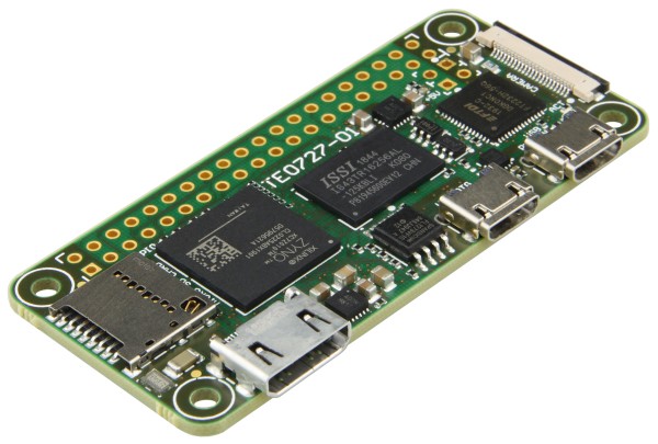
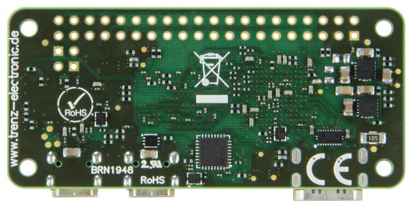
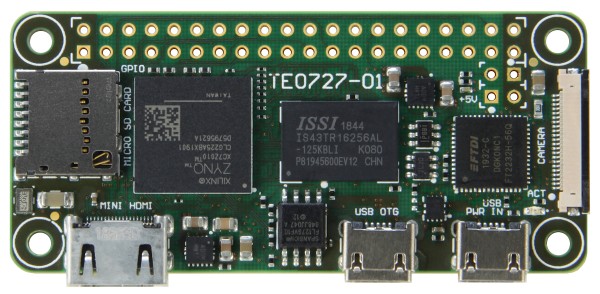
Germany Based Trenz Electronics, has released a new FPGA development board, a 3 x 6.5cm SoC module with integrated Xilinx Zynq-7010 FPGA and a Pi Zero form factor, called the ZynqBerryZero.
The Zyncberryzero
New ZynqBerryZero, nicknamed “little cousin” to older Zynqberry, is the latest addition to the company’s Raspberry Pi inspired FPGA lineup of boards. The ZynqBerryZero is actually raspberry pi-inspired like it’s an older cousin but can be used as an FPGA alternative to the Raspberry Pi Zero.
The ZynqberryZero packs it’s processing power punch with a Xilinx Zynq-7000 FPGA and a dual Arm Cortex-A9 MPCore, physically located in the middle of the FPGA’s programmable logic.
Some features of the ZynqberryZero include:
Xilinx Zynq-7010 FPGA
512 MB DDR3L SDRAM
16 MB flash memory
One microSD card slot
Two microUSB connectors: 1x micro USB for JTAG/UART and 1x micro USB 2.0
40 pin HAT header
Type C mini HDMI connector, and
CSI-2 connector.
Total GPIO: 26 (all provided by high-speed connectors)
Dimensions: 3cm x 6.5 cm
Operating temperature: Depends on customer design and cooling solution.
The ZynqberryZero module is currently available and sells for $149.74 (with shipping) or $129.09 (without shipping). Though the price looks like what could make the ZynqberryZero module quite the investment piece for projects, the module offers users quite a lot of features that make it totally worth it.
The power and flexibility of the FPGA’s capabilities in such a tight, well-designed layout make the ZynqberryZero a great option for a lot of projects. Having an onboard ARM processor surrounded by the programmable logic also means countless design options for the ZynqberryZero module.
The ZynqberryZero can from one of its micro USB ports instead of looking for an external power supply to use.
Displaying the versatility and compatibility features of the ZynqberryZero, Trenz in a recent demonstration showed that with a little tweak, the ZynqberryZero can be used interchangeably with a Pi Zero in projects. This is buttressed by the shared form factor which ensures compatibility with a majority of Raspberry Pi peripherals with little or no adaptation.
A reference design is not currently available for the ZynqberryZero but one can easily work out the pinout based on the available schematics and XDC generator files available on Trenz’s website.
The board is currently available on Trenz’s website for €109.00 excluding shipping. More details on the features and availability of the ZynqberryZero module can be found on the product’s sales page on Trenz’s Online Store.
Earthquakes are shifts or vibrations in the earth’s crust caused by a sudden release of violent energy and the effects that come with them, especially with the large ones, can be devastating. The earlier citizens are warned ahead of its occurrence, the better their chances of survival.
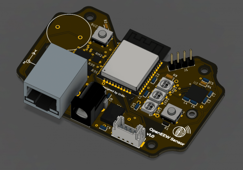
Fair enough, a number of earthquakes early warning systems already exist, but most of these systems are typically centralized and built on expensive equipment. The good news is that Grillo, a distributed sensor expert – in partnership with Linux Foundation and global tech giant, IBM – have open-sourced an IoT-based earthquake early warning system, believed to potentially save lives in the future, called OpenEEW.
Speaking about the origin of the project, Grillo founder, Andres Meira said,
“For years we have seen that EEWs have only been possible with very significant governmental financing, due to the cost of dedicated infrastructure and development of algorithms. We expect that OpenEEW will reduce these barriers and work towards a future where everyone who lives in seismically-active areas can feel safe.”
Speaking also on the OpenEEW being
“the very best in technology and open source”, was Mike Dolan, Senior Vice President and GM of Projects at the Linux Foundation. Dolan said the Linux Foundation is “pleased to be able to host and support such an important project and community”, adding that the OpenEEW project will accelerate the creation of low cost, community-driven projects across the world.
The OpenEEW, by contrast to other EEW systems, can run on a Raspberry Pi single-board computer with a bare-minimum outlay on additional hardware. It is based on low-cost high-performance MEMS accelerometers and is equal with professional seismometers in performance but 60 times less expensive. The sensor also has WiFi and Ethernet connectivity for sending readings back to the central server, a loud buzzer, and 3x bright Neopixel LEDs for alarming. The operating voltage is 3.3V with a current of 1A (maximum).
IBM on its own part, added a new dashboard for the Grillo’s earthquake sensor to visualize sensor readings and thereafter sent out six of the sensor systems to conduct tests in Puerto Rico. The company, through it’s Chief Technology Officer of Call for Code, Daniel Krook, said it will continue to collaborate with Grillo and the Linux Foundation to bring contributions to the openEEW project.
More information on the OpenEEW project including how to deploy your own sensors, detect earthquakes and send alerts, is available on the project’s website and on the project’s GitHub repository.
Arduino, the leading IoT product development platform, has announced it will make security best practices achievable by anyone by including them as standard in the popular, easy-to-use Arduino IoT Cloud solution. Specifically in the IoT space, operating without sophisticated security measures in place can put customers and their data at risk. Today, data, network, and device security remain the primary concern for 50% of organizations when adopting IoT. Arduino understands the risk of compromise and is constantly looking for ways to improve security in both its hardware and software, with a strong focus on “security by design”. Arduino IoT Cloud is a low-code platform that enables users to log, graph, and analyze their sensor data, trigger events, and automate their home or business.
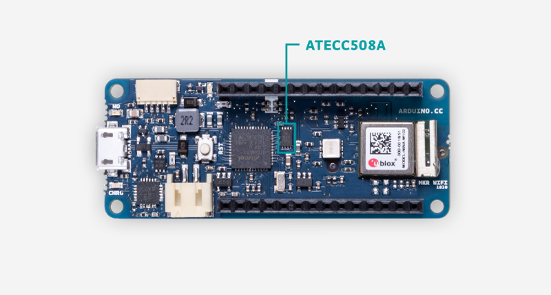
You can sign up for Arduino IoT Cloud for free today and now automatically benefit from integrated security features including: Secure communication with Arduino Portenta H7, Arduino Nano 33 IoT and Arduino MKR family boards using their on-board secure elements (NXP EdgeLock SE050 or Microchip ATECCX08A) The open-source ArduinoBearSSL library for implementing the TLS protocol on devices A device certificate provisioning process to allow client authentication during MQTT sessions.
Fabio Violante, CEO of Arduino said:
“Our priority has always been to build solutions that ensure maximum security for our users and developers and take every step to minimize risk. We are extremely proud of the development of a model that can make our solutions secure by design. As IoT devices continue to proliferate at pace, we will remain committed to finding even more ways to improve security for years to come.”
Many of today’s embedded devices still do not properly implement the full SSL/TLS stack. Optimized for constrained devices, ArduinoBearSSL aims at producing small code footprints and low RAM usage.
It provides developers with a sturdy foundation to their codebase that is fully interoperable with existing SSL/TLS servers. Security and performance was a focus when fitting the standard Bear SSL into Arduino’s embedded IoT core. Arduino IoT enabled boards to include one or more (as in the case of the Portenta H7) hardware crypto chips dedicated to the fast computation of cryptography operations. RAM is therefore free of these demanding tasks, private keys are stored securely, and true random number generation (a basic operation to ensure secure communications) can be delivered effectively.
Different communication techniques are put in motion behind the scenes to guarantee a point to point encrypted communication between the Arduino-powered IoT device and Arduino’s servers. Both techniques, asymmetric and symmetric encryption, facilitate a handshake between the client and the server, and issuing unique session keys. The process of device registration in the Arduino IoT Cloud has been simplified to help developers optimize their workflows. Arduino’s API exposes an endpoint a client can interact with, the client requests to register a new device on the Arduino IoT Cloud, to which the server (API) returns a UUID (Universally Unique IDentifier) that will be stored in the board’s crypto element. From that moment and on, developers can use that UUID in their code to identify their devices against the Arduino IoT Cloud. The device’s private key cannot be extracted by the secure element – a fundamental benefit of installing the IoT Cloud security model on official Arduino boards.
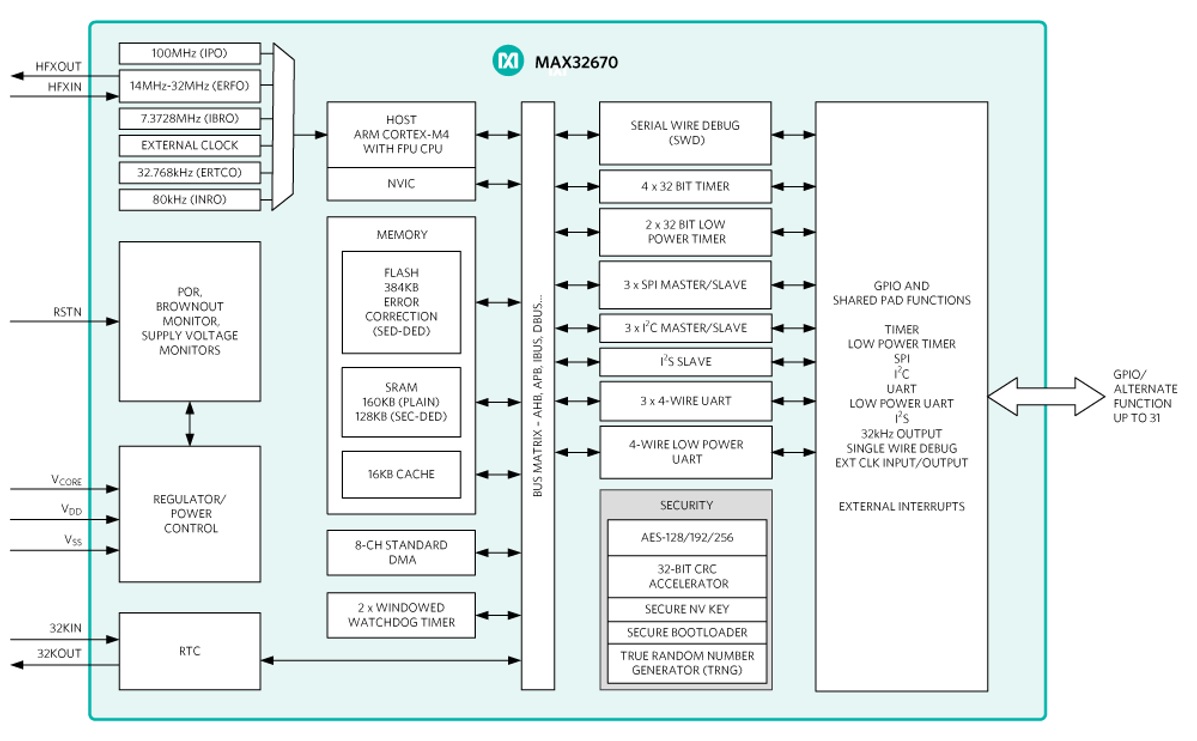
In the Darwin family, the MAX32670 is an ultra-low power, cost-effective, high reliability 32-bit microcontroller enabling designs with complex sensor processing without compromising battery life. It combines a flexible and versatile power management unit with the powerful Arm® Cortex®-M4 processor with floating point unit (FPU). The MAX32670 also offers legacy designs an easy and cost optimal upgrade path from 8- or 16-bit microcontrollers.
The device integrates up to 384KB of flash and 160KB of SRAM to accommodate application and sensor code. error correction coding (ECC), capable of single error correction and double error detection (SEC-DED), is implemented over the entire flash, RAM, and cache to ensure ultra-reliable code execution for demanding applications. Additional features such as the two windowed watchdog timers with fully flexible and independent clocking have been added to further enhance reliable operation. Brownout detection ensures proper operation during power-down and power-up events and unexpected supply transients.
Multiple high-speed peripherals such as 3.4MHz I²C, 50MHz SPI, and 4MBAUD UARTs are included to maximize communication bandwidth. In addition, a low-power UART is available for operation in the lowest power sleep modes to facilitate wakeup on activity without any loss of data. A total of six timers with I/O capability are provided, including two low-power timers to enable pulse counting, capture/compare and PWM generation even in the lowest power sleep modes. The device packs all this capability in tiny form factors: 5mm x 5mm 40-pin TQFN-EP and 1.7mm x 2.2mm 24-bump WLP packages.
Key features
High-Efficiency Microcontroller for Low Power, High Reliability Devices
Arm Cortex-M4 Core with FPU Up to 100MHz
384KB Flash Memory with Error Correction
160KB SRAM (128KB with ECC Enabled), Optionally Preserved in Lowest Power Modes
16KB Unified Cache with ECC
UART Bootloader
Dual or Single-Supply Operation
Ultra-Low 0.9–1.1V VCORE Supply Voltage
Internal LDO Operation from Single Supply 1.7V to 3.6V
Wide Operating Temperature: -40°C to +105°C
Flexible Clocking Schemes
Internal High Speed 100MHz Oscillator
Internal Low Power 7.3728MHz and Ultra-Low Power 80kHz Oscillators
14MHz to 32MHz Oscillator (External Crystal Required)
32.768kHz Oscillator (External Crystal Required)
External Clock Input for the Core
External Clock Input for the LPUART and LPTMR
Power Management Maximizes Uptime for Battery Applications
44µA/MHz Active at 0.9V Up to 12MHz
50µA/MHz Active at 1.1V Up to 100MHz
2.6µA Full Memory Retention Power in Backup Mode at VDD = 1.8V
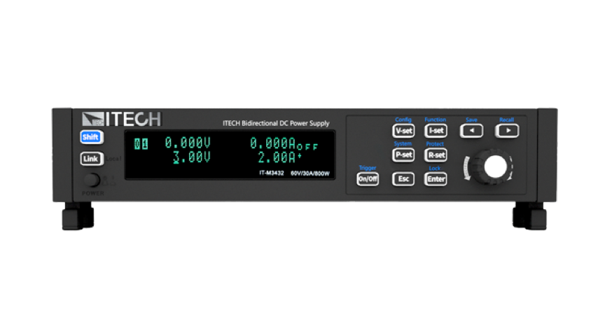
Released by ITECH in March 2020, the brand new series IT-M3400 Bidirectional DC Power Supply comes with cutting-edge technology which is integrated with engineers’ innovative inspiration. It integrates the features of a bidirectional power supply and a regenerative load. Meanwhile, it is also eco-friendly, helps to eliminate the heat dissipation to a minimum level and save your cost as well. IT-M3400 can fully contribute to environmental protection by reducing CO2 emissions.
The compact ITECH M series, ½ wide 19″rack module of 1U high, are available in four different voltage ranges (0-60V, 150V, 300V and 600V) at power ratings of 200W, 400W and 800W.
The full range of models supports multiple units stacking and parallel connection by easy design “legs” plug-in. Fit with rack mount kit to achieve the perfect use.
SOURCING & SINKING
The most important feature of the ITECH IT-M3400 Ultra Compact Bi-directional DC power supplies is the integration of the functionality of a bi-directional power supply and a regenerative electronic load. The unit automatically switches between power supply and load at lightning speed according to the circumstances, without overshooting current and voltage. Its regenerative character also makes the IT-3400 an enormously efficient power supply. The absorbed DC power is converted to AC and fed back into the grid with an efficiency of 90%. As a result, considerable savings can be made on air conditioning and electricity costs.
SIMULATE AND TEST BATTERY CELLS
With the standard software it is possible to easily charge and discharge the battery. With the extensive ITS5300 software you can also perform extensive drive cycle testing, life cycle testing, IR testing etc. In cooperation with the extensive BSS2000 battery simulation software, the IT-M3400 power supply is ideal for simulating battery modules. Specific properties of the battery can be programmed and thus the electronics around the battery can be tested. The specific battery conditions are then very easy to simulate.
MULTI CHANNEL ATS SYSTEMS
Thanks to the ability to connect different IT-M3400 power supplies in parallel, a wide power range can be covered. Also, up to 16 channels can be controlled independently or synchronously with a single interface. The compact design makes the IT-M3400 an excellent candidate for installation in automatic test systems to perform multi-channel tests. Ideal for large-scale testing of power electronics such as IGBT Power Modules or bi-directional DC/DC converters commonly used in electric vehicles. The IT-M3400 series is available with common I/O interfaces and compatible with most communication protocols.
Besides, IT-M family includes IT-M3100 Ultra-compact Wide Range DC Power Supply, IT-M3200 High Precision Programmable DC Power Supply, IT-M3300 Regenerative DC Electronic Load, IT-M3600 Regenerative Power System, IT-M7700 Programmable AC Power Supply. Learn more about ITECH products and solutions, please visit https://www.itechate.com
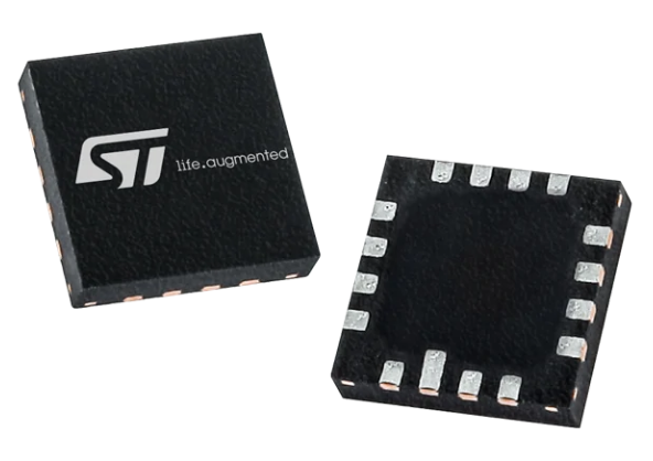
STMicroelectronics’ high-accuracy and low-power two-axis linear accelerometer includes digital output.
The STMicroelectronics IIS2ICLX is a high-accuracy (ultra-low noise, high stability and repeatability) and low-power two-axis linear accelerometer with digital output. The IIS2ICLX has a selectable full scale of ±0.5/±1/±2/±3 g and is capable of providing the measured accelerations to the application over an I²C or SPI digital interface. Its high accuracy, stability over temperature and repeatability make IIS2ICLX particularly suitable for inclination measurement applications (inclinometers).
The sensing element is manufactured using a dedicated micromachining process developed by STMicroelectronics to produce inertial sensors and actuators on silicon wafers. The IC interface is manufactured using a CMOS process that allows a high level of integration to design a dedicated circuit which is trimmed to better match the characteristics of the sensing element. The IIS2ICLX has an unmatched set of embedded features (programmable FSM, Machine Learning Core, sensor hub, FIFO, event decoding, and interrupts) which are enablers for implementing smart and complex sensor nodes that deliver high accuracy and performance at very low power.
Features
2-axis linear accelerometer
Selectable full scale: ±0.5/±1/±2/±3 g
Ultra-low noise performance: 15 µg/√Hz
Superior stability over temperature (<0.075 mg/°C) and repeatability
Embedded compensation for high stability over temperature
I²C/SPI digital output interface
Low power: 0.42 mA with 2 axes delivering full performance
Sensor hub feature to efficiently collect data from additional external sensors
Smart embedded FIFO up to 3 kbytes
Programmable high-pass and low-pass digital filters
Programmable Machine Learning Core to integrate AI algorithms and reduce power consumption at system level
Programmable Finite State Machine to process data from accelerometer and one external sensor
Extended operating temperature range (-40°C to +105°C)
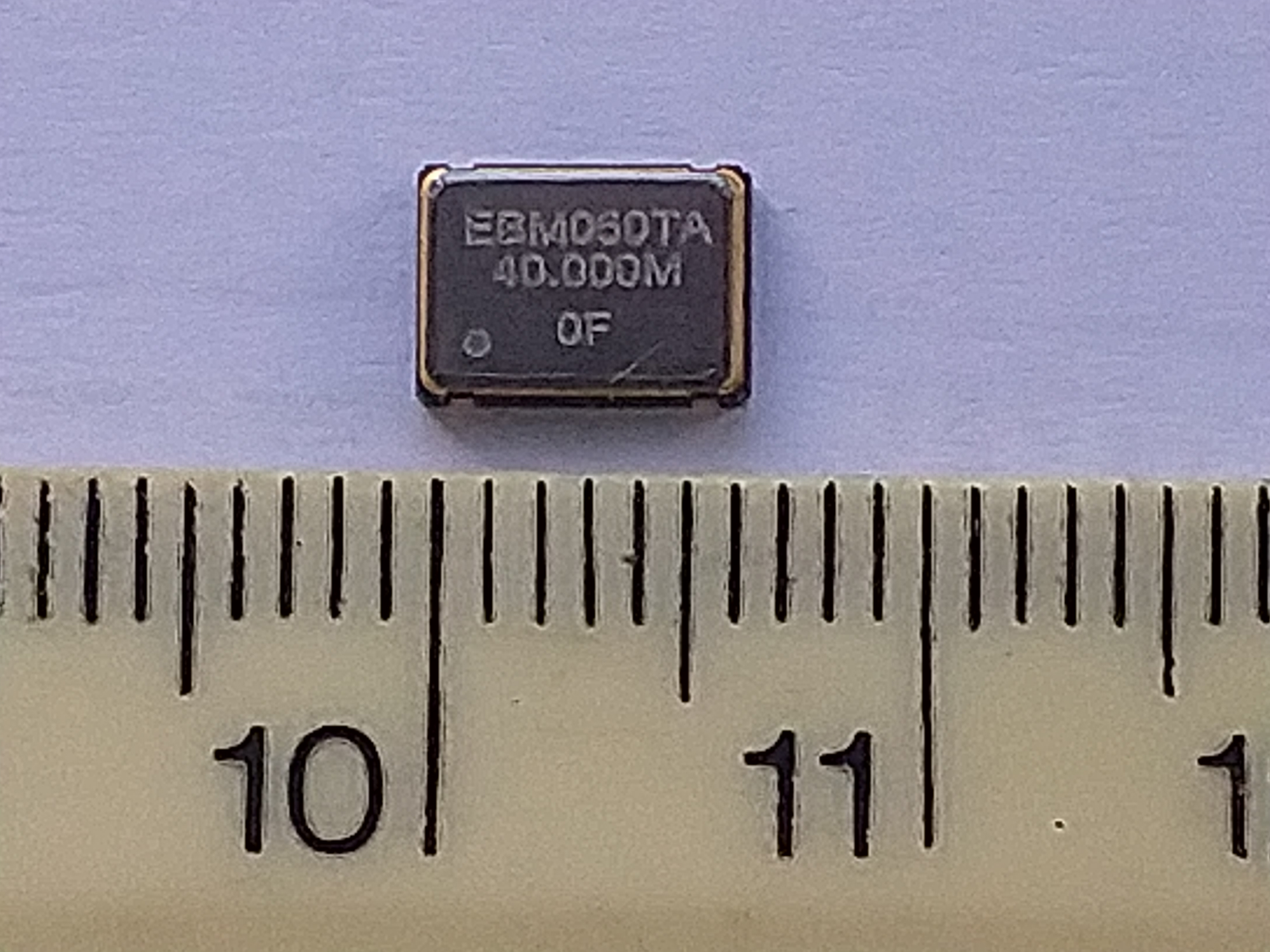
The EQXO-75UIE series is a ruggedized high-reliability, high temperature range clock oscillator in a standard format 7x5mm SMD ceramic package designed for demanding and vibrating industrial applications
Saelig Company, Inc. has launched the Euroquartz EQXO-75UIE Extended Industrial Temperature Ruggedized High-Reliability Oscillators. The EQXO-75UIE series is a ruggedized high-reliability SMD clock oscillator. Designed for demanding industrial applications, it provides reliable operation with excellent frequency stability across an extended industrial operating temp range of -40degC to +105degC. Mechanical shock survivability has been tested to 1500G MIL-STD-883K Meth 2002.5, Condition B. Temperature stabilities of ±50, 75 & 100ppm are available, with tighter options by request (dependent on conditions). This component, available with short lead time, has no ITAR restrictions. All EQXO-75UIE crystals are pre-aged as part of an additional manufacturing process in order to improve long-term application stability. With an aging specification of ±1ppm maximum for the first year, an even tighter aging specification is available by request.
EQXO-75UIE SeriesFeatures
Frequency Range: 2.00MHz to 60.00MHz
Operating Temperature: -40degC to 105degC
Shock Survivability: 1500G
Supply Voltages: 2.5V, 3.3V and 5V
Crystal Stabilization: 96 hours at 100degC
ITAR Restriction: none
If phase noise is a critical project design consideration then it is important to realize that vibration causes a degradation in both spectral output and phase noise. Even moderate levels of vibration can significantly introduce an unwanted signal variation. The acceleration-sensitivity (“g-sensitivity”) of components is often a limiting factor in these applications, and quartz crystals often prove to be a critical limiting component in a design.
The EQXO-75UIE Series of ruggedized, high-reliability, high temperature clock oscillators are made by European frequency product specialist Euroquartz, an independent UK-based manufacturer and supplier of quartz crystals, oscillators, filters and frequency-related products to the worldwide electronics industry. The company is AS9100 registered and designs and manufactures a comprehensive range of frequency control components for a wide range of customers for military and aerospace, communications, general electronics, computing, control systems and petrochemical applications. The EQXO-75UIE Series is available now from Euroquartz’ USA technical distributor Saelig Company, Inc.
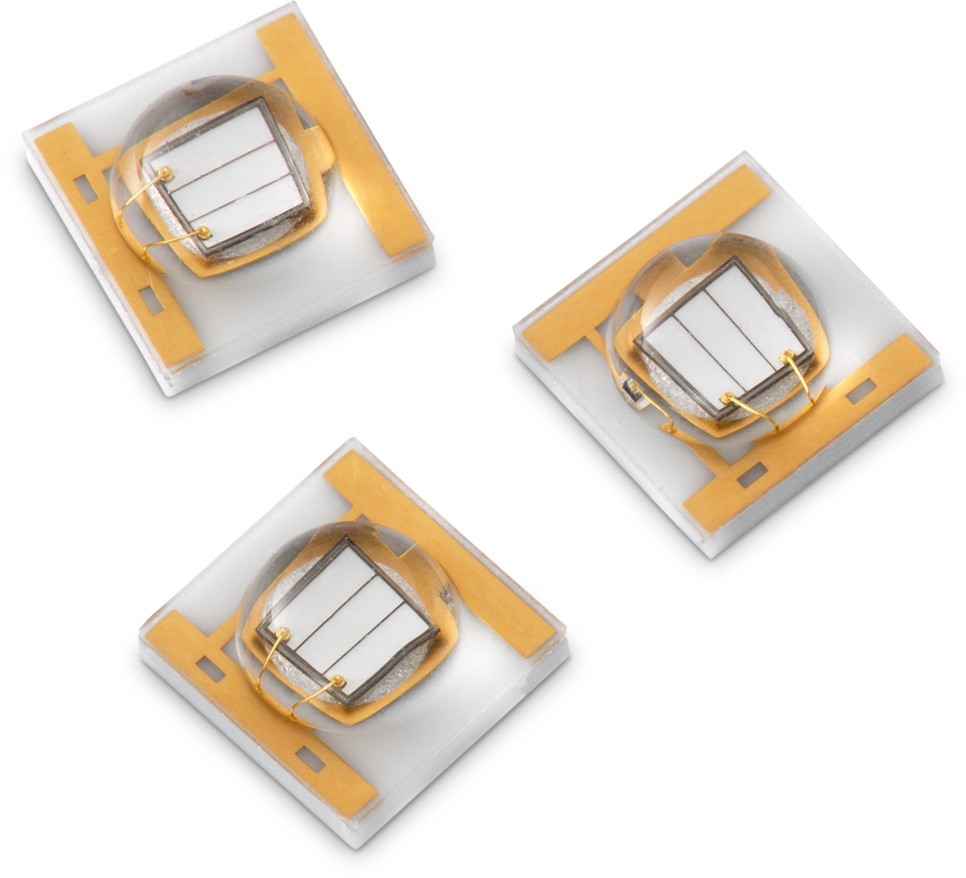
Würth Elektronik High Power Ultraviolet LEDs deliver high intensity UV output in a compact, industry-standard, 3535 ceramic package. Available with 385nm, 395nm, and 405nm peak outputs, these LEDs are an ideal choice for UV systems for curing, printing, and adhesive coating. These LEDs can also be used for high current applications such as special lighting, counterfeit detection systems, and security forensics tools. Würth Elektronik UV LEDs are a perfect upgrade from traditional mercury-vapor (Hg) lamps in these applications, offering faster turn-on time, higher power output, and a longer lifetime.
In the introduction tutorial Operational Amplifier Basics, we have briefly seen that from the same op-amp, many configurations leading to different functions can be adopted, depending on how the feedback loop is designed.
In this new tutorial, we propose to detail the most common configurations along with their function.
We chose to group the configurations in three distinct major groups which will constitute the sections of this tutorial. The first section will, therefore, focus on the buffer designs,
The second section presents the amplifier configurations whose goal is to amplify a signal. Finally, the third section presents the operational op-amps which transform one or more signals to perform elementary mathematical operations.
Buffer configurations
A buffer amplifier is a block that is placed between two circuits which impedances are not matching: a high (resp. low) output impedance connected to a low (resp. high) input impedance. The goal of the buffer is to insulate the stages from each other and perform an impedance adaptation.
Since our tutorial concerns op-amps, we will only talk about voltage buffers but there are also current buffers.
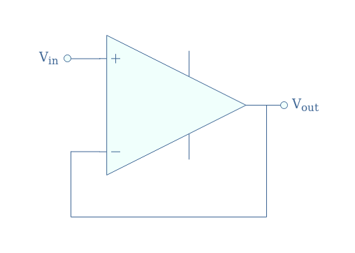
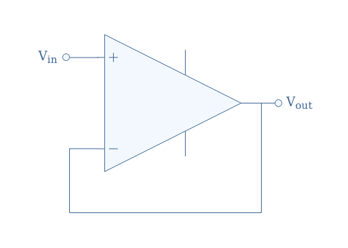
Voltage follower
The voltage follower is a buffer that does not amplify nor inverts the signal. Consequently, its gain is equal to +1. The design of the voltage follower is very simple and simply consist of a short-circuit feedback to the inverting input (-) of the op-amp:
fig 1: Voltage follower circuit
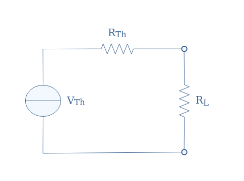
In order to really understand the purpose of this circuit, consider a Thevenin sourceVThwith an internal series resistance RTh that supplies an output load RL such as shown in Figure2:
fig 2: Thevenin source driving a load
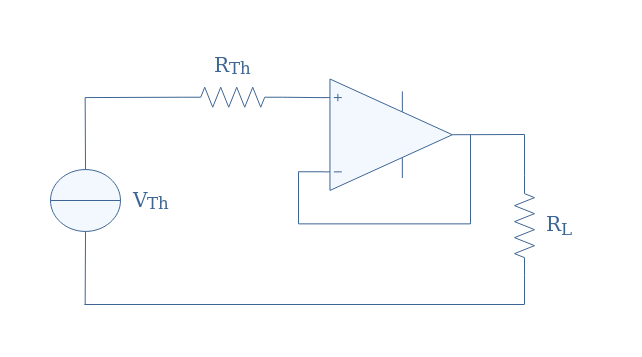
Due to the voltage division phenomenon, the source (VTh, RTh) will only be able able to provide a voltage VThRL/(RL+RTh) to the load. Let’s now place a voltage follower circuit between the source and the load:
fig 3: Voltage follower in a Thevenin circuit
If we label Zin the input impedance of the op-amp, the voltage provided to the amplifier is Vin=VThZin/(Zin+RTh). However, since the input op-amp impedance is very high (Zin>>RTh), or even infinite if we consider the amplifier to be ideal, the input voltage in the op-amp can actually be simplified to Vin=VTh.
Since the voltage follower has a gain of +1, the output voltage is Vout=VTh. The voltage provided to the load can be written VThRL/(RL+Zout), however, the output impedance (Zout) of an op-amp is very low (Zout<<RL) or even equal to zero if we consider the op-amp to be ideal. As a consequence, the voltage provided to the load can be simplified to VTh.
In that example, we can see that the voltage VTh is entirely provided to the output load without any division phenomena thanks to the voltage follower. The circuit shown in Figure 3 actually acts as an ideal voltage source with zero Thevenin internal resistance.
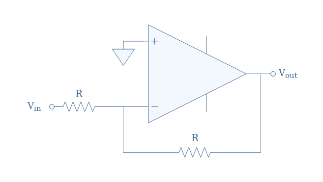
Inverting buffer
If we consider the circuit in Figure 1, add resistors in the feedback loop and inverting input, and connect the non-inverting input to the ground, we obtain a circuit known as inverting buffer:
fig 4: Inverting buffer circuit
Assuming that the value of the resistors is strictly identical under the working condition of the op-amp, the gain of this circuit is -1. The signal is therefore not amplified but inverted: Vout=-Vin.
Amplifier configurations
In this section, we present some configurations for which the op-amp act as an amplification device, meaning that Vout>Vin.
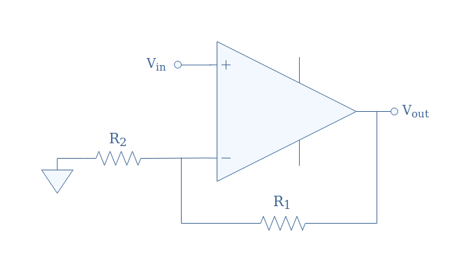
Non-inverting amplifier
We consider a similar circuit to the one presented in Figure 4, the resistors are, however, not necessarily of similar value and the input signal is provided to the non-inverting input (+):
fig 5: Non-inverting amplifier circuit
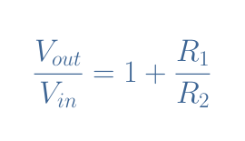
The gain Vout/Vin of the non-inverting amplifier is always strictly higher than +1 and given by Equation 1:
eq 1: Non-inverting amplifier gain
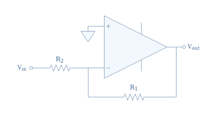
Inverting amplifier
The inverting amplifier is designed by grounding the non-inverting input and applying the signal to the inverting input in the circuit presented in Figure 5.
fig 6: Inverting amplifier circuit
The gain is given here by the ratio -R1/R2, the negative sign assures that the signal is inverted.
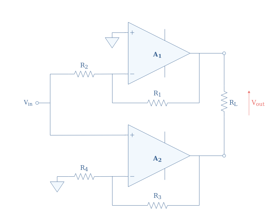
Bridge amplifier
An inverting and non-inverting amplifier can be connected together to form a bridge amplifier. In this circuit, the input is common to both amplifiers while the output is taken on a load RL that is connected between the outputs of the amplifiers.
fig 7: Bridge amplifier circuit
According to the previous subsections, the output of the first amplifier will be A1Vin with A1=-R1/R2. The output of the non-inverting amplifier is A2Vin with A2=1+(R3/R4).
Finally, with the direction convention chosen for Vout, the output of the bridge amplifier is given by (A1-A2)Vin. We can note that if the resistors are appropriately chosen, the magnitudes of the gain can be equalized (|A1|=|A2|), which allows the bridge amplifier to increase by a factor 2 the maximal amplification that a single amplifier could perform.
The advantage of the bridge amplifier is to be able to supply more power to an output load, by a factor 4. Moreover, a single-supply is able to drive both amplifiers that constitute the bridge amplifier, thus simplifying the design and cost of the circuit.
Operational configurations
Some op-amps configurations can perform elementary mathematical operations. In the following, we present the adder/subtractor and the derivator/integrator circuits.
Adder/subtractor
The adder configuration takes several voltages on its inverting input connected via resistors.
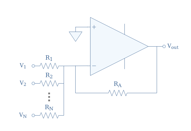
fig 8: Adder circuit with N inputs
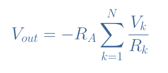
In the general case, the voltage Vout satisfies Equation 2:
eq 2: Adder configuration formula
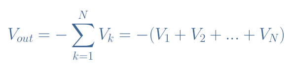
It is interesting to equalize all the resistances RA=R1=…=RN, which leads to a simplified formula where we can clearly see that the configuration presented in Figure 8 effectively adds the voltages:
eq 3: Simplified adder configuration formula
Note that the presence of the minus sign means that the voltage sum is inverted. In order to add the voltages without an inversion, we can simply place an inverting buffer after this stage.
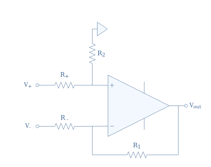
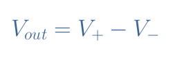
To realize a subtractor configuration, both the inverting and non-inverting output are used such as shown in Figure 9:
fig 9: Subtractor circuit
The configurations become again interesting when the resistor values are appropriately chosen so that R–=R1 and R+=R2. In that case, the subtractor function can be performed:
eq 4: Subtractor configuration formula when R–=R1 and R+=R2
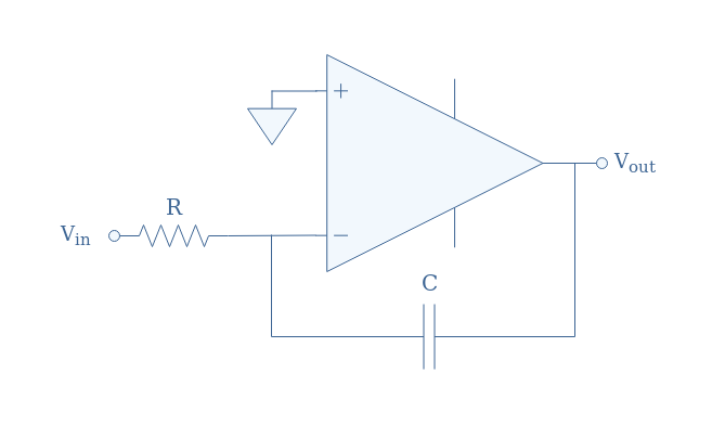
Derivator/Integrator
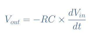
We start with the derivator which input is connected via a capacitor to the inverting branch, the feedback loop is connected with a resistor:
fig 10: Derivator circuit
The output is proportional to the variations of the input signal given by the derivative function:
eq 5: Derivator configuration formula
Derivators are useful to control the variations of certain physical parameters previously transformed in an electrical signal such as the temperature, pressure…
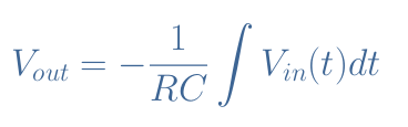
By inverting the position of the capacitor and resistor in Figure 10, we obtain the circuit of an integrator:
fig 11: Integrator circuit
For this circuit, the output is proportional to the integral of the input:
eq 6: Integrator configuration formula
Conclusion
We have presented in this tutorial some of the most important building blocks that can be realized with operational amplifiers. We chose to distinct these configurations in three groups depending on their function.
In the first section, we focused on the buffer configurations which do not amplify or modify the signal. The buffers can either be non-inverting (Vout=Vin) or inverting (Vout=-Vin) depending on which input the signal is applied. Thanks to their high input and low output impedances, buffers are mainly used to connect unmatching circuits together.
Amplifier configurations are presented in the second section with again, a distinction being made between inverting and non-inverting amplifiers. In both cases, it is the values of the resistors connected to the inverting branch that will dictate how much the output signal will be amplified. To conclude this section, we have presented the bridge amplifier which consists of interconnecting an inverting and non-inverting amplifier in order to increase the power that can be supplied to the output load.
Finally, operational configurations that can perform elementary mathematical operations are presented in the last section. An adder amplifier can be realized with an inverting op-amp with multiples inputs, a subtractor is realized with inputs on both inverting and non-inverting inputs. In both cases, it is interesting to equalize the resistors present in the circuit in order to realize additions and subtractions with any prefactor. Moreover, integrator and derivator designs are presented, they both have a capacitor in their design and are used either to integrate or derivate the input signal, these functions are widely used in automation.
AAEON and AOTU.AI are excited to announce the launch of the BrainFrame Edge AI Developers Kit (DevKit) on an Intel AI platform for IoT that will allow developers and system integrators to rapidly create and deploy Smart Vision applications.
AI computer (smart) vision applications are often bespoke and laborious to build and deploy. The BrainFrame Edge AI DevKit provides a new paradigm in creating solutions such as vision-based access control, uniform compliance, manufacturing automation, and video analytics.
AAEON’s fanless industrial computer is powered by 8th Generation Intel® Core™ i5 Processors and Intel® Movidius™ Myriad™ X VPU and pre-installed with the Aotu.ai BrainFrame™ Smart Vision platform.
BrainFrame™ is a platform designed to be easy to scale and highly configurable to allow any connected camera to become a continuously monitoring Smart Vision system. BrainFrame’s automatic algorithm fusion and optimization engine is powered by VisionCapsules™, Aotu.ai’s open source algorithm packaging format. These self-contained capsules have a negligible memory footprint and include all necessary code, files, and metadata to describe and implement a machine learning algorithm.
VisionCapsules enable drag and drop Smart Vision AI algorithms and provides complete support for the Intel Distribution of OpenVINO™ toolkit. The deep integration of the OpenVINO toolkit fully leverages the optimization and acceleration offered by the toolkit on Intel’s processors.
Stephen Li, CEO of Aotu.ai, explains,
“we built BrainFrame when we saw how fragmented the Smart Vision AI ecosystem is and how complex it was to create and deploy a system. We realized there is an opportunity for a platform that can become the “Android OS” of video cameras where you can download algorithms as easy as downloading Android applications.”
“With Intel’s 8th Generation Core processors and Myriad X VPU, the DevKit provides outstanding performance and value for developers needing the computational power for their applications,” said Jason Lu, Product Manager with AAEON North America. “Paired with Aotu.ai’s BrainFrame provides for immense expandability and support for AI applications, while removing unnecessary complexities during the development process.”
“AI is transforming the IT industry, and Smart Vision is one of the leading drivers of that transformation. The Aotu.ai and Aaeon solution on Intel’s platform is operationalizing and accelerating the deployment of AI-based Smart Vision in the ecosystem.” said Dr. Cormac S.G. Conroy, Board Member, Aotu.ai.