As we have featured earlier this month the Selpic P1 is going to launch on Indiegogo in late July. But what is Selpic P1? Is it another handheld printer going around or it has something more to offer?
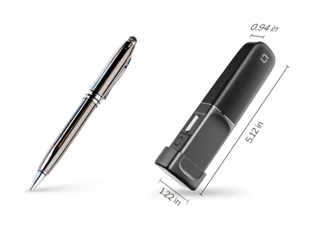
Selpic claims this to be the world’s smallest Handheld Portable printer that enables you to print on almost any surface like using an ordinary pen. It’s highlights include:
Lightweight and Portable
Print Anything, Anywhere
600dpi print resolution
90 pages of ink capacity (5% in coverage)
up to 6 colors to choose from
3 hrs working time per charge
With its pen styled shape, you can carry it around with you and get ready to use it anytime. It can easily print text, images, graphics,QR codes, and barcodes even on porous surfaces. The print head features 300 tiny nozzles with 0.002 of nozzle spacing and each nozzle can eject 18m drops per second. This leads to a high-quality and clear print result in printing logos or anything else on almost any surface.
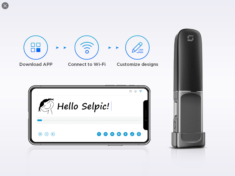
The printer comes along with a user-friendly smartphone APP that lets you define the print artwork. All you have to do is to connect the Selpic P1 with your smartphone over wifi and then you are ready to edit the artwork and print.
Hands-on Review
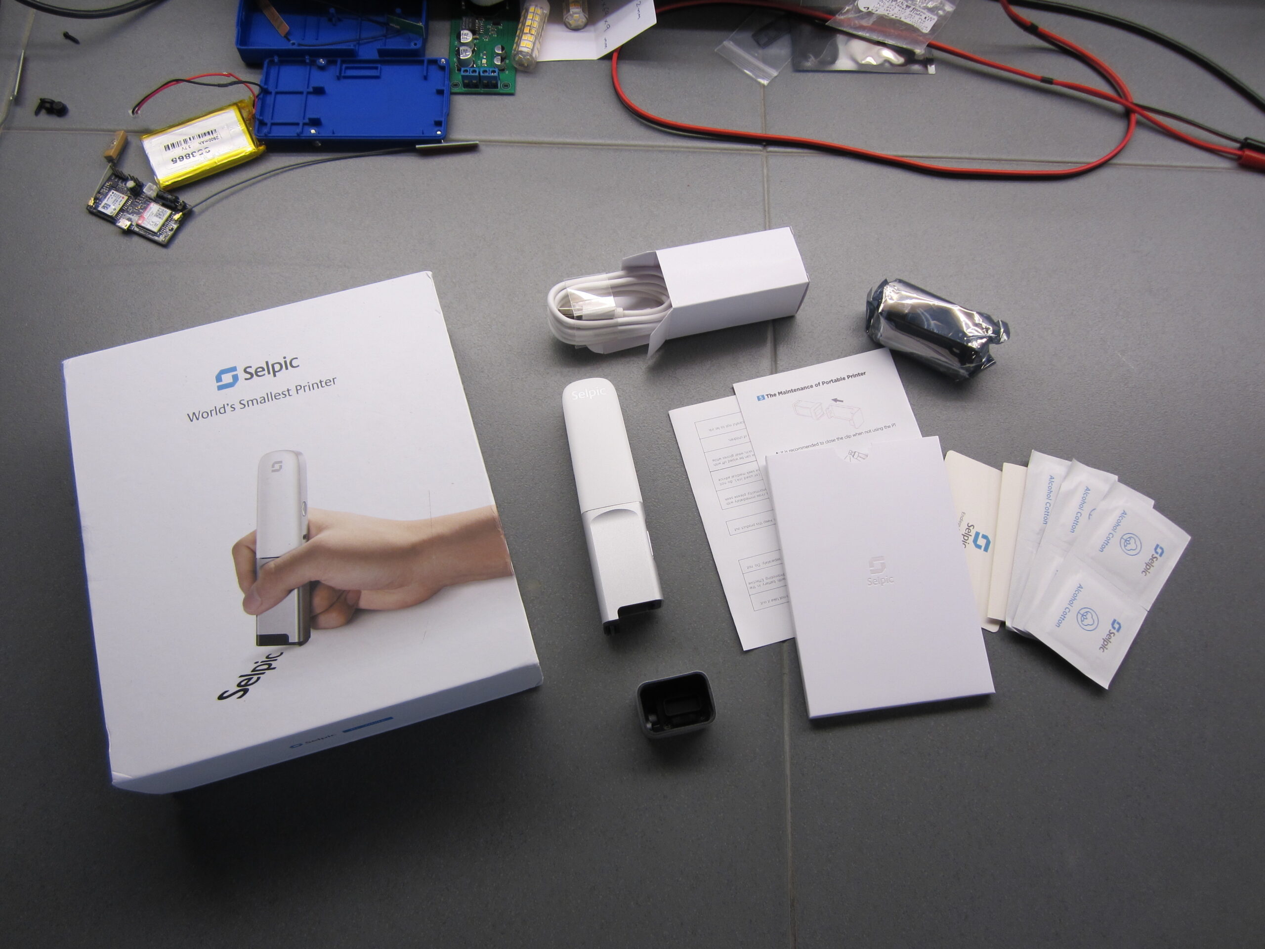
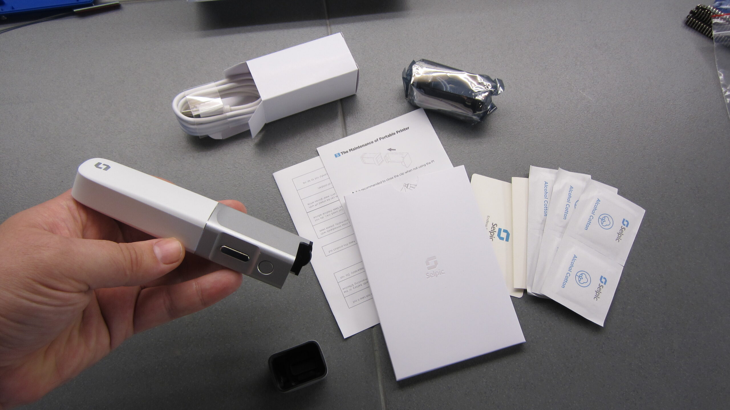
The printer comes in a good quality box that includes:
The handheld printer
1x ink cartridge
USB type C cable
Maintenance Manual
Alcohol wipes to clean the head
Guarantee Card etc.
Unboxing Video
Testing and Printing
To make your first print, you have to initially download the Android or iOS app from the appropriate app store. Launch the app to your smartphone and register for an account on Selpic if you haven’t already done it. The next step is to connect the Selpic P1 to your smartphone following the screen instructions. Once the connection is done, you will see the signal icon become light blue. Now you are ready to edit the text and icons using the inbuilt editor. We found the editor a little hard to use, because of the small icons and the not so self-explaining first three icons on the left side of the screen. You will need some time to familiarize your self with the app and when your artwork is ready you can click the far most right Print icon. The artwork is then transferred to the printer and you are ready to print. Grab the printer, hit the main button, and scroll it on the desired surface. Printing is started automatically as long as you scroll. Check the video above to see how this works.
Campaign
A campaign for the Selpic P1 is launcedh on INDIEGOGO with the device starting at only $99. There are several other packages planned with associated discounts. You can sign up to get notified for updates and also to get first option access to the diverse discounts like the super early bird discount of 55% off the $199 MSRP package which will be available to the first 500 backers.
While full-time embedded firmware developers like me may always have one thing or the other against the Arduino IDE, the truth is, the IDE remains one of the most versatile and widely used embedded development platforms in the world today. The success of the Arduino boards and related microcontrollers like the Atmega328p can be attributed to the versatility and ease of programming it brings, and one can easily link the success of more than 70% of microcontrollers/dev boards that have attained a level of popularity similar to the Arduino, to their compatibility with the Arduino IDE.
To benefit from the ease of programming offered by the Arduino IDE, communities around different microcontrollers build compatibility tools and one of the latest is the Sduino tool developed by Michael Mayor to facilitate programming of STM8 microcontrollers using the Arduino IDE.
The STM8 family of microcontrollers comprises the STM8S, STM8L, and STM8AF series of microcontrollers which are implemented around a high-performance 8-bit core and come with a state-of-the-art set of peripherals. They are manufactured using ST-proprietary 130 nm embedded non-volatile memory technology and support fast and safe development through enhanced stack pointer operations, advanced addressing modes, and new instructions.
The Sduino tool allows these microcontrollers to be programmed using the Arduino-C while and also supports the Standard Peripheral Library (SPL) which means the same code written on the Arduino IDE can be compiled with little or no modification on the official ST Visual Develop IDE.
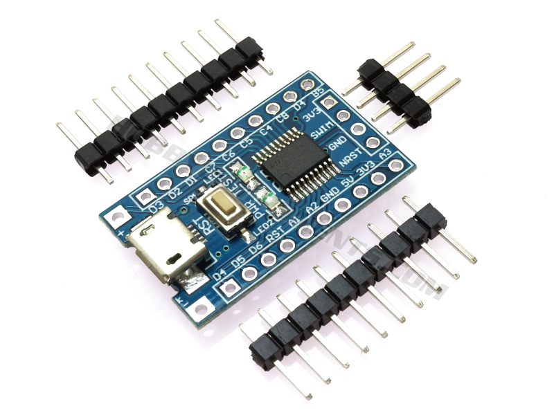
STM8S103F3 Development Board
Sduino is still under development and does not currently support a good number of popular Arduino libraries, but it supports enough to be useful. So for today’s tutorial, I will examine the process involved in setting up your Arduino IDE to program an STM8 based microcontroller. For demonstration purposes, we will use the STM8S103F Development Board, and our goal will be to upload the blink example to the board.
Ready? let’s go
Required Components
The following components are required to follow this tutorial:
The STM8S103F Development Board
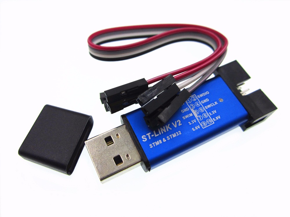
The ST link V2 programmer
A breadboard
Jumper wires
All of these components can be bought from your favorite electronics component store. We will use the LED onboard the STM8S103F development board, but if you will like to use a normal LED, you can add a LED and a 220 ohms current limiting resistor to the list of components.
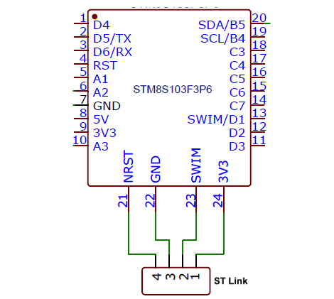
Schematics
Since we will implement the blink example using the LED onboard the STM8S103F, there is not much to do in terms of schematics. However, for those who may not be familiar with the process of connecting the ST link programmer to the STM8S103F board, the connection is described in the schematics below:
Schematics
For clarity, a pin map showing how the components are connected is provided below;
Go over the connections again to ensure everything is as it should be. If you are using the ST-Link for the first time, you will be required to install the driver and set things up. In most situations, driver installations will start automatically immediately you connect the ST-Link programmer to your computer.
ST-Link v2
Arduino IDE Setup
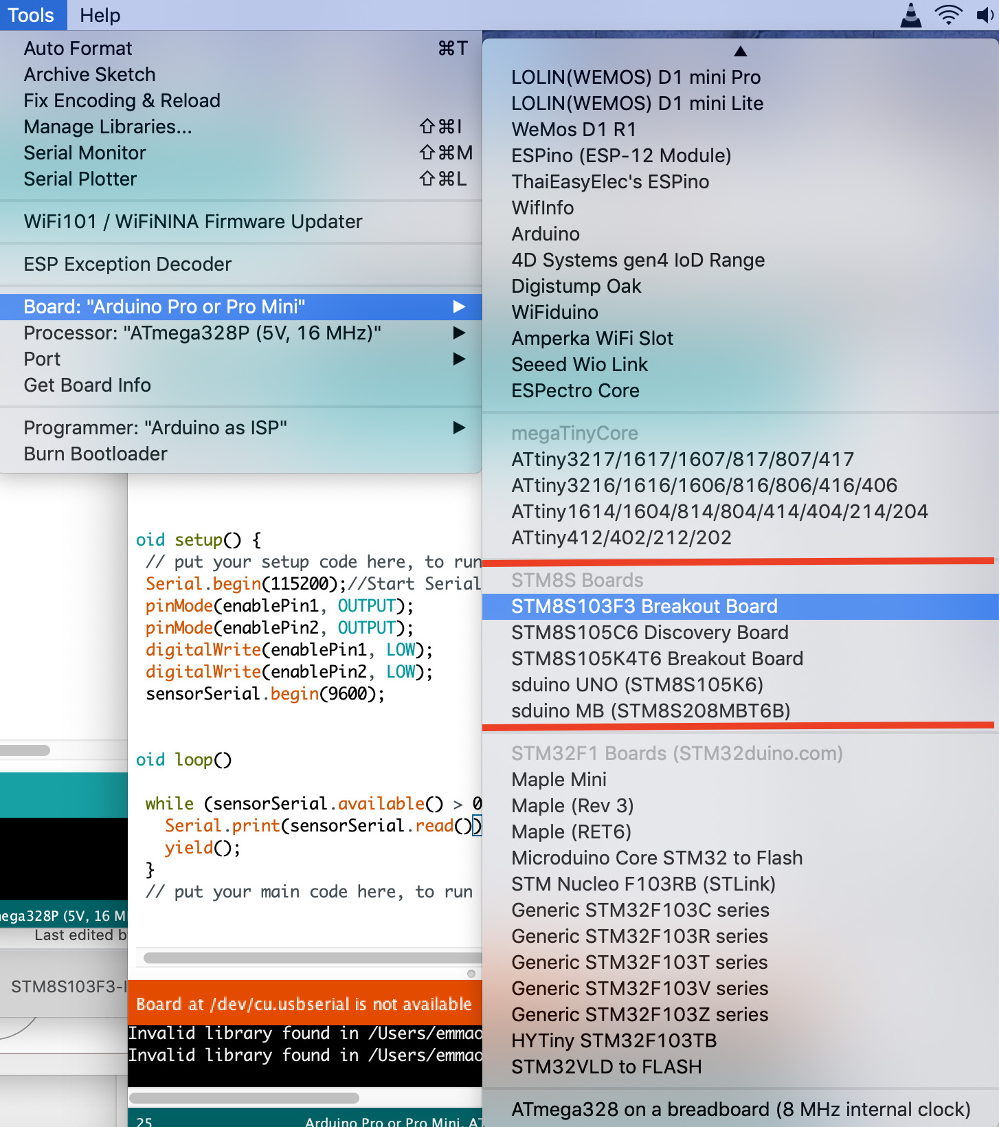
To make the process of integrating open-source boards with the Arduino IDE easier, the IDE comes with a feature called “board manager“. Through the board manager, new boards (essentially software-based components required for the Arduino IDE to be able to upload code to a particular MCU) can be added to the IDE. These software-based components, often called cores, are usually developed by manufacturers of the board (like Sparkfun does for its boards) or a group of users with the desire to see their board work with the Arduino IDE. The Sduino represents the core for the STM8s boards and we will be installing it on the Arduino IDE using the board manager. Follow the steps below to do this:
1. Open the preferences window from the Arduino IDE. Go to File > Preferences
2. On the preferences window, locate the “Additional Board Manager URLs” text box and enter this link; https://github.com/tenbaht/sduino/raw/master/package_sduino_stm8_index.json into the field as shown below. As you may have other URLs there already, separate the URLs from each other using a comma (“,”) and click OK when done.
3. Next, open the Arduino board manager. Go to tools>Boards>Boards manager
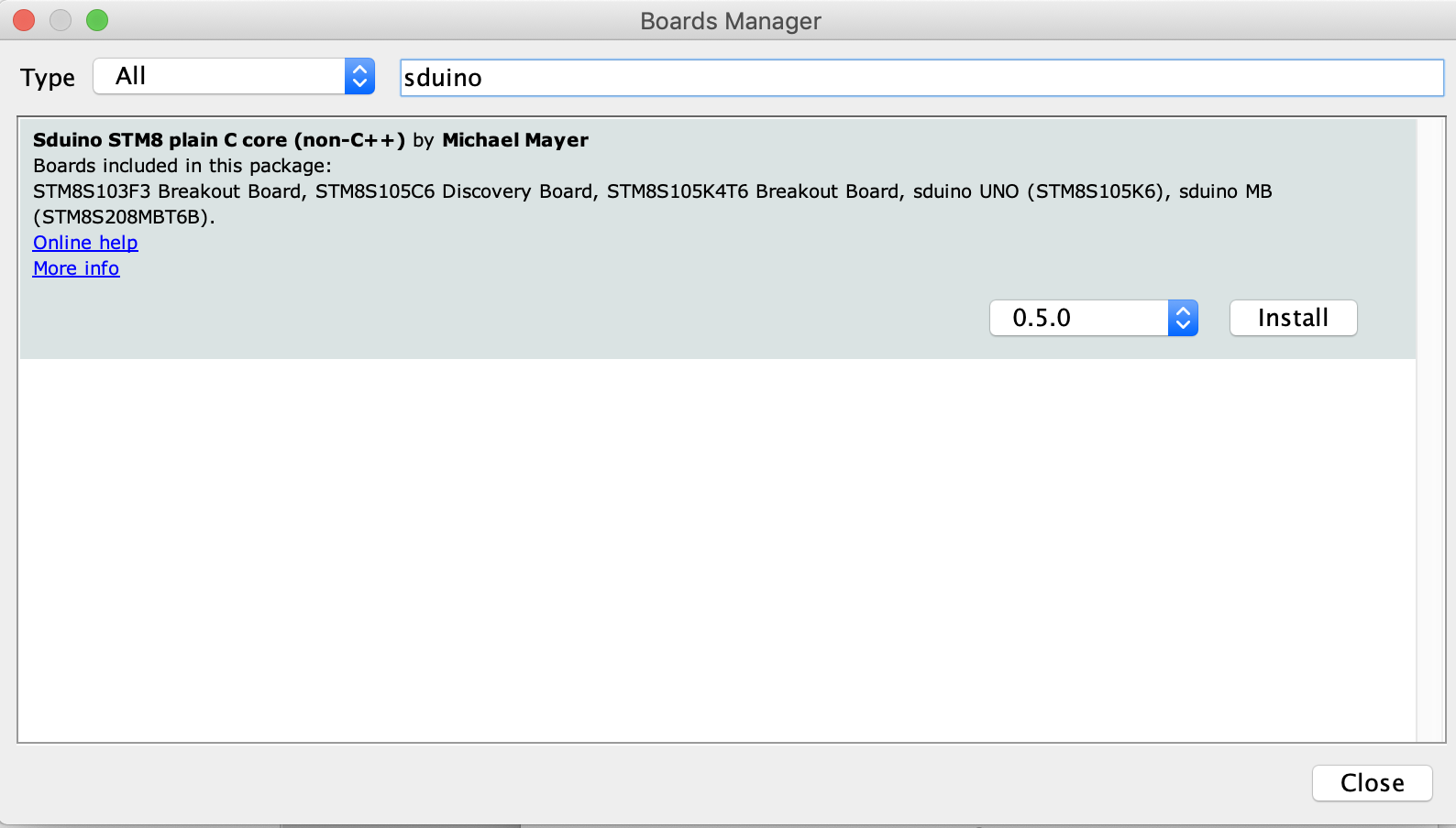
4. When the board manager opens up, enter Sduino into the search bar. You should see the Sduino core come up as shown in the image below. Click on the install button to install the core.
5. With the installation complete, close the board manager. The STM8s boards should now be available under the list of boards as shown in the image below.
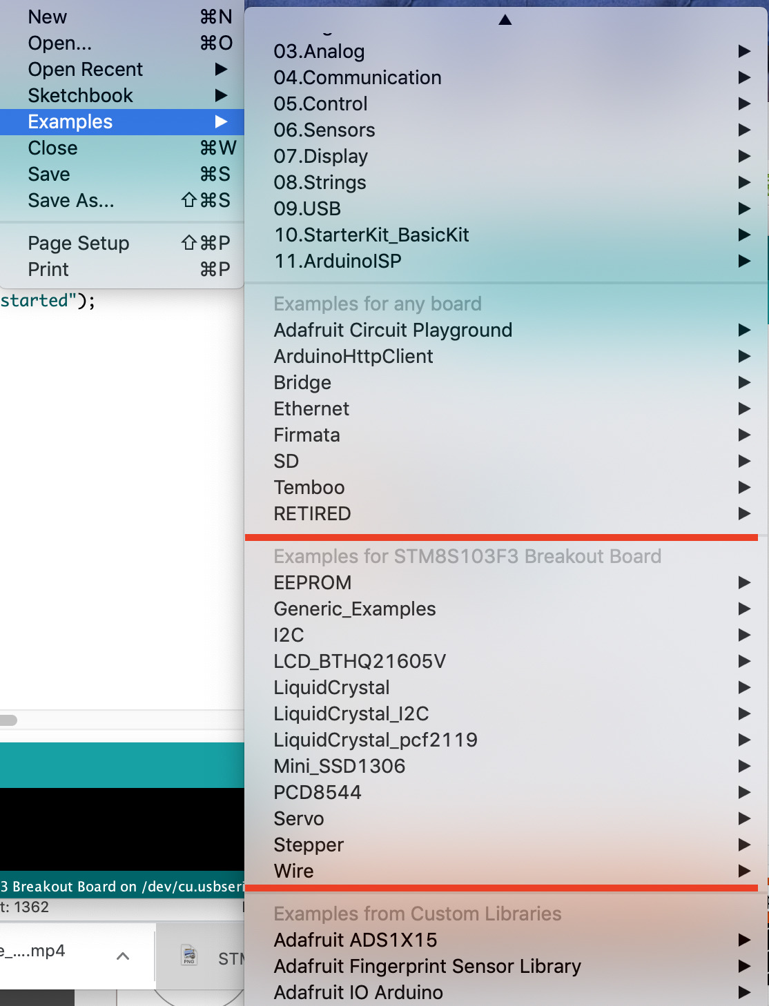
6. Installing the Sduino core will automatically install some Arduino libraries that have been modified to work with STM8s boards. Set your board type (by going to tools -> boards) to one of the STM8s boards, and go to examples (File -> examples). You will see a list of examples for the newly installed libraries.
With this done, you now have all you need to upload code to the STM8s boards.
Code
As mentioned during the introduction, for demonstration purposes, we will upload the blink example to the STM8S103F Development Board. You can use the generic blink example (File -> Example -> Basics -> Blink) or use the blink example among the STM8s Specific libraries (File -> Example -> Generic_Example -> Basics -> Blink).
I believe the code for the blink example needs no explanation and if you compare the two sketches you will see that they are exactly the same.
void setup() {
  // initialize digital pin LED_BUILTIN as an output.
  pinMode(LED_BUILTIN, OUTPUT);
}
// the loop function runs over and over again forever
void loop() {
  digitalWrite(LED_BUILTIN, HIGH);   // turn the LED on (HIGH is the voltage level)
  delay(1000);                       // wait for a second
  digitalWrite(LED_BUILTIN, LOW);    // turn the LED off by making the voltage LOW
  delay(1000);                       // wait for a second
}
Code Upload
Ensure your board is connected to the computer via the ST-link as described in the schematics. On the Arduino IDE, ensure the right board type is selected, and for set the programmer to ST-Link/V2 as shown in the image below:
With this done, hit the upload button, you should see the onboard LED begin to blink.
That’s it!
The Arduino IDE and Sduino provides a pathway to help you jumpstart development with STM8S. However, the platform is still under development and many Arduino libraries are yet to be supported.
That’s it for this tutorial! feel free to reach out to me via the comment section with questions or any clarifications you require.
Johanson Technology’s single antenna matching solution covers all relative frequency bands
Multiple frequency, protocol, and functionality solutions for IoT connectivity continue to push size and performance limits. To address this, Johanson Technology developed a multiband flexible solution using one antenna. This solution covers cellular (LTE), sub-GHz (868/915 MHz), GPS and/or GNSS (GLONASS), 2.4 GHz (Bluetooth® and/or Wi-Fi®) using one SMT chip antenna and two 6-channel RF switches. The entire solution requires a PCB area of about 360 mm, making it very compact with industry-accepted radiated gain and efficiency in a 51 mm x 51 mm board..
Features
Single antenna matching solution to cover all relative frequency bands
Can resonate at multiple frequencies
Requires antenna matching networks to cover cellular/sub-GHz/GPS-GNSS/2.4 GHz bands to achieve high efficiency and bandwidth
Entire solution requires a PCB area of about 360 mm, making it very compact with industry-accepted radiated gain and efficiency in 51 mm x 51 mm board
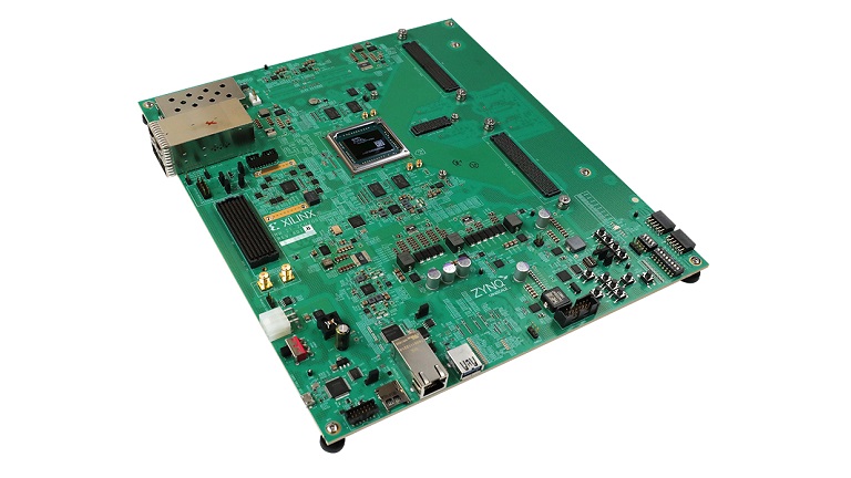
The Zynq® UltraScale+™ RFSoC ZCU208 Evaluation Kit is the ideal RF test platform for both out-of-box evaluation and cutting-edge application development.
The Xilinx Zynq UltraScale+ RFSoC ZCU208 ES1 Evaluation Kit features a Zynq UltraScale+ RFSoC ZU48DR, which integrates eight 14-bit 5GSPS ADCs, eight 14-bit 10GSPS DACs, and eight soft-decision forward error correction (SD-FEC) cores designed to jumpstart RF class applications. The combination of Arm® Cortex®-A53 and Cortex-R5 subsystems, UltraScale+ programmable logic, and the highest signal processing bandwidth in a Zynq UltraScale+ device, makes the ZCU208 evaluation kit the most comprehensive RF Analog-to-Digital signal chain prototyping platform.
Key features
Industry’s only single-chip adaptable radio platform
Zynq UltraScale+ RFSoC XCZU48DR-2FSVG1570E silicon featured on the ZCU208 Evaluation board
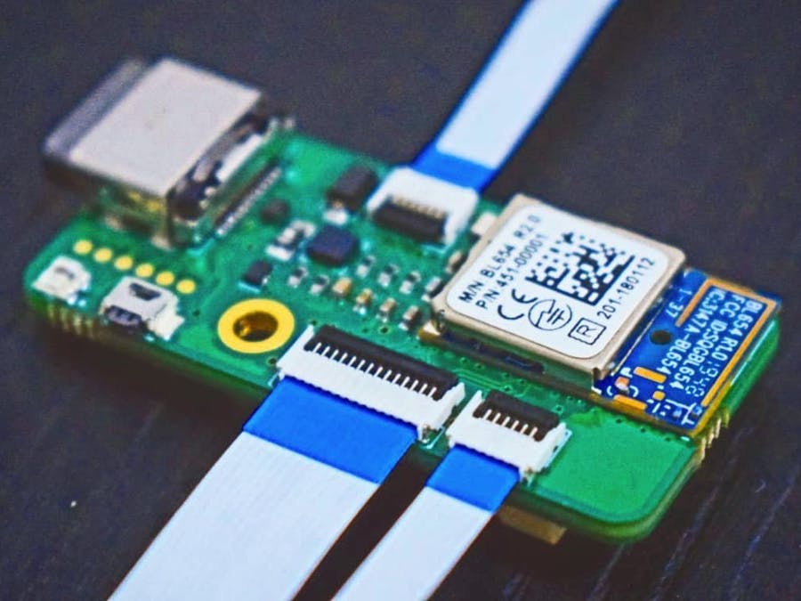
Covid-19 has inspired hundreds of health-related electronics projects from ventilators whose shortage was the initial worry for health professionals across the world to “basic” vital monitoring which was discovered to be very useful along the line. One of many projects which had remarkable engineering quality and huge potential in terms of application is the Life Data Link Monitor developed by team Horizon Medical comprising of hackster users; Jose Granados and Docomar01.
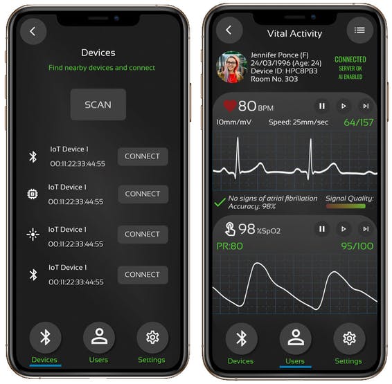
An open-source, low-cost, AI-enabled vital signs monitor designed to help manage the health status of COVID-19 patients, the Life Monitor was created to provide an innovative way for doctors to assess vital signs of thousands of patients via an AI-enabled IoT platform, to reduce the stress level of doctors and their contact with infected patients while ensuring the patients are monitored and get the best care possible.
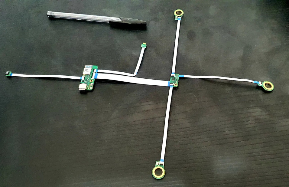
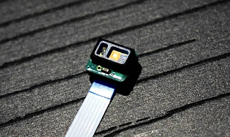
The Life Monitor makes use of up to 7 low-cost and small, wearable medical sensors that monitor parameters like; ECG, SpO2, Temperature,Heart Rate, Respiration Rate, accelerometer (activity and fall detection), estimated Blood Pressure, and pulmonary sounds and coughing (which is achieved via a lungs microphone). The device connects to a gateway which could be a phone, tablet, or a headless server via Bluetooth 5. The data is also securely transmitted to a cloud-based platform that leverages the power of the cloud and edge computing-based AI to draw inferences that help detect and manage worsening conditions of COVID patients.
Some features and specifications of the device include:
1 channel electrocardiography (ECG, also known as EKG) compatible with snap-type electrodes.
Respiration Rate (RR) measurement.
Photoplethysmography (PPG) and Oxygen Saturation (SpO2%) monitoring.
Temperature measure.
Activity and Fall detection.
Cough counting.
Systolic and Diastolic Blood Pressure Estimation (by firmware).
Rechargeable battery connector.
To facilitate easy development and configuration based on the needs of each patient, the project is totally modular, with the sensors connected to the mainboard via ribbon connectors, ensuring that all parts can be disassembled and assembled as needed. While a complete BOM is provided in the project documentation on hackster some of the main sensing elements used include:
ADS1292R for ECG and Respiration.
MAX30102 for PPG and SpO2.
TMP117 for ±0.1°C accurate temperature.
IIS2DLPC 3-axis accelerometer for activity and fall detection.
Dual ICS-43434 MEMS microphone
To ensure the timely response goals of the project was realized, the team also developed a companion app that makes it easy for doctors and caregivers to access the Life Monitor and get the vitals of patients.
As mentioned earlier, the project is completely open-source and everything required to replicate it, from schematics to Firmware and PCB designs are available on the Project’s Hackster page.
While it has become a norm for embedded firmware developers, tinkerers, and DIY electronics hobbyists to have multiple adapters for different communication protocols, the challenges associated with moving around with all the adapters can be quite the drag. The new Binho Nova Adapter is trying to change this by serving as a Multi-Protocol USB Host adapter, that allows users to connect I2C, SPI, 1-WIRE, and SWI devices (from sensors to microcontrollers, etc.) to computers over USB.
The device features 5 different signal pins, which in IO mode can be used varying functions like Digital Input, Digital Output, PWM Output, Digital Interrupt (on the rising edge, falling edge, or change), Analog Input, or Analog Output. Along with the 5 pins, then it also features a 3v3 pin, 1 VUSB pin, and 3 GND pins, all packed on a 10pin wire harness that terminates with a female 1.27mm 2×5 IDC connector.
Ideal for tasks like manual testing during firmware development, debugging, and automated hardware testing and validation. The pins on the Binho USB adapter can be used to communicate with any device on several digital buses like; I2C, SPI, UART, (Dallas)1-Wire, and (Atmel) Single-Wire Interface. While in the mode of operation that involves any of these protocols, the remaining pins, among the five(5), can be assigned to other related or unrelated purposes such as gpio, interrupts, chip selects, PWM signals, or analog input or outputs.
Some highlight features and specification of the adapter include:
Support for SPI @ 12MHz max clock
Support for I2C @ 3.4MHz max clock
Support for UART @ 1000000 max baud
Support for Dallas 1-Wire
Support for Atmel Single-Wire Interface
Provides 3v3 and VUSB power rails
1 x DAC Output, 5 x ADC Inputs
GPIO / Interrupt / PWM Support
Programmable RGB Status LED
Field-Upgradeable Device Firmware
Cross-platform Support for Windows, Mac, Linux
Robust, low-profile Aluminum Enclosure
USB Type-C Connector
A common use-case of the bingo adapter in production environments is for EEPROM/Flash Memory programming but it has also proven to be a lifesaver to users across related applications like;
Firmware Development
Proof of Concept Development
System Debugging
Automated Hardware Testing
Automated Firmware Testing
EEPROM Programming
FLASH Programming
FRAM Programming
The Adapter is currently available on Tindie for $149, and it ships in a package comprising a breadboard breakout adapter and a 1 foot USB type C (male) to type A (male) cable, all enclosed in a soft-shell zippered case.
More information on the product, price, and general availability can be obtained from the product’s page on Tindie.
Thermal imaging products company FLIR Systems has announced what it claims is the industry’s first thermal and visible sensor module for drone, robotic, and imaging manufacturers.
The FLIR Hadron dual sensor module for drone, robotic, and imaging original equipment manufacturers (OEMs) is designed to help reduce development costs and improve time to market. Offered in a lightweight (42.8 g), low-power, and 24 x 45 x 36-mm form factor, the device includes a 12-megapixel visible camera paired with the company’s Boson 320 x 240-resolution thermal camera with up to a 60-Hz frame rate.
“With the introduction of Hadron, FLIR Systems is leading the way in offering low-cost, dual sensor integration across a variety of industries from commercial drones to industrial imaging systems,” says Paul Clayton, General Manager, Components Business at FLIR. “Although our unmanned aerial system (UAS) customers are first to market with Hadron, this product empowers all of our OEM customers to increase performance with out-of-the-box functionality and simplified integration.”
In developing the Hadron, the company says it worked closely with drone manufacturers Vantage Robotics and Teal Drones to perfect the module for use on lightweight drone airframes. Vantage Robotics integrated the module into its micro-gimbal platform featuring its proprietary stabilization technology, offering a dual-sensor, OEM solution for existing UAS airframes and potentially other robotic platforms.
Tobin Fisher, CEO at Vantage Robotics says,
“Hadron is far and away the lightest and smallest combined visible-thermal sensor that has ever been commercially available. For an aircraft where you’re trying to push the limit on flight performance, every gram matters. The ability to get these sensor capabilities in a package this small makes an enormous difference.”
Teal has also integrated Hadron within its 2-lb (1 kilogram) Golden Eagle UAS platform, taking advantage of the module’s compact size to create a lightweight yet dynamic payload that helps preserve battery life and maximize flight time on a small airframe.
Teal Drones CEO and founder, George Matus says,
“Hadron enables us to speed development and time to market for small airframes with thermal and visual sensors. It’s high quality, low weight, and compact size allows for rapid integration to quickly develop prototypes.”
The project presented here is a photodiode amplifier for visible light. The output voltage of the circuit increases linearly with light intensity. Low-cost BPW34 photodiode is used as a light sensor and OPA381 op-amp as an amplifier. OPA381 is a transimpedance amplifier that converts photodiode current flow into voltage. The operating voltage of this circuit is 5V DC, and output ranges to almost 0V to 4.5V DC. The project can be used to make a LUX meter and other photo lab equipment. The analog output of the project is within the range of microcontroller’s ADC for easy interface with micro-controllers. By combining this project with Arduino and LCD, you can create a light meter for photography. It is advisable to use filters in front of the sensor to stop infra-red noise as the sensitivity of BPW34 is near to infrared. Half-cut table tennis ball will help as a filter.
Photodiode Amplifier for Visible Light Using OPA381 – Arduino Nano Shield – [Link]
Diodes Incorporated announces the AP64350Q/AP64351Q/AP64352Q series of automotive-compliant, 3.5A, synchronous buck converters for point of load (POL) applications.
Diodes Incorporated today announced the AP64350Q/AP64351Q/AP64352Q series of automotive-compliant, 3.5A, synchronous buck converters for point of load (POL) applications. The AP6435xQ combines a low quiescent current with a wide input voltage range of 3.8V to 40V. The devices have been developed for use in automotive applications including infotainment systems, instrument clusters, telematics, advanced driver assistance systems (ADAS), and forward lighting.
With a fully integrated 75mΩ high-side power MOSFET and 45mΩ low-side power MOSFET, AP6435xQ provides high-efficiency step-down DC-DC conversion. The design of the AP6435xQ’s gate drive/bootstrap enables the devices to operate in low drop out (LDO) mode, allowing near 100% duty cycle.
To increase efficiency as the load current approaches zero, the devices enter pulse frequency modulation (PFM), resulting in a quiescent current of just 22μA. They also feature frequency spread spectrum (FSS) with a switching frequency jitter of ±6% and a proprietary gate driver scheme, which reduces high frequency radiated EMI noise caused by MOSFET switching.
The AP64350Q, AP64351Q, and AP64352Q have distinct additional feature sets that optimize performance in slightly different ways. The AP64350Q and AP64352Q have an adjustable switching frequency (100kHz – 2.2MHz) and can also be synchronized to an external clock. This provides the design flexibility to deliver a choice of low frequency with extremely high efficiency, or high frequency for small form factor solutions whose switching frequency is outside the AM band. The AP64351Q and AP64352Q have programmable soft-start, which reduces in-rush currents, while the AP64350Q and AP64351Q have external compensation to optimize loop response.
The AP64350Q, AP64351Q, and AP64352Q are qualified to AEC-Q100 Grade 1, support PPAP documentation, and are manufactured in IATF 16949 certified facilities. The devices are available in the SO-8EP package priced at $0.93 in 1000 piece quantities.
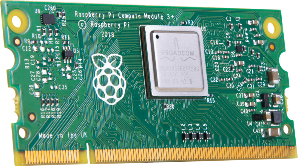
The launch of every new revision/version of Raspberry Pi Board has always been followed with the release of the Raspberry Pi Compute Module based on that version. Things will not be different with the recently released Raspberry Pi 4, as the CEO of Raspberry Pi Trading, Eben Upton, in a recent interview, shared some plans to release the Raspberry Pi 4 Compute Module in 2021.
Speaking on the popular weekly Raspberry Pi-Centric Show by Tom’s Hardware, Pi Cast, Eben talked about plans to release the Compute Module board within the next year, while affirming plans to incorporate some of the features that the community has clamored for since the launch of the Pi 4. In his words,
“The Raspberry Pi Compute Module, CM4, we will support NVMe to some degree on that, because of course, it [Raspberry Pi 4] has a PCI Express channel,”. Sharing more light on how this will be achieved, he said ” we have a single lane Gen 2 which is used to supply USB 3 on the Raspberry Pi [4]. On the [Compute] Module that would be exposed to the edge connector and we’re likely to support NVMe over that.”
One of the great things about the Raspberry Pi 4 is the onboard processor; the Broadcom BCM2711, which among several other things, comes with a PCIe interface that would have allowed users to directly connect storage devices and attain data transfer rates greater than the Max 40MBps that is possible with MicroSD cards. However, the interface was not exposed on the board as it was being used by the VL805 PCIe USB 3.0 controller for the USB ports, and why a lot of users have been able to hack their way around it, having it exposed on the compute module means there’s a ray of hope for users without the hacking skills.
Raspberry Pi Compute Module 3+
Since the Compute Module comes with no ports and other features possessed by the regular Model B boards, the availability of this PCIe interface will only be useful to Industrial users for which the compute module was created. As such, Eben was asked the possibility of the PCIe interface being exposed to a traditional model B version of the board. His answers were affirmative, but he noted that it will require a lot of design modifications that may impact the cost, and size of the board.
Speaking further on the next steps with the Pi 4, Eben acknowledges the possibility of a Model A version of the board which he said might be the regular board version with the PCIe exposed, but he mentioned the challenges of keeping the price within the same range as the Model B.
Several other tips on what to expect from the Raspberry Pi team was shared on the show. You can watch the episode on YouTube to find out more about all that was discussed.