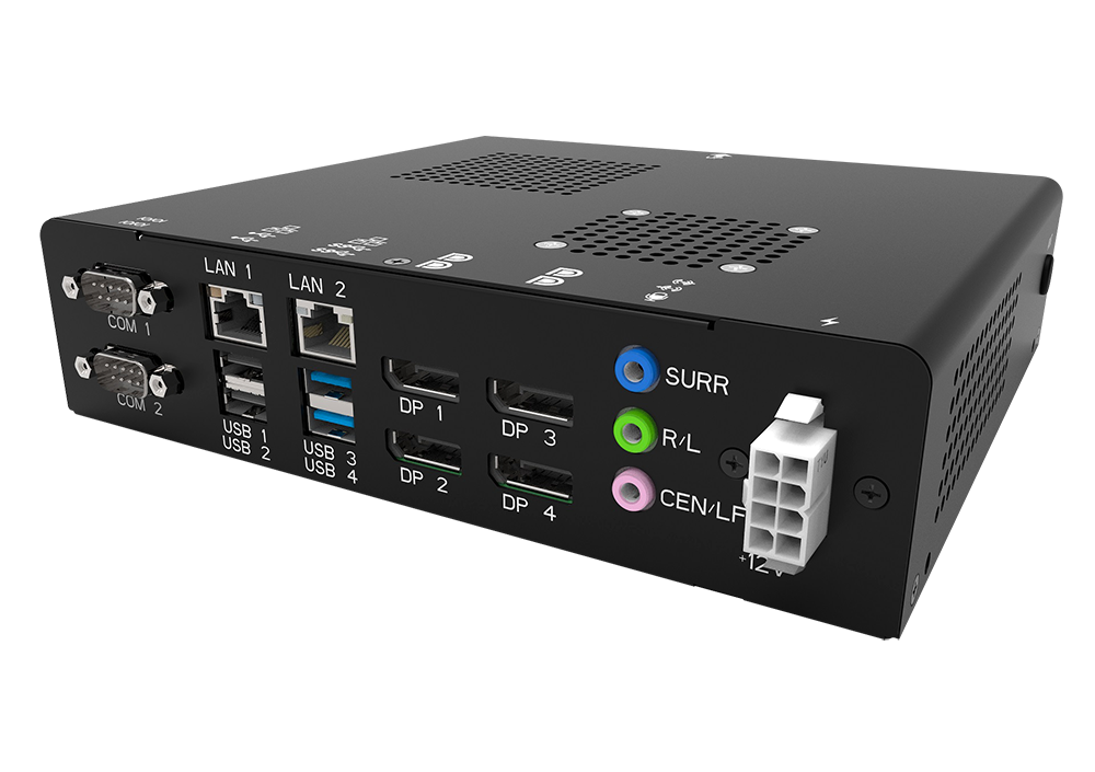
EFCO, a world-class supplier of industrial computers and gaming and EMS solutions, today announced VideoStar100, the first media player integrated with SecuBoot™ to provide the most advanced security available for digital displays. Equipped with an AMD industrial-grade Ryzen™ Embedded V1000/R1000 APU, VideoStar100 provides the performance to support three (R1000) or four independent 4k displays and can be used for applications ranging from slot machines to digital display walls, especially for those displays used to introduce the games.
“We wanted to give our customers the most secure, yet cost-effective, solution to play 4K digital display content. Because VideoStar100 is equipped with SecuBoot™, this media player is uniquely able to provide the same level of security for your content as is required on today’s casino gaming floors,” Ira Lo, CTO for EFCO commented. “We are the first company to bring this level of security to a media player, and it also provides high performance applications with support for up to four independent 4k displays.”
About SecuBoot™
Security is a priority for VideoStar100 and the integrated SecuBoot™ ensures that a trusted game environment is operating by preventing malicious applications. This prevents “unauthorized” programs or viruses from USB devices or from Internet hackers to change the operating system during the system start-up process. EFCO SecureBoot™ provides a complete algorithm to cover BIOS Lock, Device Verification, Storage Checksum, and Whisper Talk, which meets country and/ or regional regulations. By including this extra level of security, SecuBoot™ also aids in the ability to meet the requirements of GLI or BMM.
About VideoStar100
VideoStar100 is a high performance, cost-effective 4K media player for the digital signage market. Based on the AMD Ryzen™ Embedded V1000/R1000 Series, it has integrated SecuBoot,™ to provide advanced protection for your content. VideoStar100 supports up to 4 independent displays with an integrated AMD Radeon™ Vega Series Graphic Processor. Other features include optional SmartBay,™ which supports SATA storage and USB2.0/3.0 ; up to 4 DP ports; 2 RS232 ports, 2 RJ45 ports and supports VESA Mount. Lifetime support until 2028 is also included.
Availability
VideoStar100 is available now. For more information, contact info@efcotec.com.
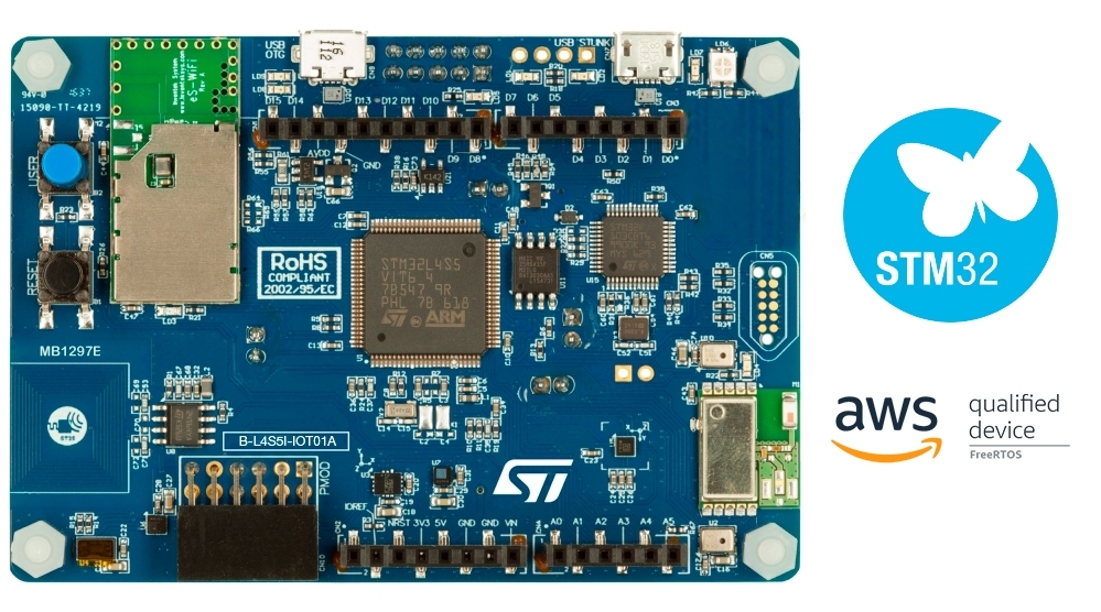
With the B-L4S5I-IOT01A Discovery kit for IoT node, users develop applications with a direct connection to cloud servers. The Discovery kit enables a wide diversity of applications by exploiting low-power communication, multiway sensing and Arm® Cortex®-M4 core-based STM32L4+ Series features. The support for ARDUINO® Uno V3 and Pmod™ connectivity provides unlimited expansion capabilities with a large choice of specialized add-on boards.
Key Features
Ultra-low-power STM32L4+ Series STM32L4S5VIT6 microcontroller based on the Arm® Cortex®-M4 core with 2 Mbytes of Flash memory and 640 Kbytes of RAM in LQFP100 package
64-Mbit Quad-SPI Flash memory from Macronix™
Bluetooth® 4.1 module (SPBTLE-RF) from STMicroelectronics
802.11 b/g/n compliant Wi-Fi® module (ISM43362-M3G-L44) from Inventek Systems
Dynamic NFC tag based on ST25DV04K with its printed NFC antenna
2 digital omnidirectional microphones (MP34DT01) from STMicroelectronics
Capacitive digital sensor for relative humidity and temperature (HTS221) from STMicroelectronics
High-performance 3-axis magnetometer (LIS3MDL) from STMicroelectronics
3D accelerometer and 3D gyroscope (LSM6DSL) from STMicroelectronics
260-1260 hPa absolute digital output barometer (LPS22HB) from STMicroelectronics
Time-of-flight and gesture-detection sensor (VL53L0X) from STMicroelectronics
Highly-secure solution (STSAFE-A110) from STMicroelectronics
2 push-buttons (user and reset)
USB OTG FS with Micro-AB connector
ARDUINO® Uno V3 expansion connector
Pmod™ expansion connector
Flexible power-supply options: ST-LINK, USB VBUS or external sources
On-board ST-LINK/V2-1 debugger/programmer with USB re-enumeration capability: mass storage, Virtual COM port, and debug port
Comprehensive free software libraries and examples available with the STM32Cube MCU Package
Support of a wide choice of Integrated Development Environments (IDEs) including IAR™, Keil®, and STM32CubeIDE
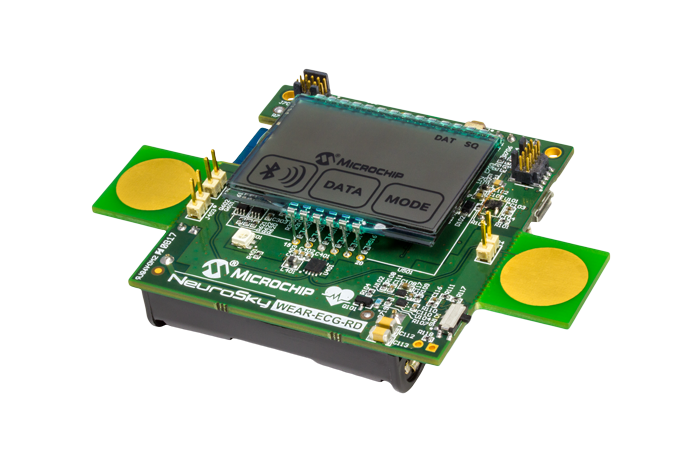
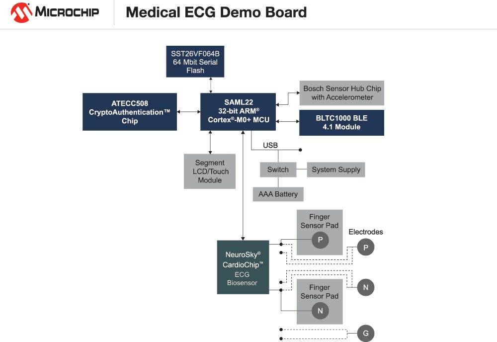
Microchip’s innovative design for portable and accurate ECG heart monitoring applications
The electrocardiogram or ECG machine design from Microchip Technology is used to monitor and record the electrical activity of the heart. This design features the SAML22, a high-performance, 32-bit Arm® Cortex®-M0+ microcontroller with ultra-low-power technology, the BTLC1000 Bluetooth® Low Energy (BLE) 4.1 module, the ECC508A Crypto Authentication chip, and the NeuroSky® CardioChip™ ECG biosensor. Since each heartbeat produces an electrical impulse in the heart, the generated cardiac electrical potentials can be measured with sensors placed on the body at different locations. Abnormal electrical activity can indicate conditions such as heart attack, chest trauma, reduced blood flow to the heart, arrhythmia, or heart deformities. The ECG demo measures a complex heart rate and computes other heart-related data. Patient movement is also tracked via an on-board accelerometer. The BTLC1000 BLE module on this board allows the demo to communicate with tablets, smartphones, or PCs for IoT capability.
The demand for portable and accurate ECG monitoring has grown substantially. Despite the smaller size of these portable products, ECG devices still require precision filtering, high-performance processing power, and integrated high-resolution graphics control that is separate from the main microcontroller core. As medical remote patient monitoring becomes more important, the need for wearable ECG capability has become critical. Microchip’s Connected, Wearable ECG Demonstration Board can be used in the design of advanced fitness tracking devices and can also be designed into medical wearable remote patient monitoring and diagnostic systems.
Features
Ideal for portable/wearable medical/fitness designs
Measures heart rate and computes heart rate variability, heart age, and stress using ECG data
Easy development of more advanced heart-healthy index functions
Demo can also be shown using standard ECG leads
BLE module is used for smartphone/tablet IoT capability
Low overall BOM cost due to high level of integration
TDK-Micronas‘ HAL1880 is an entry-level Hall-effect sensor with ratiometric analog output, offering the best compromise related to sensor function vs system cost. It includes programmable clamping to extend error signaling capability and diagnostics associated with the state of various internal circuits (magnetic signal out of range). A one-pin programming interface enables the simultaneous programming of several devices through the output pin.
The HAL1880 is a programmable sensor: major characteristics like magnetic field range, sensitivity, offset, and the temperature coefficients are programmable in nonvolatile memory. The sensor is designed for industrial and automotive applications, is AEC-Q100 qualified, and operates in the junction temperature range from -40°C up to +170°C. It is available in the very small leaded package TO92UA.
Features
Overvoltage and reverse-voltage protection at VSUP pin
Measurement ranges from ±20 mT to ±160 mT
Short-circuit protected push-pull output
5 V supply operation
Selectable sampling rate
TJ = -40°C to +170°C
AEC-Q100 qualified
Benefits
Programmable temperature characteristics for matching all common magnetic materials
Programming via output pin or supply voltage modulation
Operates with static and dynamic magnetic fields up to 5 kHz
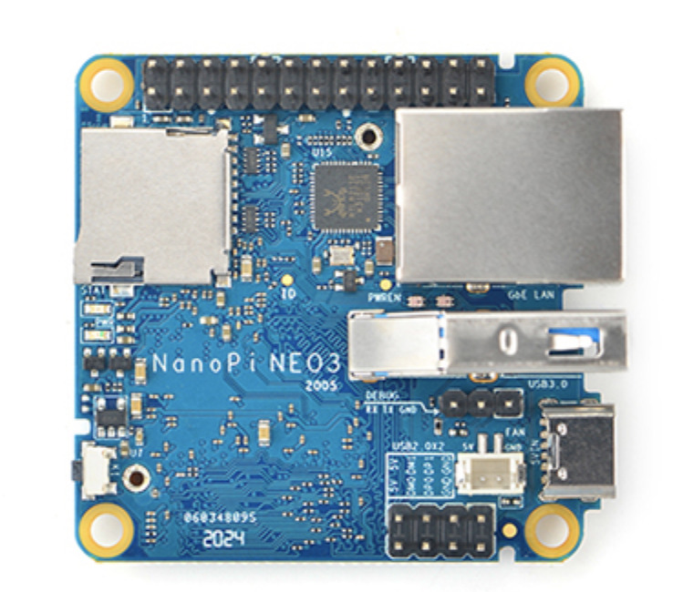
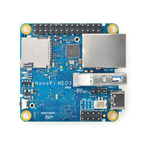
The recently launched NanoPi Neo3 from FriendlyElec is a single board computer that runs Linux on a quad-core Cortex-A53 Rockchip RK3328 and has 1 or 2GB DDR4, Gigabit Ethernet port, USB 3.0, and a wide operating range of -20 0C to 70 0C. Like most of the earlier released Neo models from FriendlyElec, the new Neo3 SBC is a headless board with a compact footprint measuring 48 mm by 48 mm.
The company had earlier announced its Rockchip RK3399 based NanoPi Neo4 single-board computer that came with a lot of excitement as the first SBC to break RK3399 records for size and price, measuring 60 mm by 45 mm with a starting price of $45 and above.
While the NanoPi Neo3 offers a similar but less powerful RK3328 Rockchip SoC as the Neo4, the Neo3 offers both 1GB and 2GB of DDR4 unlike the 1GB of DDR3 available on the Neo4, and also starting at a $20 price tag compared to the $45 start price for the Neo4.
Some highlight features and specifications of the NanoPi Neo3 SBC include:
CPU – Rockchip RK3328 Quad Cortex-A53 cores clocked to 1.5 GHz with a Mali-450 MP2 GPU
1 GB or 2 GB DDR4 RAM
Gigabit Ethernet port with unique MAC address
Bootable MicroSD slot
26-pin GPIO header
2x USB 2.0 headers and USB 3.0 host port
Serial debug header
Fan connector
Micro USB power for power input only (5V)
2x LEDs
1x user key
5V/1A DC via GPIO or Type-C
Temperature Range: -20 – 70 0C
Operating Systems: FriendlyWrt and Ubuntu Core 18.04
Weight- 22 grams
Dimensions – 48 mm x 48 mm
The cheap price of the NanoPi Neo3 puts it in the same category has other open-spec, community-backed RK3328 SBCs like Firefly’s $35 ROC-RK3328-CC and Pine64’s $25 Rock64 SBC. However, even though the price of the Neo3 also goes up with an increase in RAM, the increase is not at an exponential rate like that of the other boards, as the 2Gb ram version of the Neo3 costs only $25.
All round, the Neo3 is a noteworthy SBC and the only shortcoming I feel it has is the lack of media interfaces and a few other features that one might expect from a hacker board.
As mentioned earlier, the NanoPi Neo3 SBC with 1GB RAM goes for $20, while the 2 GB RAM version is being sold for $25. Irrespective of the version you go with, you can also add accessories like; a heatsink case that goes for an additional cost of $2, optional power adapters, cables, and a USB-based LCD module for Pi.
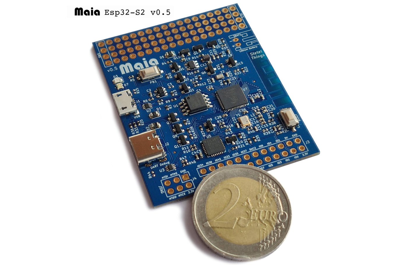
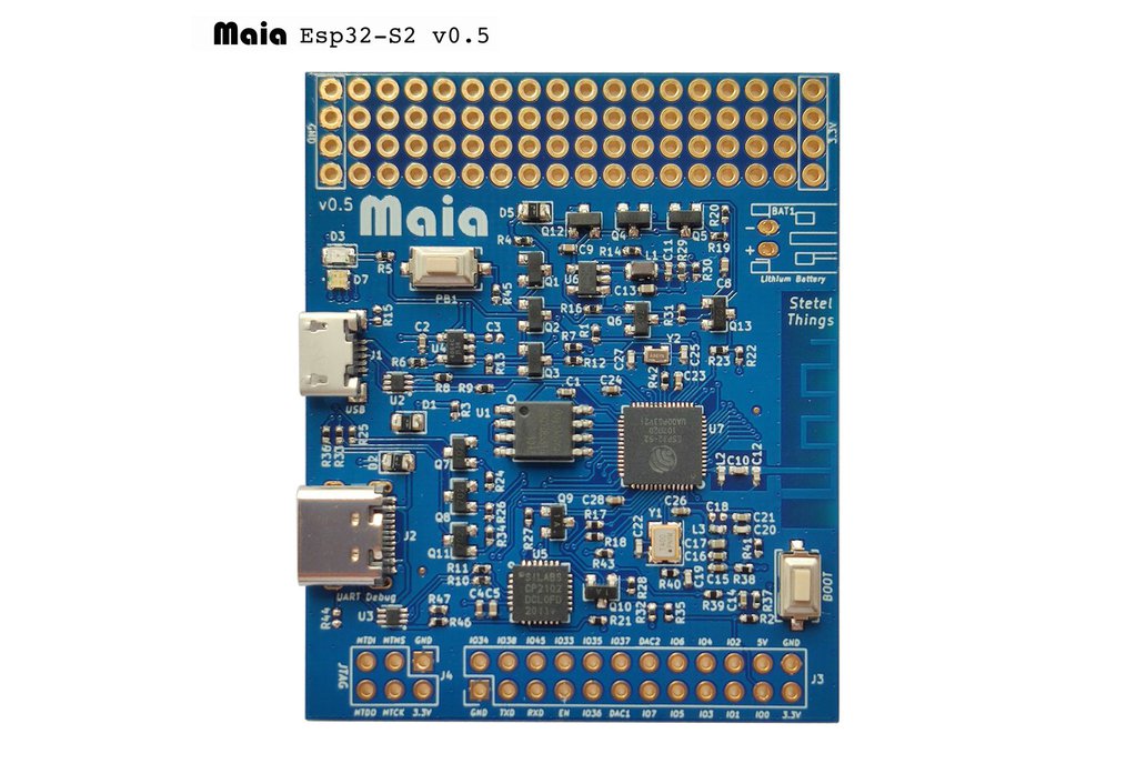
So far so good, only a few boards have been able to take advantage of the extra USB OTG interface offered by the ESP32-S2 processor released back in 2019, and one of them is the new Maia development board from Stetel Things.
As a quick reminder, the ESP32-S2 was unveiled with quite some incredible features like a primary 240 MHz Xtensa LX7 processor, a RISC-V based ultra-low power coprocessor (free and open-source), an in-built USB OTG interface, WiFi, a camera interface and several hardware security features amongst others.
The new Maia development board by the Italy-based Stetel Things offers an easy platform for makers to develop, play, and build USB and IoT devices. The board comes with an interesting layout that comprises of the Espressif ESP32-S2 microcontroller, a micro USB OTG port which sits next to a typical USB Type-C port for power and debugging, and a small area that can be used for prototyping.
The Maia development board is perfect for many ESP32-S2 projects from Portable Secure IoT applications and USB OTG devices, to RISC-V development with a second ULP.
Weighing 13.6 grams with dimensions of 5.9 cm by 4.9 cm, the Maia comes at a fair size for the features it embodies. Some of the key features and specifications include;
Espressif System ESP32-S2 single-core LX7 running @ 240 Mz with a RISC-V ultra-low power CPU
320KB RAM and 4MB flash
1x USB-C for programming and 1x micro USB OTG port for data (both ports can be used as power input)
802.11b/g/n WiFi 4 with integrated PCB antenna
Programmable user button that can also function as the Power button
Boot button
RGB LED, Charging/power LED
RTC clock
6-pin 2.54mm pitch JTAG header
24-pin I/O header
Playground Prototyping area with 4x 18 through holes for user applications
5V power supply through the USB Type-C or micro USB
3.7V Li-Po battery with a 2-pin battery connector and an integrated Lithium battery charger IC
The Maia development board like most ESP32-based boards is quite flexible and can be programmed with Arduino, ESP-IDF SDK, MicroPython, and ESP RainMaker.
Source code for firmware as well as instructions for the ESP RAINMAKER and DFU web flasher are all available on Stetel Things’ GitHub repository while the board itself can be purchased for $19.70 on Tindle.
A plastic enclosure kit with micro USB port, light guides for RGB and charging LED, power button and lithium battery is also in the works, but currently not available for sale.
We have seen in the previous tutorial about Voltage Dividers and that the voltage division process is made possible by associating the same components in a series configuration. In this article, we will focus on the current division process performed by Current Dividers which are parallel associations of components.
The most common type of current divider is discussed in the first section, in its simplest form, it consists of two resistors in parallel.
Some more configurations and details about the resistive current dividers are examined in the second section.
Finally, alternative forms of current dividers partially made with reactive components are presented in the following sections.
Presentation
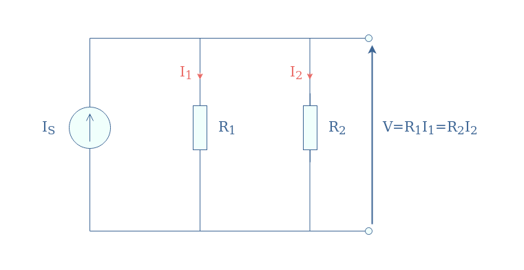
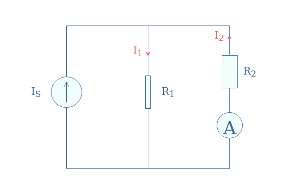
The most basic resistive current divider configuration is presented in Figure 1 below:
fig 1: Illustration of a resistive current divider
We will now demonstrate the current divider formulas, that is to say, the expressions of I1 and I2 as a function of the source IS and the resistances R1 and R2.
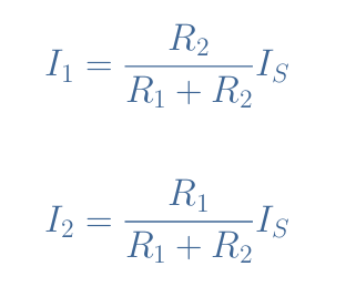
First of all, we express both currents as a function of the voltage V thanks to Ohm’s law: I1=V/R1 and I2=V/R2.
According to Kirchoff’s current law, the current source can be written as the sum of the independent current in each branch: IS=I1+I2=V×(1/R1+1/R2).
Under the same denominator, this expression becomes V=(R1×R2/(R1+R2))×IS. Finally, we replace V in the expressions of I1 and I2 to obtain the resistive current divider formulas:
eq 1: Resistive current divider relations
The dimensionless factors in these expressions range from 0 (R2=0 in the expression of I1 or R1=0 for I2) to 1 (R1=0 for I1 and R2=0 for I2) which is interesting to get any possible value of output current from 0 to IS by setting proper values for the resistors.
In practice, the resistance values are never equal to 0 for the simple fact that the resistance of the wires is small but not zero. However, we can still say that for R1>>R2, I1=0 and I2=IS, and for R2>>R1, I1=IS and I2=0.
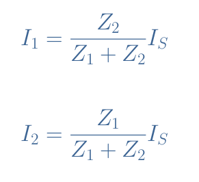
The expressions of Equation 1 can be generalized for any component that constitutes the current dividers, for this, we use the impedance formalization:
eq 2: General current divider relations
Since current dividers consist of associations of components in parallel, it is often recommended to use admittances instead of impedances in order to simplify calculations. Indeed, the admittance of a resistor R is written Y=1/R, and in a parallel configuration, the admittances are simply added up: Ytot=Y1+Y2+…
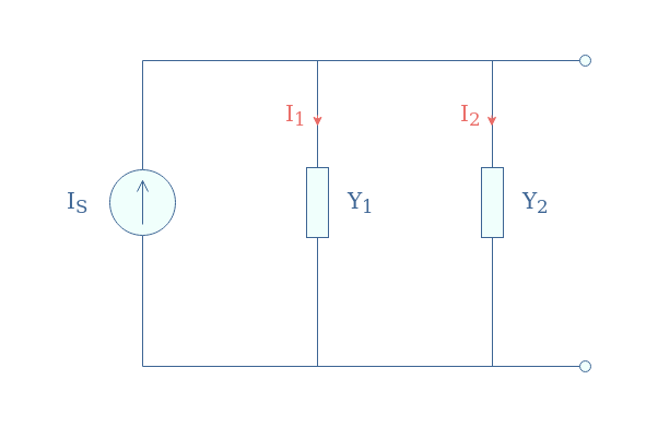
To illustrate the simplification improvements of this method, we reconsider the circuit in Figure 1 with the admittances:
fig 2: Resistive current divider with the admittance notation
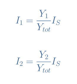
Here, the equivalent parallel admittance is simply given by Ytot=Y1+Y2. Therefore, we have the relation V×Ytot=IS. When replacing V in the expression I1=V/R1=V×Y1 and I2=V/R2=V×Y2, we get the following relations:
eq 3: Admittance form of the resistive current divider relations
A very useful application of current dividers is to safely measure currents while protecting the measuring instrument and user. An example of a current measure is given in the following Figure 3:
fig 3: Process to safely measure a high DC current
The shape of the components accounts for the proportions that the resistors should take. Indeed, in order to protect the amp meter of high currents, the resistor R2 must be higher than R1 to limit the current across the measuring device.
As an example, if the source provides a current IS=1 A but the amp meter accepts a maximum of 0.05 A, we can choose values for R1 and R2 so that the ratio R1/(R1+R2) is equal or lower than 1/20. The values R1=1 kΩ and R2=19 kΩ would for example satisfy this condition.
Finally, in order to display the correct value to the user, the amp meter simply proceeds to multiplicate the measurement value by the inverse fraction (R1+R2)/R1.
General/network configuration
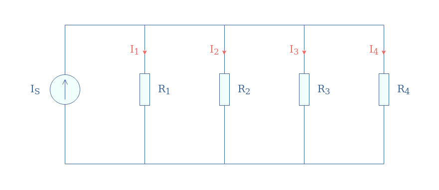
A general or network current divider configuration is made with more than two resistors in parallel. In the following Figure 4, we illustrate a resistive network current divider with 4 components:
fig 4: Illustration of a resistive current divider network
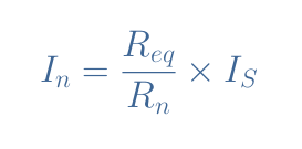
For such a circuit or for any current network divider composed of N resistors, the general formula for any current is given by Equation 4, with Req being the parallel equivalent resistance value.
eq 4: Currents expressions in a current divider network
A current divider network can be used to limit the current in the output, such as presented with the amp meter in Figure 3, but moreover to limit the current in each individual resistor.
As an example, if we reconsider the configuration given in Figure 3 we can compute the power dissipated in each resistor:
P1=R1×I12=1000×(0.95)2=903 W
P2=R2×I22=19×103×(0.05)2=47 W
The value of 900 W in the resistor R1 is clearly too much to handle and would melt the resistor structure, even with specially designed high-power application resistors.
With a current divider network, we can split the total amount of power (1000 W) more equally and with lower values in each resistor. We could choose for example to associate 20 resistors in parallel of the same values (1 kΩ). In this case, each resistor would only absorb 0.05 A and dissipate a low-value of 1000×(0.05)2=2.5 W, which respects both conditions of resistors and measuring device protections.
Reactive current dividers
When considering Figure 2, we can replace one of the admittances (say Y2) by a reactive component such as a capacitor or an inductor. These possible associations give interesting properties in the AC regime to the current divider.
Resistor-capacitor current divider
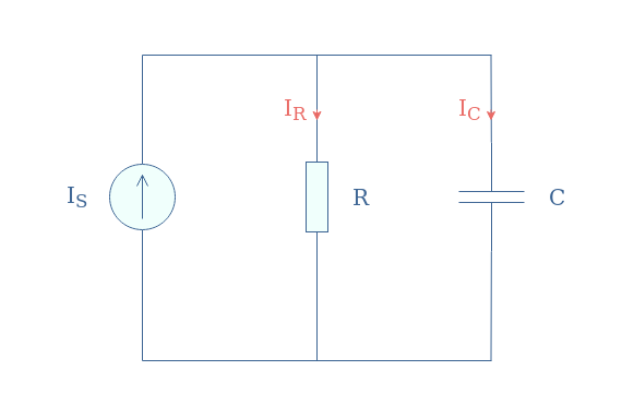
In this configuration, a resistor is placed in parallel with a capacitor such as presented in Figure 5. We refer to this current divider as an R//C association.
fig 5: R//C circuit association
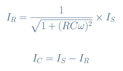
It can be shown that the current across the resistor and capacitor are frequency-dependent and can be expressed by the following relations shown in Equation 5. The current expression of IR is obtained by the generalized current divider formula and the expression of IC by simply applying Kirchoff’s current law.
eq 5: Current expressions in an R//C association
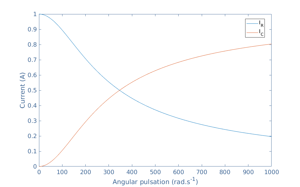
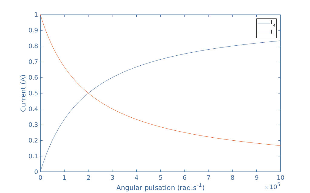
We choose R=1 kΩ, C=5 μF, and IS=1 A in order to show a plot example of these currents:
fig 6: Currents plots IR(ω) and IC(ω) in an R//C association
As we can see, due to the reactance of the capacitor, the current IC is zero for low frequencies and increases up to a short-circuit for high-frequencies. On the other hand, the resistor current decreases when the source frequency increases. Note that IR+IC is a constant and equal to IS=1 A.
In practice, R//C circuits are used as low-pass filters in order to cut high frequencies at the output. Moreover, a parallel capacitor is often found in bipolar amplifiers as a coupling and decoupling component in order to shorten to the ground undesirable high-frequency signals.
Resistor-inductor current divider
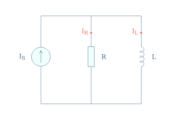
A complementary circuit to the R//C association can be made thanks to a resistor and inductor placed in parallel that we refer to as R//L association.
fig 7: R//L circuit association
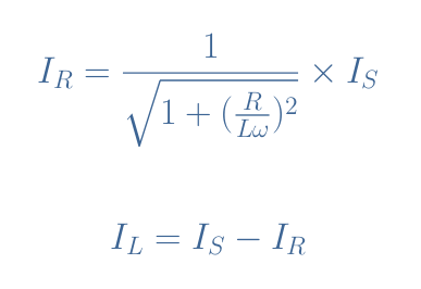
The currents are again dependent on the frequency of the AC source and their expressions are given by Equation 6:
eq 6: Current expressions in an R//L association
We choose R=1 kΩ, L=5 mF, and IS=1 A in order to show a plot example of these currents:
fig 8: Currents plots IR(ω) and IC(ω) in an R//L association
The impedance of the inductor increases with the frequency, as a result, the current IL decreases. When the frequency increases, more current goes across the resistor. Note that IR+IL is a constant equal to IS=1 A.
In practice, R//L current dividers are used as high-pass filters since high frequencies can be collected in the resistor branch. This circuit is the dual of the R//C circuit previously presented.
Conclusion
Current dividers are parallel associations of at least two electronic components that split a current provided by a source into several smaller currents.
Such configurations can provide a good value of current to match the dynamic of any stage in a circuit.
In the first section, we detail the most common and simple current divider that consists of two resistors in parallel. We demonstrate the resistive current divider relations and explain how the circuit works. Moreover, another formalism with the admittances is presented along with a simple example of an application.
Configurations with more than two resistors are presented in the second section, this kind of configuration is useful to split the power into more components and avoid accidents.
Finally, simple current dividers with reactive components are shown in the last section. Due to their frequency-dependent impedances, capacitors, and inductors can be used in parallel with resistors in order to divide the current on some specific range of frequencies.
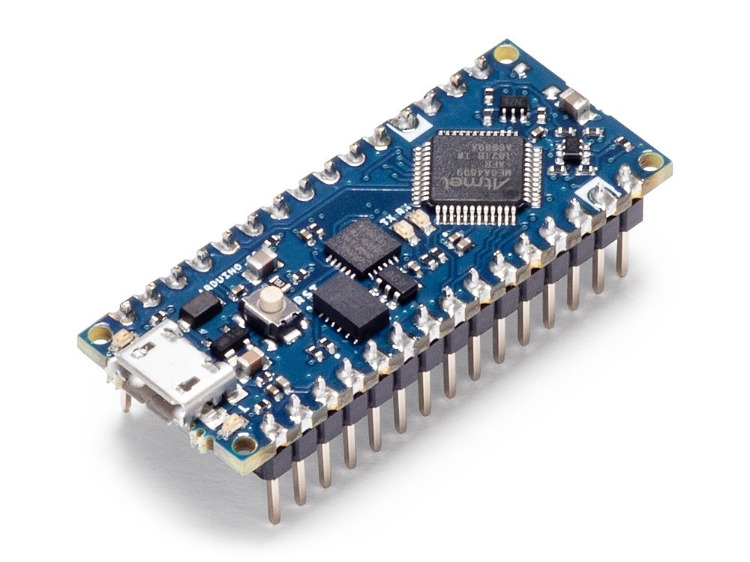
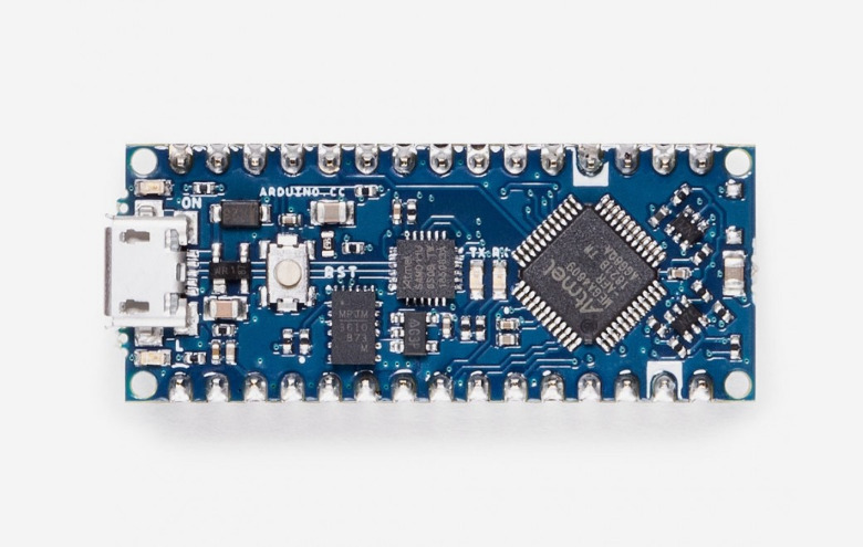
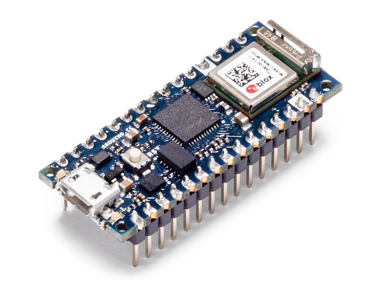
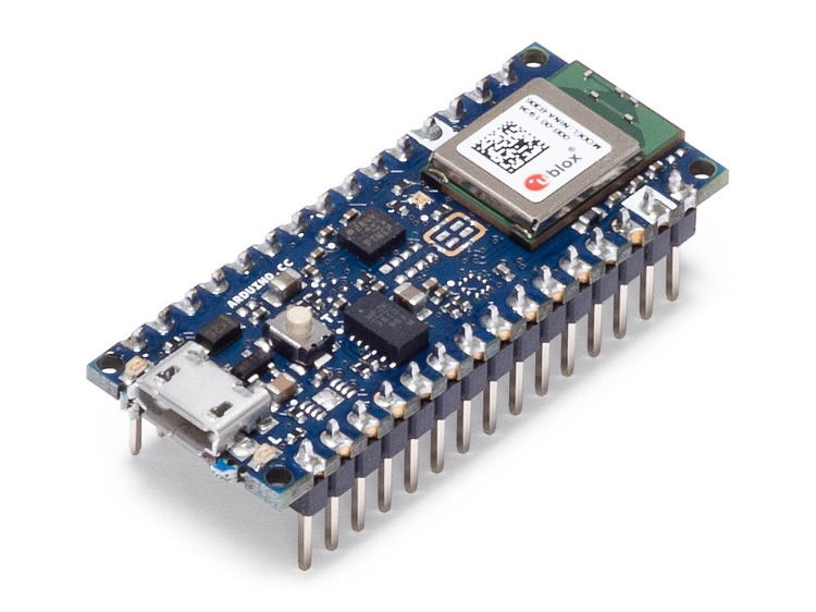
Arduino has announced a new set of boards to the Ardunino Nano family. The boards were on display last weekend at Maker Faire Bay Area in San Mateo at the Arduino booth. Banzi also delivered a talk on “The State of Arduino” at the Faire’s Center Stage. The new family of Arduino Nano boards includes: the Arduino Nano Every, the Arduino Nano 33 IoT, the Arduino Nano 33 BLE, and the Arduino Nano 33 BLE Sense.
Arduino Nano Every
The Arduino Nano Every features a ATmega4809, which is much more powerful Microchip than the ATmega328P found in the original Arduino Nano. The Ardunino Nano Every enables a Microchip ATSAMD11 Arm Cortex-M0+ processor for USB to serial communications. The Nano Every is Arduino’s 5V compatible board in the smallest available form factor: 45x18mm! The small footprint and low price, makes the Nano Every suitable for wearable inventions, low-cost robotics, electronic musical instruments, and general use to control smaller parts of a larger projects. The board comes in two options: with or without headers, allowing you to embed the Nano Every inside any kind of inventions, including wearables. The board comes with tessellated connectors and no components on the B-side. These features allow you to solder the board directly onto your own design, minimizing the height of your whole prototype.
Specification include:
Operating Voltage ; 5V
VIN min-MAX7; 21V
DC Current per I/O Pin ; 20 mA
DC Current for 3.3V Pin ; 50 mA
Clock Speed ; 20MHz
CPU Flash Memory ; 48KB (ATMega4809)
SRAM ; 6KB (ATMega4809)
EEPROM ; 256byte (ATMega4809)
PWM Pins ; 5 (D3, D5, D6, D9, D10)
UART ; 1
SPI ; 1
I2C ; 1
Analog Input Pins ; 8 (ADC 10 bit)
Analog Output Pins ; Only through PWM (no DAC)
External Interrupts ; all digital pins
LED_BUILTIN ; 13
USB ; Uses the ATSAMD11D14A (datasheet)
Length ; 45 mm
Width ; 18 mm
Weight ; 5 gr (with headers)
Arduino Nano 33 IoT
The Arduino Nano 33 IoT is based on a low power Arm® Cortex®-M0 32-bit SAMD21. The WiFi and Bluetooth® connectivity is performed with a module from u-blox, the NINA-W10, a low power chipset operating in the 2.4GHz range. Secure communication is ensured through the Microchip® ECC608 crypto chip. Available also is a 6 axis IMU, which makes them board perfect for simple vibration alarm systems, pedometers, relative positioning of robots, etc.
Specifications include:
Microcontroller ; SAMD21 Cortex®-M0+ 32bit low power ARM MCU
External Interrupts ; All digital pins (all analog pins can also be used as interrupt pins, but will have duplicated interrupt numbers)
LED_BUILTIN ; 13
USB ; Native in the SAMD21 Processor
IMU ; LSM6DS3
Length ; 45 mm
Width ; 18 mm
Weight ; 5 gr (with headers)
Arduino Nano 33 BLE
The Arduino Nano 33 BLE is a completely new board on a well-known form factor. It is equipped with an embedded 9 axis inertial sensor that makes the board ideal for wearable devices, but also for a large range of scientific experiments in the need of short-distance wireless communication. The Arduino Nano 33 BLE is different from the Nano Every and Nano 33 IoT. It is not based around a Microchip processor, rather it is equipped with a u-blox NINA B306 module, which is built on top of a Nordic nRF52840, an Arm Cortex-M4F. The Nano 33 BLE even has a 9-axis IMU on board. The board features a 32-bit ARM® Cortex™-M4 CPU running at 64 MHz. This will enable you to make larger programs than with the Arduino Uno (it has 1MB of program memory, 32 times bigger), and with a lot more variables (the RAM is 128 times bigger). The main processor includes other amazing features like Bluetooth® pairing via NFC and ultra low power consumption modes.
Specifications include:
Microcontroller ; nRF52840
Operating Voltage ; 3.3V
Input Voltage (limit) ; 21V
DC Current per I/O Pin ; 15 mA
Clock Speed ; 64MHz
CPU Flash Memory ; 1MB (nRF52840)
SRAM ; 256KB (nRF52840)
EEPROM ; none
Digital Input / Output Pins ; 14
PWM Pins ; all digital pins
UART ; 1
SPI ; 1
I2C ; 1
Analog Input Pins ; 8 (ADC 12 bit 200 ksamples)
Analog Output Pins ; Only through PWM (no DAC)
External Interrupts ; all digital pins
LED_BUILTIN ; 13
USB ; Native in the nRF52840 Processor
Length ; 45 mm
Width ; 18 mm
Weight ; 5 gr (with headers)
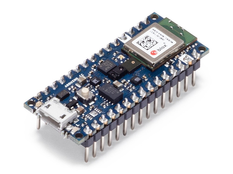
Arduino Nano 33 BLE Sense
The new Arduino Nano 33 BLE Sense is also built around the u-blox NINA B306 module, but is equipped with a much larger set of sensors in addition to the 9-axis IMU sensors for barometric pressure, humidity and temperature, light, gesture and proximity sensor, and embedded microphone. The board features a lot more powerful processor, the nRF52840 from Nordic Semiconductors, a 32-bit ARM® Cortex™-M4 CPU running at 64 MHz. This will enable you to make larger programs than with the Arduino Uno (it has 1MB of program memory, 32 times bigger), and with a lot more variables (the RAM is 128 times bigger). The main processor includes other amazing features like Bluetooth® pairing via NFC and ultra low power consumption modes. Application of the board includes environmental sensing, or human interface applications. “The main feature of this board, besides the impressive selection of sensors, is the possibility of running Edge Computing applications (AI) on it using TinyML. You can create your machine learning models using TensorFlow™ Lite and upload them to your board using the Arduino IDE.”
Specifications include:
Microcontroller ; nRF52840
Operating Voltage ; 3.3V
Input Voltage (limit) ; 21V
DC Current per I/O Pin ; 15 mA
Clock Speed ; 64MHz
CPU Flash Memory ; 1MB (nRF52840)
SRAM ; 256KB (nRF52840)
EEPROM ; none
Digital Input / Output Pins ; 14
PWM Pins ; all digital pins
UART ; 1
SPI ; 1
I2C ; 1
Analog Input Pins ; 8 (ADC 12 bit 200 ksamples)
Analog Output Pins ; Only through PWM (no DAC)
External Interrupts ; all digital pins
LED_BUILTIN ; 13
USB ; Native in the nRF52840 Processor
IMU ; LSM9DS1
Microphone ; MP34DT05
Gesture, light, proximity ; APDS9960
Barometric pressure ; LPS22HB
Temperature, humidity ; HTS221
Length ; 45 mm
Width ; 18 mm
Weight ; 5 gr (with headers)
About the new boards, Massimo Banzi, co-founder of Arduino says:
“The new Nanos are for those millions of makers who love using the Arduino IDE for its simplicity and open source aspect, but just want a great value, small and powerful board they can trust for their compact projects. With prices from as low as $9.90 for the Nano Every, this family fills that gap in the Arduino range, providing makers with the Arduino quality they deserve for those everyday projects.”
The four new boards are available for pre-order on the Arduino Store. The shipping of the boards is expected soon. The boards will come with and without headers, depending on your order. Without headers the Arduino Nano Every price at $9.90, the Nano 33 IoT prices at $18.00, the Nano 33 BLE prices at $19.00, and the Nano 33 BLE Sense prices at $29.50. The. boards with headers will cost an additional $2.
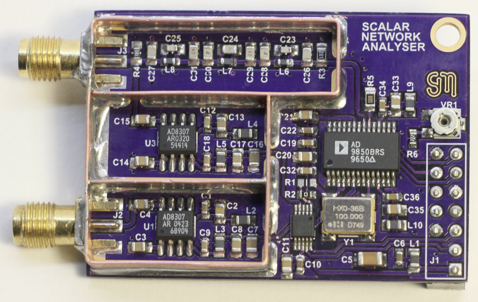
Radio Frequency Network Analyzers is one important tool required for testing the frequency response of filters and networks, but as we all know, buying a regular RF test equipment can be quite the expenditure. This was why hobbyist Stephen Merrifield, who after seeing the increased need for more RF testing capabilities as a result of increased awareness of wireless applications, decided to build his own simple scalar network analyzer with just a few components.
As the name implies, a scalar network analyzer is a type of an RF network analyzer that measures only the amplitude properties of a device over a range of frequencies. It does so by outputting a sine wave sweeping over a particular bandwidth and then measuring the amplitude of every increased frequency. So when any device is connected to the scalar network analyzer, the device’s frequency response over that bandwidth is reflected by the amplitude of the sine wave at each frequency after passing through the device.
Merrifield was able to achieve this with his design using just a combination of an AD9850 DDS chip, a multi-channel ADC, AD8307 logarithmic amplifier chip, Raspberry Pi, and general I/O interface. The DDS chip outputs the sweeping sine wave and sends it to the AD8307 log amplifier that conditions the input signal into the SNA before passing it on to the ADC for digitizing. The output of the DDS is again conditioned by another AD8307 after which it is sent as output to a second channel of the ADC to compensate for variations on the DDS’s output that could arise as a result of loads of devices being tested. The digital output from the ADC is sent via an I2C to a GPIO header.
Speaking about the flexibility of the design, Stephen mentioned that the:
“pinout matches a Raspberry Pi, but any micro-controller may be used to program the DDS and read the ADC. The analog bandwidth has been deliberately set at 30MHz. There is approximately 0.02dB variance between 1kHz and 30MHz. The noise floor averages around -69dB with shielding fitted.”
The project is entirely open-source and the firmware for the Raspberry Pi was written in C to allow for easy porting across different platforms.
Stephens Hackaday Project Log can be found here. It contains the schematic and every other resource you might need to build your own version of the scalar network analyzer.
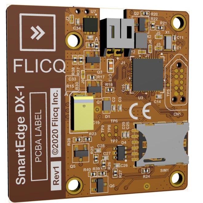
Industrial automation company Flicq has introduced its 2nd generation Edge AI smart sensor board, for Industrial Internet of Things (IIoT) with the launch of SmartEdge.
Claiming to be the world’s smallest Edge AI smart sensor board, SmartEdge delivers plug-and-play asset monitoring capability that companies can deploy anywhere. Industries are moving increasingly toward remote monitoring of equipment and they care about the flexibility of deploying systems where they want to as much as they do want visibility about the condition of their assets, with low latency and actionable insights.
With performance typically only available from cloud-based systems, the 2nd Gen Flicq SmartEdge delivers three-year battery-life, deep analytics and wireless connectivity. Industries continue to depend on real time insights to improve their operating efficiency and Flicq is pushing the edge computing performance envelope to achieve lower latency and deliver the best analytics capabilities in an extremely small form-factor.