New Enterprise Network Security Solution based on Intel Xeon Processor D-2100
IBASE Technology Inc. , a leader in the manufacture of network appliances and embedded systems, is pleased to announce its latest FWA8600 1U rackmount network computing appliance based on the Intel Xeon D-2100 processor product family and with up to 25 GbE ports. This highly scalable system is designed for managing data driven workloads and enabling robust levels of performance in enterprise network security, Unified Threat Management and WAN optimization applications.
The FWA8600 supports up to 128GB RDIMM with four DDR4-2666 DIMM sockets and one Intel I210-AT Ethernet controller. The device comes with network interface card (NIC) slots to accommodate up to three IBN cards with 8x GbE ports each and one IBN-P401Q card for a maximum of 25 GbE ports. For flexible I/O connectivity and expansion features, it offers a PCIe x8 slot, an M.2 expansion slot to interface with SATA 3.0 and PCIe x4 bus for high data throughput, as well as two USB 3.0, and an RJ45 serial console with LCM display for easy operation. LAN bypass is available in certain configuration.
“The FWA8600 features Intelligent Platform Management Interface (IPMI) 2.0 with the IBASE IDN100 module to allow users to remotely manage and monitor systems even without an operating system,” said Jason Ko, senior product manager at IBASE. “As an ideal platform for cloud computing and data centers, it also supports Trusted Platform Module (TPM 2.0) to provide hardware-based security data that encrypts data and protects authentication credentials from hackers.”
Furthermore, IBASE has verified the solution as an Intel Select Solution for uCPE that integrates the Ubuntu operating system and Intel Xeon D processor. These verified designs will benefit CSPs, telecom equipment manufacturers (TEMs), internet service vendors (ISVs), and enterprises in implementing uCPE and SD-WANs technologies with enhanced network performance and flexibility.
Reduced time to market and total cost of ownership with optimum flexibility, industrial-grade ruggedness, easy maintenance and long life support
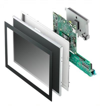
ADLINK Technology, a global provider of leading edge computing solutions that inspire creative user experiences across industries, is pleased to introduce its new generation SP-KL Smart Panel series. Based on the success of the previous generation SP-AL panels that were adopted across a wide range of fields, the versatile all-in-one open frame SP-KL panel computer offers strong performance and flexible configuration with a high level of modularization. Coupled with ADLINK’s unique Function Module (FM) design, the SP-KL speeds up prototyping based on application requirements with reduced time, effort and cost. System integrators, integrated solution providers, and brand vendors can all achieve project success in transportation, retail, hospitality, industrial automation, healthcare, gaming and other applications.
To accelerate TTM, lower TCO, and enhance design flexibility, ADLINK’s Smart Panel exceeds common application demands with a modular design, enabling custom selection of touch panel type, display size, mainboard, I/O interface, and heat sink. To empower application-specific features, function enhancement and I/O expansion are fully supported through ADLINK’s FM board or I/O boards from partners and clients. “ADLINK’s Smart Panel provides a flexible embedded building block solution, enabling users to fast-track development, verification, and validation of smart devices while enjoying significant savings in time, money and resources. These are all key success factors for our customers,” explained Fabio Zhuang, Product Manager of ADLINK’s Embedded Platform and Modules Business Unit.
The newly released SP-KL fulfills the modular design requirements of our customers, offering a choice of 7-inch to 21.5-inch 16:9 displays, P-CAP or resistive touch panels, mainboards powered by Intel Core™ i3-7100U/i5-7300U/i7-7600U processors, support for Windows 10 and Linux operating systems, and wide-ranging built-in I/O interfaces. To accommodate I/O expansion needs, FM boards can be customized to cater to vertical applications and connect to an external power supply to support power-hungry peripherals such as graphics cards.
To maintain long-term reliable operation, all Smart Panel series feature robust construction, meeting or exceeding rigorous industry standards. The mainboard supports a wide operating range from -40˚C to +85˚C, rugged SODIMM, wide DC input voltage range, overvoltage protection (OVP) and undervoltage protection (UVP). For environments in which excessive moisture and contaminants are possible, all Smart Panel series provide IP65-rated resistance without the use of adhesives. In addition, the SP-KL’s modularity and advanced mechanical design allow for easy and fast maintenance. The SP-KL further provides long life support, with the proven stability of Intel® Core™ i3/i5/i7 U-series processors and industrial-grade display modules, alleviating concerns for long-term supply availability.
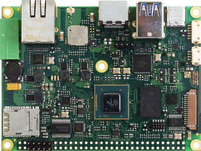
The Multimedia CPU i.MX 8M from NXP (4x ARM® Cortex®-A53 (64 Bit) with 1.5GHz & Cortex®-M4 CPU) is perfect for applications with demanding graphics in building automation, all kinds of HMI in industry and medical technology, as well as POS and POI terminals. With Linux on the Cortex®-A53 cores and FreeRTOS on the Cortex®-M4 core, NXP continues its heterogeneous concept and offers an ideal possibility for real-time processing.
For graphics processing the CPU offers OpenGL/ES 3.1, OpenGL 3.0, Vulkan, OpenCL 1.2 as well as the playback of videos up to 4Kp60. F&S Elektronik Systeme (manufacturer of embedded boards for more than 20 years with headquarters in Stuttgart) has placed this powerful CPU on the new Single Board Computer armStone™MX8M (PicoITX format). Up to 8GB LPDDR4 RAM, 1GB SLC NAND Flash and additionally up to 64GB eMMC, as well as USB3.0, Audio IN/OUT/MIC, Gigabit Ethernet, mPCIe (SIM Slot), MIPI CSI, 3x I2C, SPI, 4x UART, CAN and SDIO (uSD Slot) are available. 2x LVDS (up to FullHD) and DVI up to 4k are available for display interface. A resistive or PCAP touch panel is connected via I2C. Another option is an OnBoard WLAN/BT module (pre-certified) with antenna socket.
As with all armStone™ single board computers, many of the signals are on common connectors or on the 66-pin feature bus. The armStone™MX8M is powered by 5V (a pluggable 12/24V adapter is offered as an accessory), the power consumption is only a few watts. With a temperature range of up to -20°C – +70°C, the armStone™MX8M can also be used outdoors. Linux (Buildroot, Yocto follows) is available as operating system. This has already been ported by the experienced software team of F&S Elektronik Systeme. Bootloader, device tree, customized interface drivers and all tools necessary for development are available. Various security functions are made available by the Linux adaptation of F&S Elektronik Systeme.
With the F&S project guarantee F&S Elektronik Systeme accompanies the customer from the project start to the successful completion of the project. Starterkit and workshop, documents for hardware and software development and free support by the experienced engineers of F&S Elektronik Systeme GmbH are available.
The armStone™MX8M will remain available until at least 2028.
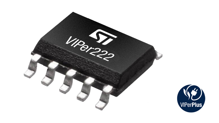
The VIPER222 device is a high performance high voltage converter that combines a 730 V rugged power MOSFET with a PWM control. The device embeds the high voltage startup and the current sense circuit, avoiding the use of extra components in the BoM. Frequency jittering spreads the EMI and allows the use of a small filter. The burst mode technique allows to obtain a very low input power consumption at light load.
High-accuracy motor commutation sensing, magnet free, total stray field immune for efficient and lightweight motor integration
The new magnet-free IPS2200 inductive position sensor is featuring high accuracy and speed, total stray field immunity, and efficient motor integration in a thin and lightweight form factor. The IPS2200 is ideal for use as an absolute position sensor in a wide range of industrial, medical, and robot applications. The sensor allows customers to cost-effectively tailor sensor design for their applications and maximize the performance of the sensor’s accuracy.
Key features
Industrial qualified, with stable operation in harsh environments and -40° to +125° C ambient temperatures
Compared to tradition resolvers the IPS2200 is up to 10x thinner and up to 100x lighter.
Off-the-shelf tools that can be used to create tailored and customized sensing elements. The custom tools can achieve coil optimization sets within 30 minutes.
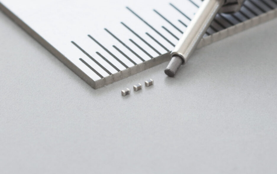
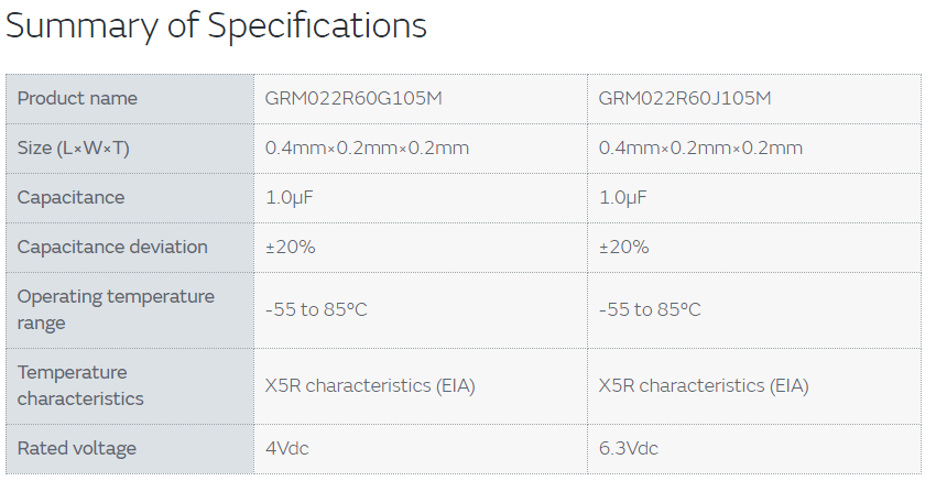
Murata Manufacturing has developed the world’s firstmultilayer ceramic capacitor with a capacitance value of 1.0μF in the 01005-inch size (0.4×0.2mm), which is increasingly used in a wide range of mobile electronic devices including smartphones. Mass production of the GRM022R60G105M with a rated voltage of 4Vdc has already started and mass production of GRM022R60J105M with a rated voltage of 6.3Vdc is scheduled to begin in 2021.
The spread of 5G smartphones and the increasing functionality and miniaturization of wearable devices is stoking the demand for further miniaturization and higher density of electronic circuitry. Among the applications, multilayer ceramic capacitors are essential components of many kinds of electronic devices and are widely used in such devices as smartphones and wearable devices. Given that approximately 900 to 1,100 multilayer ceramic capacitors are installed in a single high-end smartphone, a considerable need exists for capacitors combining smaller size with larger capacity. In particular, since multilayer ceramic capacitors with a capacitance of 1.0 μF are widely used in various devices, expanding the adoption of these new products will contribute to the further miniaturization of electronic devices.
These products have achieved approximately a 35% reduction in footprint and a 50% reduction in volume ratio compared to our existing product with the same capacitance value (015008-inch size). In addition, their capacity has increased by about 2.1 times compared to our conventional product of the same size (01005-inch size).
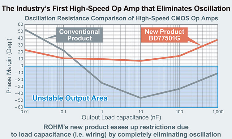
New high-speed CMOS op amp ideal for anomaly detection added to high noise immunity EMARMOUR™ series
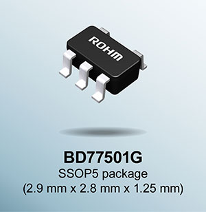
ROHM recently announced a high-speed ground sense CMOS op amp, BD77501G, optimized for industrial and consumer equipment requiring high-speed sensing, such as anomaly detection systems used in measurement and control equipment along with sensors that work with very small signals.
The proliferation of IoT in recent years has led to a significant increase in the number of electronic components used for advanced control in a variety of automotive and industrial applications. Among these, op amps are used and are capable of quickly amplifying minute sensor signals in anomaly detection systems that provide safety. However, board design can become problematic as conventional high-speed op amps are susceptible to oscillation due to capacitive loads (i.e. from wiring). At the same time, degradation of the noise environment resulting from increased electrification and mounting density is making it extremely difficult to implement noise design for small-signal devices.
In response, ROHM developed the EMARMOUR™ series of op amps and comparators*1 that have been well-received in the automotive and industrial markets due to its superior noise immunity that allows users to reduce design resources to address noise issues. This time, ROHM has expanded the lineup by adding a new high-speed type ideal for anomaly detection that prevents oscillation over the entire load capacitance range.
The BD77501G is the industry’s first op amp that not only supports high-speed amplification (high slew rate: 10V/us) required in anomaly detection and other systems, but also completely eliminates oscillation caused by load capacitance (i.e. wiring). Unlike conventional high-speed op amps that can become unstable due to load-capacitance-induced oscillation, ROHM’s new product ensures stable operation with no unwanted oscillation. In addition, whereas the output voltage for conventional products can fluctuate by ±200mV or more across the entire noise frequency band, the BD77501G provides unprecedented EMI Immunity*2 (noise immunity) that limits variation to less than ±20mV (1/10th). This enables high-speed signal amplification without being affected by load capacitance or external noise when installed in the latter stages of sensor applications, improving reliability and reducing design time.
ROHM is committed to expand the lineup of this product to automotive market in the near future.
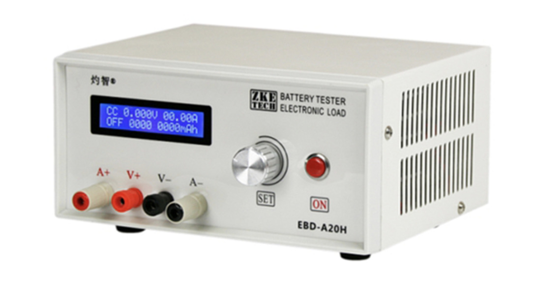
Battery testers provide an easy way for hardware designers and hobbyists to determine the genuine capacity of βatteries. There are different makes and models being sold across diverse online stores but one which stands out among all that I have used in recent times is the ZKETECHEBD-A20H.
ZKE, over the years, has produced some interesting battery testers like the handy EBD-MO5, but the EBD-A20H is probably the most versatile and professional looking one I’ve seen.
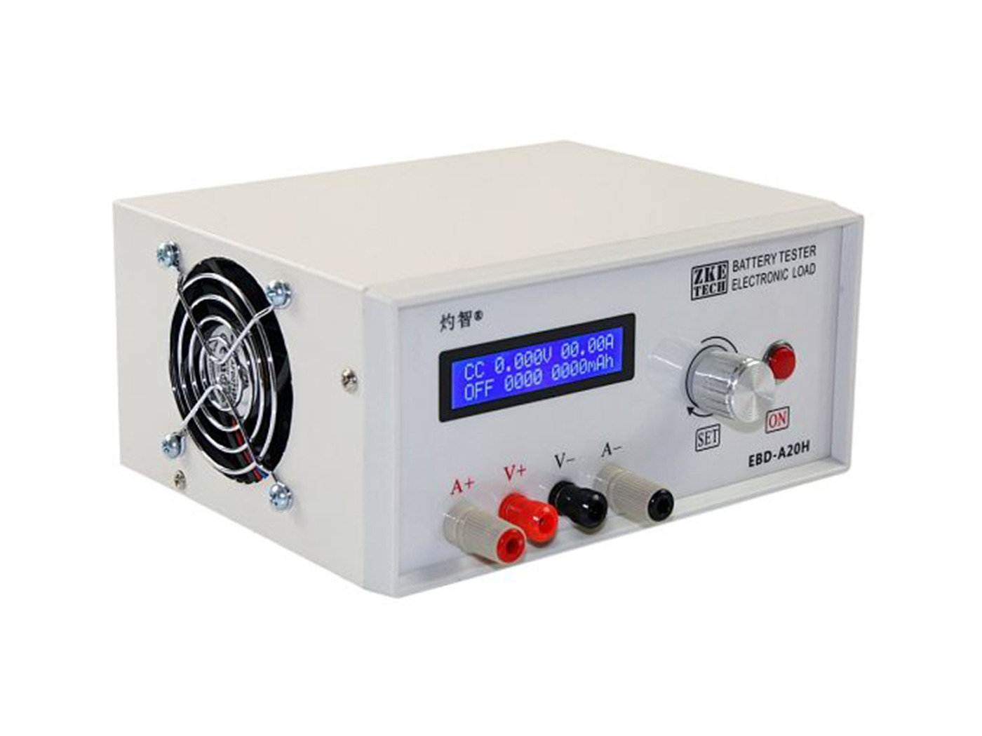
Spotting the kind of professional look that will fit right on the workbench in any lab (Professional or DIY home lab), the ZKETECH EBD-A20H is essentially a DC electronic load with multiple, controlled, battery discharge modes, that can be used to conduct various battery capacity and other power-related tests.
Some specifications of the EBD-A20H include:
Power Supply: DC 12V/1A
Voltage Setting: 0.00-30.00V, minimum step is 0.01V
Current Setting: 0.1-20.00A, minimum step is 0.01A (Current automatically limits when power is overrun)
Test mode: DSC-CC: constant discharge current for testing battery capacity or supply current/ DSC-CP: Constant discharge power for simulating constant power equipment or testing power supply
Voltage Test: 0.000-4.500V (low pressure) accuracy to 0.003V, error ±0.5% / 4.50V-30.00V (high pressure) accuracy to 0.01V, error ± 0.5%
Current Test: 0.10-20.00A, accuracy to 0.01A, error ± 0.5%
Capacity Test: Within 10Ah, resolution is 0.001Ah/ 10Ah-100Ah resolution is 0.01Ah/ Above 100Ah resolution is 0.1Ah
Discharge Power: Max 200W (It should be controlled within 90% for a long time working)
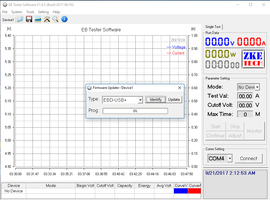
To make the visualization and analysis of test data easier, asides the LED display where the test data including voltage, current, capacity, time, power, energy, are displayed, the device also works with the “EB software” which precisely displays and can be used to plot curves, perform calibration benchmark tests, automatic current testing and also push firmware upgrades to the Battery tester device.
EB Tester Software UI
Summarized features of the device include:
Performs battery capacity, discharging and power performance tests
Supports up to 30V/20A/200W
Digital display of test data (voltage, current, capacity, time, power, energy)
Four-wire connection method
Built-in Fan for better heat dissipation
Measurement representation through PC software
The battery tester is currently available for sale on Seeed Studio at $79 without shipping fees. More information on its features and capacities is available on the product’s page on Seeed Studio’s website.
Chinese vendor Sipeed has announced a $72, open spec “Sipeed Tang Hex” SBC which supports Linux on a Xilinx Zynq-7020. This is coming after they recently launched a Sipeed MaxiCube dev based on a Kenryte K210 RISC-V chip, and a FPGA board called Sipeed Tang based on an a Gowin GW1N-1-LV FPGA selling for $5. The board goes by other names like the Lychee Sugar and the Litchi candy. The Sipeed Tang HEX can be purchased for $72 with shipping on Aliexpress, and it is referred to as the “Lychee HEX ZYNQ-7020 FPGA Development Board Raspberry pie Edition ZEDBOARD” on AliEXpress. You can also get it for 439 RMB ($62) on Taobao for people based in China, and on Amazon for $124.13 with free shipping.
The $72 price tag is fair considering the price of other open-spec Zynq-7000 SBCs such as MYIR Z-turn Board, which sells for $119, which features a Zynq-7020, 1GB RAM, and 512MB NAND flash, and the Z-turn Lite with less features, which sells for $75 and features a Zynq-7010 with a lower-end FPGA and 512MB RAM. However, the Xilinx Zynq-7020 (XC7Z020-1CLG484) features dual-core Arm Cortex-A9 processor and FPGA with 85K logic cells, 4.9Mb Block RAM, 220 DSP slices. The TANG Hex enables 1GB LPDDR3, 256MB NAND, and a microSD slot. It offers a 10/100Mbps Ethernet port, which is in contrast to the GbE on the Z-turn, and 4x USB 2.0 ports. For onboard interfaces, it features a UART, JTAG, and the 26-pin GPIO, which is unknown if it will support early Pi add-on boards. The board is powered by a 12V/3.5A DC jack, and it enables a power button and 2x user LEDs. There is no HDMI output/input just like the other boards.
The SBC specifications look ok, but it features no power supply or cables. The only information about documentation is a link to schematics. For now, there is no response from the company about the board. Hopefully, we will get better documentation about the board from the company because the documentation available looks scattered. The board might likely be an open-source board with limited tech support. The Sipeed TANG Hex is available at AliExpress for $72.47 plus $1.05 shipping to the U.S. and in China at Taobao for 439 RMB ($62) plus shipping and at Amazon for $124.13 with free shipping which is handled by it’s a company or reseller called Taidacent. Sipeed’s website does not contain enough information about the board, however, you could find more information on Sipeed’s wiki.
Sometimes, a precise value of voltage is needed as a reference or simply before a specific stage of a circuit that requires less power. Voltage dividers are a simple resolution to this problem as they take advantage of the fact that a voltage can be dropped across components put in a series configuration.
The most common type of voltage divider is based on the series association of two resistors, we present in detail this type of configuration in the first section of this tutorial.
By keeping the same architecture, resistors can be replaced by reactive components such as capacitors or inductors. These different types of voltage dividers are presented in two other sections.
Presentation
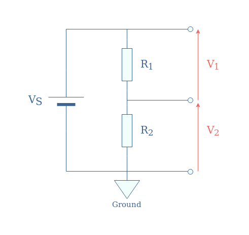
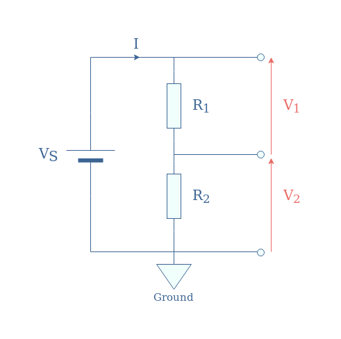
fig 1: Illustration of a resistive voltage divider
In Figure 1, we present the most common and simple configuration for a resistive voltage divider:
In the following, we will label this configuration “R1-R2“.
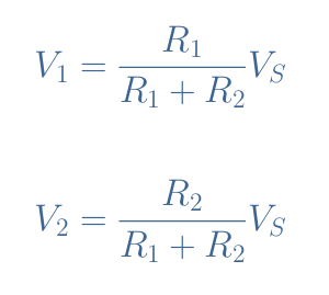
We can first of all note that according to Kirchoff’s Voltage Law, V1+V2=VS. This relation can be rewritten thanks to Ohm’s law into VS=(R1+R2)×I.
Since V1=R1×I, V2=R2×I, and I=VS/(R1+R2), we obtain in Equation 1 the following voltage divider formulas:
eq 1: Resistive voltage divider relations
It is interesting to note that both dimensionless factors for V1 and V2 in Equation 1 can range from 0 to 1. As a consequence, both signals V1 and V2 can range from 0V up to the source value VS.
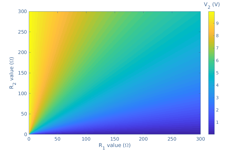
With a data program, it is possible to plot every possible value that V1 or V2 can take depending on R1 and R2 such as shown in Figure 2. For this example, we chose to plot V2 with VS=10 V and R1,R2=[0;300] Ω.
fig 2: Map of the possible values for V2
Often, voltage sources or current sources can only provide a fixed value of voltage or current. Some stages of a circuit, however, need lower values that the source is providing.
A simple voltage divider in which resistors values are appropriately chosen can provide any voltage value between 0 V and the source value, it constitutes a good solution to attenuate the source before a specific stage.
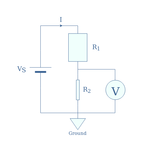
Another application in which resistive voltage dividers are suitable is the measure of high DC voltages. We illustrate this approach in Figure 3:
fig 3: Process to measure a high DC voltage
Note that the shape of the resistors is voluntarily modified to reflect the ratio R1/R2.
In order to protect the voltmeter (and its user) from measuring directly the high voltage VS, only a small fraction is measured by the voltmeter corresponding to R2/(R1+R2)×VS. The display is then corrected by multiplying the measurement by the same value that the high voltage was divided with.
For example, if R1/R2=99, the voltmeter measures only 1% of VS. The voltmeter will then display on the screen the exact value of VS by multiplying the measurement by 100.
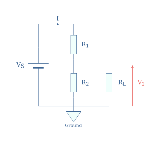
Loaded voltage divider
We consider now the same voltage divider R1-R2 as presented in Figure 1 but with the additional presence of a load RL at the terminals of R2:
fig 4: Illustration of a resistive voltage divider with the presence of an output load
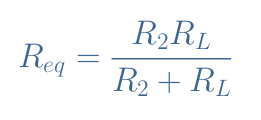
We will demonstrate the expression of V2. First of all, we express the equivalent resistance Req of the R2//RL parallel association:
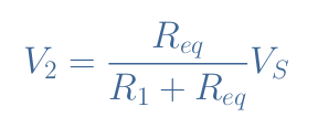
We then apply the formula of the voltage divider (Equation 1) to the voltage divider R1-Req:
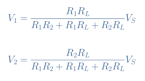
If we develop and rearrange this expression, we obtain V2 as a function of R1, R2, RL, and VS. Moreover, if the output load is instead connected to the terminals of R1, we can also write the expression of V1 similarly to obtain both formulas for the load voltage divider:
eq 2: Resistive loaded voltage divider relations
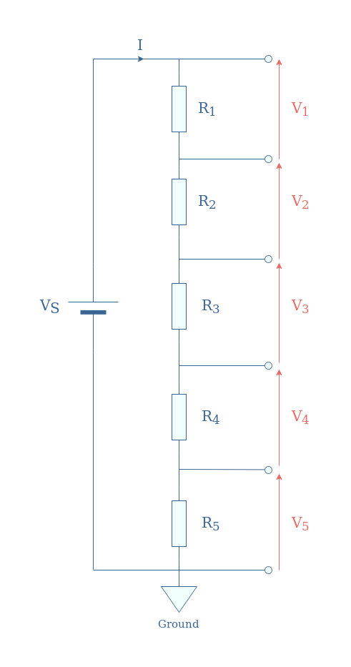
Voltage divider network
A voltage divider network is the association of three or more resistors in series that act as a voltage divider. In the following Figure 5, we illustrate a voltage divider network with five resistors:
fig 5: Illustration of a resistive voltage divider network
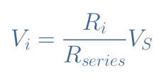
If we note Rseries=R1+R2+R3+R4+R5 the equivalent resistance for the series association of resistors, each voltage is given by Equation 3:
eq 3: Voltages expressions in a voltage divider network
For a voltage divider network with N resistors, Equation 3 remains valid with Rseries=R1+R2+…+RN.
We need to conclude the sections about resistive voltage dividers by saying that they are highly inefficient because the resistors dissipate power by Joule’s heating. For obvious safety reasons related to these power losses, they are only used for low-power applications such as for example in microelectronics to drive MOSFET and Bipolar amplifiers.
For high-power applications, reactive voltage dividers are preferred since they do not dissipate to much power by Joule’s heating.
Reactive voltage dividers
Alternative voltage dividers can be based on a capacitor or inductor instead of a resistor, they are known as reactive voltage dividers.
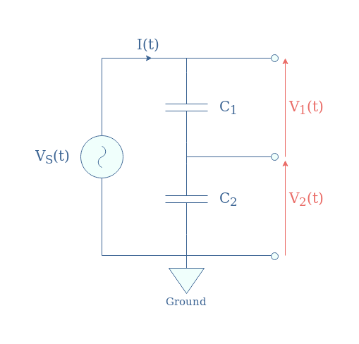
Capacitive voltage dividers
Capacitive voltage dividers are based on the same architecture as presented previously in Figure 1 by replacing the resistors with capacitors. Since the reactance of capacitors is given by 1/Cω, capacitive voltage dividers only work in the AC regime.
The advantage of using capacitors is that they present much lower power losses at high frequencies than a resistor. Indeed, we have seen in the dedicated tutorial about AC Resistance that the AC impedance tends to become much higher than the DC impedance for high frequencies due to the skin effect.
Moreover, capacitive voltage dividers are usually used for voltages above 100 kV in RMS value. The reason why is that resistive voltage dividers dissipate too much heat for high voltages, while ideal or near-ideal capacitors store the energy in the form of an electric field and release it in the circuit.
fig 6: Illustration of a capacitive voltage divider
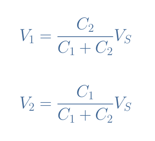
If we label V1, V2, and VS the RMS values of the voltages, it is easy to demonstrate again that they follow similar relations as presented in Equation 1. However, since the impedance here is proportional to 1/C, the subscripts of the numerator change:
eq 4: Capacitive voltage divider relations
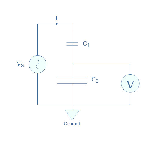
A similar circuit of Figure 3 by replacing the resistors with capacitors is suitable to measure high AC voltages. Since the voltage drop in a capacitor is proportional to 1/C, a large voltage drop will occur in the small capacitor C1:
fig 7: Process to measure a high AC voltage
Inductive voltage dividers
We do not encounter in the literature the term “inductive voltage divider” but we rather refer to this circuit as an autotransformer. An autotransformer is a single inductor with multiple tapping points, which can be seen as multiples inductors connected in series.
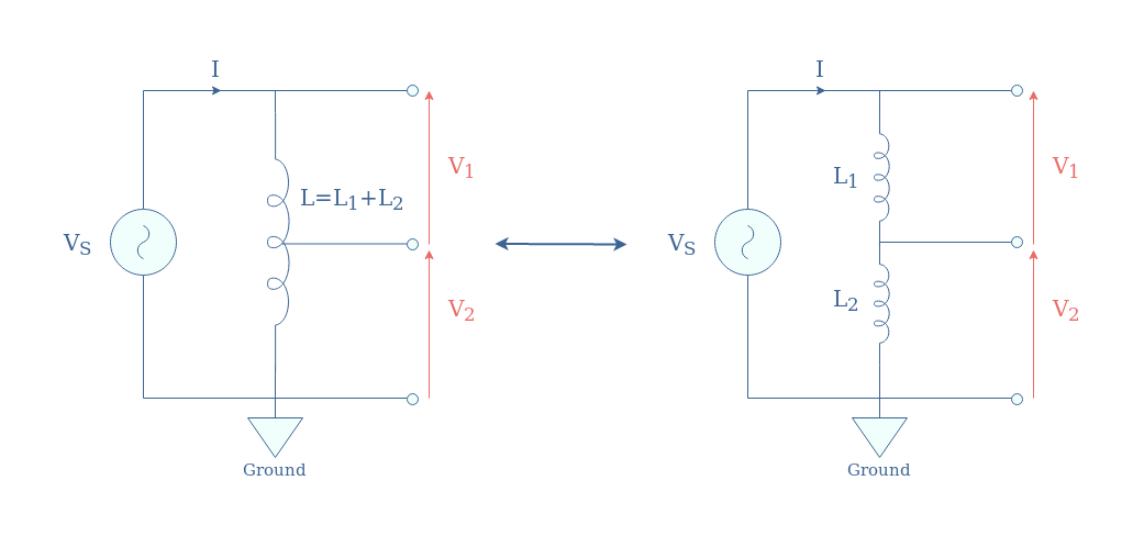
In Figure 8, we present an autotransformer with one intermediary tapping point, which corresponds to the simpler design and is equivalent to two inductances in series:
fig 8: Illustration of an autotransformer (left) and its equivalent “inductive voltage divider” (right)
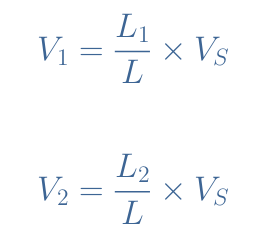
If we note N1 and N2 the number of windings in L1 and L2, the ratio of voltages is simply given by V2/V1=N2/N1.
Similarly to capacitive voltage dividers, an autotransformer is suitable for high-power applications since the inductors store the energy in the form of a magnetic field and release it to the circuit, producing no heat dissipation.
When drawn as an equivalent “inductive voltage divider”, the voltage formulas of the autotransformer are given by Equation 5:
eq 5: Autotransformer relations
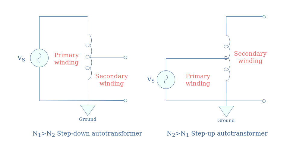
Usually, autotransformers are most found in high-power transmission lines to step-down or up voltages. Step-down and step-up autotransformers are easy to recognize by the proportion of their primary and secondary winding:
fig 9: Step-down and step-up autotransformers
Conclusion
Any voltage divider consists of at least two components in a series configuration in which a voltage drop can happen. The output is taken between a tapping point and the reference of the circuit (ground).
The goal of such circuits is to obtain a smaller voltage output value than the source supply VS in order to respect the dynamics of the incoming stage of the circuit. The output corresponds to a fraction of the source, between 0 and VS.
For low-power applications, we rely on resistive voltage dividers based on resistor components. We detail the demonstration of the output voltage formulas, the modification that an output load provides, and the existence of voltage network dividers, where many resistors can be interconnected in series in order to simultaneously provide different voltage outputs.
The disadvantage of resistive voltage dividers is that they are not suitable for high-power applications such as grid distribution. For this function, reactive voltage dividers are preferred as they do not dissipate large amounts of heat such as resistors.
Reactive voltage dividers are divided into two categories: capacitive and inductive, depending on which basic component is used. For capacitive voltage dividers, capacitors are connected in series and the largest voltage drop occurs in the smallest capacitor as their reactance is inversely proportional to their capacitance.
Inductive voltage dividers are most referred to as autotransformers, the largest voltage drop occurs, similarly with resistive voltage dividers, in the largest inductor as their reactance is directly proportional to their inductance.
While capacitive voltage dividers are mostly found in multimeters to probe high voltages, inductive voltage dividers are used in the grid distribution to step-down or step-up 50 Hz high-voltages. A typical example would be that autotransformers establish links between countries that not necessarily use the same voltages in their transmission lines.