Zynq UltraScale+ MPSoC based FZ3 Card for Deep Learning

MYIR introduces a powerful FZ3 Card for deep learning. Built around the Xilinx Zynq UltraScale+ ZU3EG MPSoC, with Computing Power up to 1.2TOPS and MobileNet up to 100FPS, the FZ3 Card is an ideal machine learning hardware for developers to develop, validate or just directly integrate it into their end artificial intelligence (AI) products, thus accelerating their AI applications.

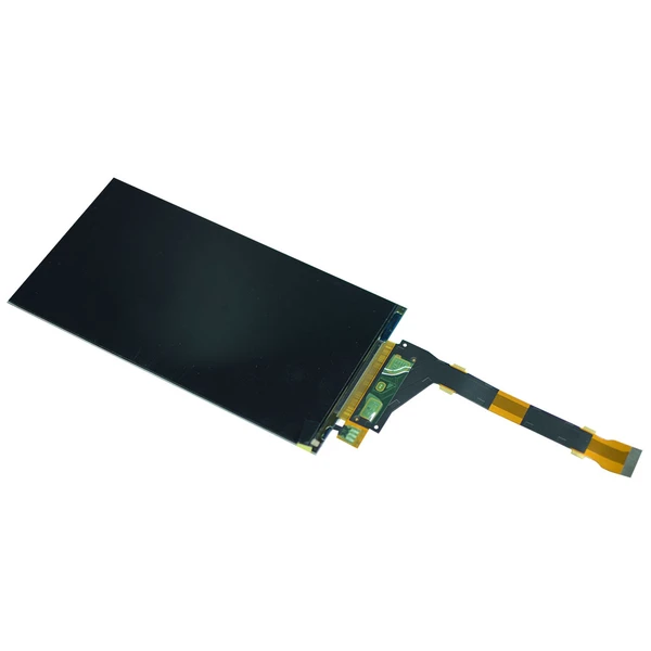
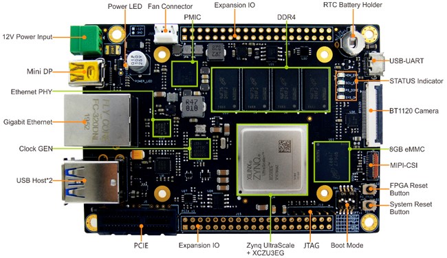
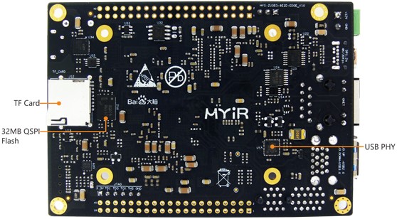
The FZ3 Card (with the installed radiator) has the size of 100mm by 70mm, integrated with 4GB DDR4, 8GB eMMC32MB QSPI Flash and 32KB EEPROM, many peripherals are routed out on board including USB 2.0, USB 3.0, Gigabit Ethernet, TF, DisplayPort (DP), PCIe interface, MIPI-CSI, BT1120 camera, USB-UART, JTAG, IO expansion interfaces.

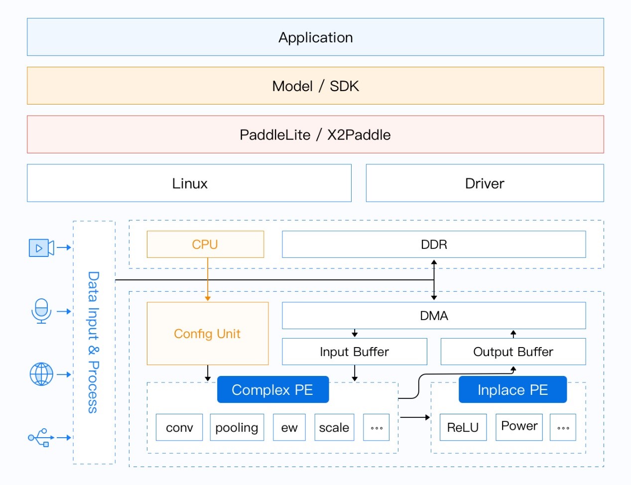
The Card is also provided with rich software resources, it’s able to run PetaLinux 2019.1, and fully compatible to use Baidu Brain’s AI development tools like EasyDL, AI Studio and EasyEdge, which makes it much easier for developers to quickly leverage Baidu-proven technology or deploy self-defined models, enabling faster deployment. Typical applications of the FZ3 Card are AI camera, AI computing device, robotics, intelligent car, intelligent electronic scale, patrol UAV and other embedded intelligent applications.

Software Architecture of FZ3 Card

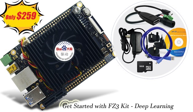
MYIR provides FZ3 Kit as a whole development kit, it contains the FZ3 Card and some necessary accessories including one 12V/2A power adaptor, one 16GB TF card, one mini USB cable and one mini DP to HDMI cable. The FZ3 Kit is priced at only $259/unit.

More information about the new products can be found at http://www.myirtech.com/list.asp?id=630

Littelfuse Adds 105ºC Rated, 800V Solid State Relay to Product Line

Littelfuse, Inc. a global manufacturer of leading technologies in circuit protection, power control, and sensing, announced the PLA172P OptoMOS® Relay, an 800 V normally-open single-pole 6-pin solid-state relay (SSR). It is the first solid-state relay in the Littelfuse product portfolio that comes with guaranteed electrical parameters at 105 °C ambient operating temperature.

“The PLA172P is an extension to our OptoMOS solid-state relay product line, offering our highest voltage rating (800V) in a surface mount SSR Flatpack package,” said Steve Andrezyk, Global Product Manager at Littelfuse. “It also has our highest temperature range in a solid-state relay, extending our operational temperature range from 85 ºC up to 105 ºC, enabling hardware engineers to precisely design their circuits at very challenging temperatures.”

This combination of high voltage rating, high-temperature range, and surface-mountable packaging is recommended for applications including:

  • Industrial
  • Instrumentation
  • Medical
  • Isolation Test Equipment
  • Battery Isolation Monitors
  • Industrial Solar Field Isolation Monitor

The PLA172P OptoMOS relay includes these key benefits:

  • Replaces electro-mechanical relays (EMRs) that are bulky and prone to failing drop tests
  • Unique device pinout provides more than 6.8 mm of pad-to-pad separation between the high voltage output pins preventing arcing
  • 5000 VRMS input-to-output isolation
  • 5 mA low input control current over operating temperature range

Application – Isolation Current Monitor

Isolation current monitor circuits for higher voltage systems >400 V require high blocking voltage, low off-state leakage current relays with high input-to-output isolation rating to prevent potential lethal current conduction to the system chassis. The PLA172P relay’s 800 V load voltage rating with 100 mA load current capability provides additional design margin compared to the more common 600 V rated SSRs, particularly on noisy AC power line applications and high voltage battery applications. The 105 °C specifications including the low 5 µA maximum off-state leakage current rating in conjunction with the low on-resistance, making it the ideal choice for high precision isolation current monitor applications.

Availability

PLA172P OptoMOS relays are available in tape and reel format in quantities of 1,000 as well as 50 per tube. Sample requests may be placed through authorized Littelfuse distributors worldwide. For a listing of Littelfuse distributors, please visit Littelfuse.com.

View Product Page

Download Datasheet

Advantech Launches Edge Network Appliance Designed Ready for 5G & Wi-Fi 6

Advantech a global leader in IoT, today announced its new FWA-1112VC network appliance which introduces a series of innovative features to its widely adopted range of entry and mid-level white boxes for software-defined WAN (SD-WAN) and universal Customer Premises Equipment (uCPE). Major upgrades include extended connectivity choice, with dual 10GbE SFP+ and PoE+ support, in addition to a future-proof design ready to adopt coming 5G and Wi-Fi 6 technologies. The FWA-1112VC is a fanless and compact platform that fits working environments where noise levels need to be kept down. It also supports wide operating temperature range to meet edge deployment needs, extending uCPE use cases from enterprise to smart city and industrial IoT.

The new Advantech FWA-1112VC white-box appliance is based on Intel Atom® processor and has been cost optimized to run SD-WAN and network security workflows. It provides flexible WAN connectivity options including 5G, 4G/LTE, Wi-Fi 5, Wi-Fi 6 and 10 GbE SFP+ configurations. Encryption and compression acceleration are supported using Intel® QuickAssist with DPDK providing the technology needed to accelerate packet handling without consuming additional resources. Additional features include PoE+, eMMC and dual 4G/LTE support and improved surge protection. Its fanless design allows for wide operating temperature ranges from -20 ⁰C up to +70 ⁰C to meet harsh environments requirements at the edge.

  • Fanless and compact with wide operating temperature range extends SD‑WAN and uCPE use cases to Smart City and Industrial IoT
  • The new cost-optimized FWA-1112VC also features 10GbE SFP+ connectivity to meet increasing WAN speed demands
  • The platform has been validated by leading uCPE and service provider partners ADVA and Combridge, member of Deutsche Telekom Group

The FWA-1112VC has been validated by leading partners including ADVA and Combridge. ADVA Ensemble Connector is a virtualization platform that enables agile, automated delivery of multi-vendor software services. Combined with the new FWA-1112VC hardened appliance, it provides an open edge platform that gives service providers access to a wide variety of uCPE use cases including recent ADVA-Advantech joint smart city blueprint. Combridge, member of the Deutsche Telekom Group, offers data and internet services to business partners. By integrating the new FWA-1112VC as part of their portfolio, they are able to target new application areas at the edge and be prepared to bring the benefits of 5G and Wi-Fi 6 technologies to their customer base.

“For over 20 years, Advantech has been providing innovative networking platforms trusted by top equipment manufacturers and service providers to transform global networks,” said Sandy Chen, Head of Network Appliances & Hyper Converged Network Servers, Cloud IoT Group, Advantech. “The FWA-1112VC is another step forward in our pioneering white-box uCPE offering that extends the cloud to the edge supporting fully disaggregated network models that allow service providers and enterprises to drive innovation in the 5G and IoT era.”

“The uCPE market is rapidly expanding to include additional application such as IoT and 5G,” commented James Buchanan, Senior Vice President and General Manager Edge Cloud at ADVA. “The new Advantech FWA-1112VC supports that evolution with its enhanced support for wireless technologies and extended temperature range. It will be a welcome addition for those looking to expand the deployment of virtualized applications.”

“We already use Advantech’s existing portfolio in our custom tailored solutions, enabling us to deliver highly customised, yet cost-efficient solutions to the market,” said Endre Magyari, Business Development Director at Combridge. “I am very confident, that this new tiny yet powerful device Advantech FWA-1112VC will further enhance our capabilities and competitiveness in the SD-WAN market, considering its advanced 5G and Wi-Fi 6 technologies and size/cost efficiency.”

The FWA-1112VC is available for evaluation and will be available for customer shipping in September 2020.

Detailed product information: https://www.advantech.com/

Calculate Size of Solar Panel, Battery Bank and Inverter (MS Excel Spreadsheet)

Design of solar panel/battery bank and inverter using this Excel Sheet.

This MS Excel spreadsheet calculates the following:

  • Total Demand Load
  • Size of Solar Panel
  • Select Type of Connection of Solar Panel
  • Select Rating of Each Solar Panel
  • Energy from Solar Panel as per Daily Sun lights
  • Size Battery Bank
  • Select Type of connection of Batteries in Battery Bank
  • Size of Inverter

Calculate Size of Solar Panel, Battery Bank and Inverter (MS Excel Spreadsheet) – [XLS]

How Miromico Designed the Industry’s Smallest LoRaWAN Module for the IoT

Miromico develops innovative IoT solutions in volume using state-of-the-art wireless technologies, including LoRaWAN, Sigfox, and NB-IoT. The Zurich, Switzerland-based company also provides design services in the areas of ICs, electronic systems, and software. By:Christine Young

The company is disrupting the design of sensors by tapping into novel wireless communications technologies. In doing so, Miromico is producing low-cost, battery-powered sensors that operate for more than 10 years. To facilitate fast prototyping and development for its customers, its designs are based on standard Miromico modules that can be used out of the box. Using these modules, designers can bring wireless connectivity to a variety of products.

While many of the company’s LoRaWAN modules are based on chipsets that are large and do not provide security, IoT applications demand the opposite. “In LoRaWAN, our clients want to have access to novel and highly integrated technologies. We needed for the extension of our LoRaWAN module family a microcontroller that is small, offers security, and is cost competitive. At the same time, we also wanted to have a strong partner with competence in security,” explained Dr. Schekeb Fateh, who works in business development at Miromico.

The company found its microcontroller solution in the MAX32625/MAX32626 microcontrollers from Maxim’s family of ultra-low-power microcontrollers, which are ideal for IoT applications and wearables. The FMLR-6x-x-MA62x, which measures just 8.6mm x 9.3mm, is the world’s smallest LoRaWAN module. It can send with up to 20dBm and receive with a sensitivity of -137dBm and offers security on the node. Designers can place the module in a high-density urban or long-range rural environment and connect to a large variety of sensors via LoRaWAN.

The MAX32625 and MAX32626 are Arm® Cortex®-M4 devices with floating-point unit, providing 512KB flash, 160KB SRAM, flexible power modes, an intelligent PMU, and dynamic clock and power gating to help optimize performance and power consumption. For designs that require always-on monitoring, the microcontrollers have internal oscillators that run at 4MHz for maximum battery life (they can also run at 96MHz for high performance). To meet security needs, the devices have a trust protection unit (TPU) that provides ECDSA and modular arithmetic acceleration support, a true random number generator, and a secure boot loader.

Miromico was able to move from idea to mass production of its LoRaWAN module in less than six months. The company also met its power, form factor, and security targets using the MAX32625 and MAX32626.

Designers who are ready to evaluate LoRaWAN technology can take advantage of the Maxim DARWIN LoRaWAN Starter Kit. The kit includes a customizable IoT button as an example for an end device, a development board with a Maxim FMLR module for fast prototyping, and a Tabs hub LoRaWAN gateway for connectivity with a backend and application server provided by the Swiss partner company, InstaSolution.

This blog post was adapted from the Miromico customer testimonial. Read the testimonial to learn more about the Miromico story. [via]

HiSilicon & Nowi Introduce Energy Autonomous NB-IoT Platform: a Power-free Solution in the Smallest Size Possible

HiSilicon and Nowi’s continued collaboration has led to a 2nd generation Energy Autonomous NB-IoT platform optimised for ease-of-use and form factor. New Internet of Things applications are now possible, where physical size is limited and ‘Plug & Forget’ indefinite operation is required.

HiSilicon (Shanghai) Ltd and Nowi Energy B.V. today showcased the 2nd generation of their Energy Autonomous NB-IoT platform. The device acts as a sensor hub that can transmit via NB-IoT while operating indefinitely through its energy harvesting capabilities. It is based on HiSilicon’s Hi2115 NB-IoT solution and Nowi’s leading NH2 energy harvesting power management IC. The solution removes the need for manual intervention (changing batteries) or cabling to supply power in applications that become zero maintenance.

Building upon the success of the 2019 collaboration (link), HiSilicon and Nowi have optimized the design to resolve customers’ challenges and satisfy new, stricter market requirements to broaden the variety of applications addressed. The platform combines connectivity and energy harvesting in the smallest size possible and offers an open slot on which various sensors can be placed depending on the application need. As such the platform can act as the backbone of countless connected sensor solutions.

HiSilicon and Nowi are offering the reference design and the corresponding schematics for others to build their solutions upon.

Charles Sturman, Senior Director Product Marketing at HiSilicon said

“Many IoT applications require super long deployment lifecycles and direct power connectivity is often not possible. As such, energy autonomy is becoming an important factor. Our collaboration with Nowi addresses these demands as their next-generation NH2 device reaches efficiency and size targets which are changing the rule-book on Energy Harvesting. At HiSilicon, we aim towards a fully connected, intelligent world and such partnerships are crucial to achieve this vision. “

The Energy Autonomous NB-IoT V2 Platform solves multiple challenges:

  • Provides a ‘Plug & Forget’ solution capable of multiple transmissions per day indefinitely
  • Offers a platform that can be tailored to fit many sensor applications with minimal effort
  • Enables applications that were previously unable to use NB-IoT with energy harvesting due to size constraints
  • Enables both indoor and outdoor applications

Simon van der Jagt, CEO Nowi said

“From industrial IoT to Smart Home applications we see a strong need for ease-of-use, reduction in device maintenance and small form factor solutions. As such, integrated energy harvesting solutions are playing a key role in the future of connectivity. Nowi’s energy harvesting power management technology uniquely offers these advantages owing to its extremely small PCB assembly footprint, top energy harvesting performance and ease of implementation. We are excited to team up with HiSilicon and help customers on their way by offering the schematics of this new reference design platform. Nowi’s NH2 PMIC is becoming available in Q4 of 2020 for high volume customers.”

The 2nd generation Energy Autonomous NB-IoT board has a significantly decreased PCB size and bill of materials. This powerful new design enables new IoT applications that require continuous operation and have fundamental constraints in form factor.

Technical Specifications:

  • 3 Transmissions per day in indoor conditions*
  • 6 Transmissions per day in outdoor conditions*
  • Can operate with a range of photovoltaic (multiple) cells
  • Dimensions: 5.5cm x 3.5cm

* Depending on the size of PV

Gravity: I2C Oxygen Sensor is on sale for $53.90

The Gravity: I2C Oxygen Sensor is based on electrochemical principles and it can measure the ambient O2 concentration accurately and conveniently. With high anti-interference ability, high stablility and high sensitivity, this arduino-compatible oxygen sensor can be widely applied to fields like portable device, air quality monitoring device, and industries, mines, warehouses and other spaces where air is not easy to circulate.

Features

  • High sensitivity
  • I2C Interface
  • Compatible with both 3.3V and 5V micro-controllers
  • Polarity protection

Specification

  • Detection of Gas: oxygen
  • Operating Voltage: 3.3 to 5.5V DC
  • Output Signal: I2C output
  • Measurement Range: 0~25%Vol
  • Maximum Measurement limit: 30%Vol
  • Resolution: 0.15%Vol
  • Sensitivity: (0.10±0.05) mA (in the air)
  • Stability: <2% (Every month)
  • Repeatability: <2%
  • Response Time: ≤15 seconds
  • Operating Temperature: -20~50℃
  • Operating humidity: 0~99%RH (no condensation)
  • Pressure Range: standard atmospheric pressure ±10%
  • Lifetime:> 2 years (in the air)
  • Dimension(L x W x H): 37 * 27 * 24.5 mm/1.46 * 1.06 * 0.97 inches
  • Weight:0.037kg

This compact dfrobot oxygen sensor supports I2C output, it can be calibrated in the air, can accurately measure the oxygen concentration in the environment. It is compatible with many mainboards like Arduino Uno, esp32, Raspberry Pi, and so on. Its effective range is 0~25%Vol, and resolution can reach to 0.15%Vol. It supports wide range input voltage: 3.3V to 5.5V. Moreover, the lifetime is as long as 2 years. With a simple Gravity interface and practical sample code, you can build your own oxygen concentration monitor easily and conveniently.

Rechargeable 100-µAh batteries come in pint-sized SMD format

TDK Corporation presents a new packing unit for CeraCharge, the world’s first SMD technology solid-state rechargeable battery, in the compact size EIA 1812 (4.4 x 3.0 x 1.1 mm3). The packing unit (B73180A0101M199) includes 10 blister-packed CeraCharge batteries that come in a vacuum-sealed plastic bag. The components are manufactured in regular series production and are suitable for test purposes, prototype construction and the installation of pilot lines. The packing unit can be obtained quickly and easily from selected TDK service distributors.

CeraCharge can be recharged more than 1,000 times, and has a capacity of 100 µAh at a nominal voltage of 1.5 V. Currents in the range of a few mA can also be rapidly drawn. Thanks to the SMD technology, it is simple to fit the batteries and process them in reflow soldering processes, which in turn, reduces the production costs of the device. CeraCharge is designed for a temperature range of -20 °C to +80 °C.

Unlike most ordinary technologies, CeraCharge is a solid-state rechargeable battery that uses a ceramic solid as electrolyte instead of liquid electrolyte, thus eliminating the risk of fire, explosion or leakage of electrolyte fluid. In a similar way to ceramic capacitors, CeraCharge is based on multilayer technology and combines a relatively high energy density in a very compact space, with process security, when manufacturing multilayer construction components.

To increase capacity and voltage, individual CeraCharge chips can be connected in series and in parallel as required, opening up a very wide spectrum of potential uses – especially in IoT applications. For example, this could include real-time clocks, Bluetooth beacons, wearables, or energy harvesting.

5.5″ 1440×2560 High Resolution with 2 channel MIPI for VR TFT LCD- MIPI

DM-TFT55-419 is a 5.5″ High-Resolution TFT display sold for $35 on displaymodule.com

Main Features

  • 5.5″ IPS Screen
  • High resolution 1440×2560 Pixels
  • TFT Interface: 2 channel 4 Lane MIPI
  • Divding two display area by two channel MIPI
  • Be suited to VR display products development

Turn Your Arduino to a UPDI Programmer

ATtiny series of microcontrollers have, in recent times, been on the receiving end of a renewed love from the community. The processing power and new features, packed into the tiny form factor which houses the new chips have been a major contributor to their adoption, however,  one other major contributor is the existence of tools that make the process of developing embedded hardware with the chips easy. One of such tools is the jtag2updi firmware developed by ElTangas.

The Jtag2updi firmware is designed to run on MCUs like the Atmega328p, or other AVR MCU (including experimental support for atmega1280/2560, and for Logic Green LGT8F328P/D AVR clones with 32 pins or more). It enables the microcontroller to interface with AVRdude using the jtagice Mk2 protocol via a serial link and provides a bridge that allows you upload codes to the new Attiny817 family of MCUs, that use the UPDI interface.

An illustration of the process facilitated  by the firmware is provided below:

avrdude -> HW Serial interface -> Programmer MCU (e.g. Mega328P) -> SW Serial on PD6 -> Target MCU (e.g. tiny817)

The jtag2updi relationship with avrdude facilitates the use of the Arduino IDE as a development platform for the ATtiny series of microcontrollers and the fact that the firmware works on microcontrollers like the atmega328p means it can be hosted on boards like the Arduino Uno/Nano, transforming them into programmers for the new chips. Using Arduino boards like the Uno/Nano requires a few modifications like disabling the auto-reset feature of the board using the techniques described here. https://playground.arduino.cc/Main/DisablingAutoResetOnSerialConnection.

The jtag2updi firmware has gone through several iterations and most of the flaws in the previous versions have been fixed and improvements made. One of the major challenges with the past versions is the firmware freezing while waiting for a target that wasn’t working (for example, because it was connected incorrectly) or the host (for example, if you entered a slow command, like reading a 128k flash memory when you didn’t intend to, and ctrl-c hoping to “save time”), requiring a reset to reconnect to it. This has been fixed in the current version using timeouts on communication with both the host and the target.

jtag2updi has officially only been tested on tinyAVR 0-series and 1-series and ATmega 328p/168p, but it has been used widely in the community and It is expected to work on classic megaAVR x8, x4, x1, and x0 parts, as well as megaAVR 0-series and AVR-DA parts.

All of the firmware sources, build process, documentation, list of compatible devices, and build guidelines can be found on the project’s Github repo.

TOP PCB Companies