TTI, Inc., a leading specialty distributor of electronic components, is now stocking Amphenol Advanced Sensor’s line of CO2 Sensors and Infrared Dust Particle Sensors.
Amphenol’s Telaire CO2 module product line boasts over 30 patents related to the design and application of low-cost infrared gas sensing. With sensors specific to certain environments, Amphenol and TTI will be sure to have a sensor with the best calibration process, size, or performance for your application.
Along with these gas and particle sensors, Amphenol offers a line of humidity and temperature sensors for environmental monitoring applications for home, office, and even indoor agriculture.
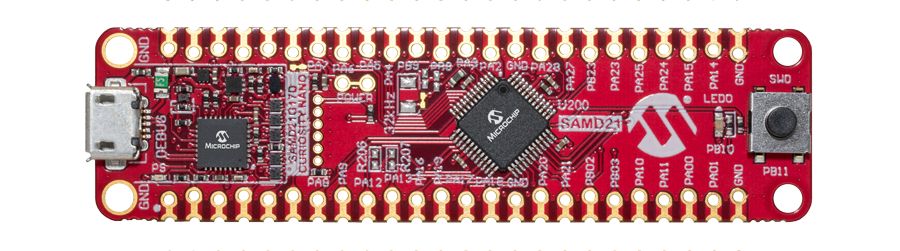
Microchip’s kit is a hardware platform designed to evaluate the SAMD21G17D microcontroller (MCU)
Microchip’s DM320119 Curiosity Nano evaluation kit is a hardware platform designed to evaluate the SAMD21G17D MCU and supported by the MPLAB® X integrated development environment (IDE). The evaluation kit provides easy access to the features of the SAMD21G17D to integrate the device into a custom design. The Curiosity Nano series evaluation kits include an onboard Nano debugger requiring no external tools to program the SAMD21G17D device. The evaluation kit is compatible with the AC164162 Curiosity Nano baseboard which allows users to quickly scale and prototype their innovative designs using the SAMD21G17D MCU.
The Curiosity Nano is an evaluation platform that provides a set of small boards with access to most of the MCU I/Os. The platform consists of a series of low pin-count MCU boards, which are integrated with the MPLAB X IDE to present relevant user guides, application notes, datasheets, and example codes. The platform features a Virtual COM port (CDC) for serial communication to a host PC and a data gateway interface (DGI) GPIO. The DM320119 Curiosity Nano evaluation kit is ideal for a variety of applications including industrial, medical, home automation, and IoT.
Features
SAMD21G17D MCU
One yellow user LED
Adjustable target voltage:
MIC5353 LDO regulator is controlled by the onboard Nano debugger
Output voltage: 1.7 V to 3.6 V
Max. output current: 500 mA (limited by ambient temperature and output voltage)
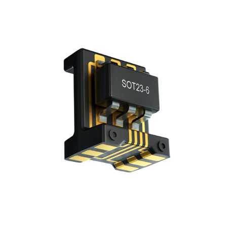
Flexible circuit boards offer numerous advantages. However, the mechanical fixation of these circuit boards is highly complex. HARTING has developed a new solution based on 3D-MID technology that is capable of replacing flexible circuit boards. Thanks to component carriers, cost savings of up to two-thirds can be achieved.
At the MID process, on the injection molded part a customized layout is applied. At the electronic assembly, the components are mounted on the desired surface.
Flexible printed circuit boards made of thin polyimide films have established themselves in many product areas thanks to their application flexibility. Populating and assembling them, however, is decidedly more complex. This is where a newly developed component carrier from HARTING enters the picture.
A standardized component carrier for electronic components
By harnessing this all new HARTING development, electronic components can be fitted directly onto the component carrier, thereby replacing flexible circuit boards. The component carrier serves as a connecting element between the printed circuit board (PCB) and electronic components such as LEDs, ICs, photodiodes and sensors.
Electronic components are mounted directly on the new component carrier in automated processes. The frequently complex processes involved in processing flexible circuit boards is dispensed with, thereby reducing costs by up to two-thirds.
The populated component carriers are delivered in tape & reel. In their standard design, the carriers can be processed in automatic assembly systems, just like other SMD electronic components. Two different sizes are currently available and can accommodate electronic components of standard size SOIC-8 and smaller. Moreover, HARTING can also produce the carriers in customer-specific sizes.
HARTING has identified three example applications where the component carrier can replace flexible circuit boards:
Components at a 90° angle to the circuit board: The component carrier is suitable for scenarios in which electrical components, such as sensors, need to be positioned normal to the circuit board. The automatic assembly process enables the placement of temperature sensors or hall sensors on the carrier to a high degree of accuracy, which in turn results in precise, reproducible measurements. Optical components are another salient example, such as LEDs or photodiodes used to generate precise light barriers.
Clearance from the circuit board: The component carrier also makes it possible to maintain a clearance between the circuit board and an electronic component. Consequently, a temperature sensor can be used to measure the temperature in the housing without being influenced by the waste heat from other components on the PCB. It also means that an LED can be placed clear of the circuit board, thereby avoiding the risk of surrounding components casting shadows.
Antenna function: The component carrier can be manufactured using different base polymers. In this way, different antenna material properties can be factored in, such as dielectric constant and loss factor. The specific antenna layout can be used for various applications in the MHz and GHz frequency range, such as Bluetooth, WiFi, ZigBee and 5G.
3D-MID technology as an alternative to flexible PCBs
Thanks to the 3D-MID (mechatronic integrated device) technology, electronic components can be fitted directly onto a three-dimensional body without the need for circuit boards or connecting cables. The base body is produced through injection moulding, whereby the thermoplastic is provided with a non-conductive, inorganic additive. In order for this material to be able to accommodate electrical circuits, the additives in the plastic are “activated” through laser direct structuring (LDS). In this process, the laser beam writes the areas intended for the conductive tracks and creates a micro-rough structure. The metal particles released in the process form the nuclei for the subsequent chemical metallisation.
This process creates electrical traces across the three-dimensional base body. The plastic employed offers high thermal stability and can therefore be soldered in the reflow oven. HARTING has been implementing the entire 3D-MID process chain in-house for over 10 years, from the project idea to the populated series product. The technology is finding use in application scenarios in areas such as medical technology, industrial electronics and consumer electronics and all the way through to safety-related components in the automotive industry. The HARTING 3D-MID business unit is the largest provider of 3D-MID components outside of Asia. The component carrier developed by this process is suitable for various applications. It can be equipped with several sensors that, if desired, could be aligned in three directions to take measurements in three axes (X, Y, Z). Components can be fitted simultaneously on two parallel surfaces on the front and back sides, as well as on the end face. HARTING has submitted a patent application for the component carrier.
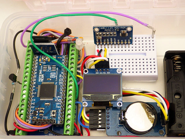
In this tutorial, a logger is built using a 3.3v Moteino MEGA with a 1284p CPU @ 16Mhz, w 4K eeprom,16K SRAM for variables & 128K program space. Considerably more than the 328’s 1K eeprom, 2K ram & 32K progmem. Also has a spare serial port for GPS/NEMA sensors.
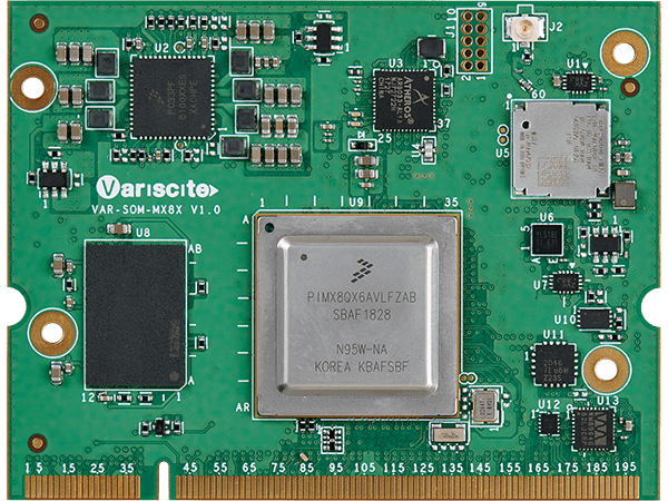
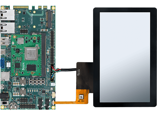
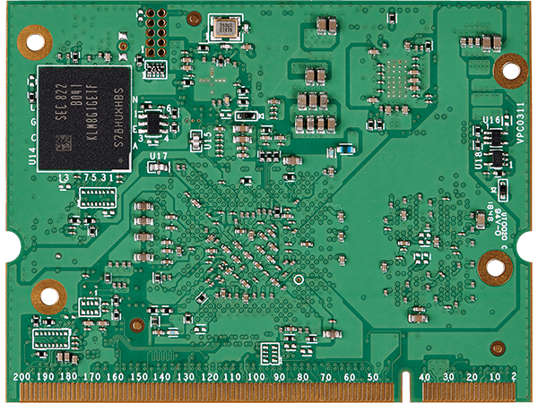
Variscite has re-launched its VAR-SOM-MX8X System on Module, based on the i.MX8X processor with the latest NXP’s qualified silicon for full production. The SoM expands Variscite’s VAR-SOM Pin2Pin product family and offers built-in safety features, highly integrated multimedia support, and efficient power/performance architecture.
Variscite, a System on Module global market leader and NXP’s partner, has re-launched its VAR-SOM-MX8X, an i.MX8X-based System on Module, with the latest i.MX8X silicon version for full production. Variscite’s launch takes place along with NXP’s formal broad market launch, following NXP’s introduction of the new silicon version earlier this quarter as the qualified revision for production. The VAR-SOM-MX8X has already been launched by Variscite last year and was available to Variscite’s early-access customers, allowing them to leverage the i.MX8X technology for new developments much earlier than the broad market launch.
The SoM expands the solutions range offered by the VAR-SOM Pin2Pin product family and provides a pin-compatible option to i.MX8, i.MX8M, i.MX8M Mini, i.MX8M Nano, i.MX6, i.MX6UL/ULL/ULZ and the upcoming i.MX8M Plus based modules. This extensive products family allows Variscite’s customers ultimate scalability, extended lifetime, and reduced development time, costs, and risk.
Product key features:
NXP iMX8X 1.2GHz Quad-Core Cortex-A35
Real-time 264MHz Cortex-M4F co-processor
Up to 4GB LPDDR4, 64GB eMMC
Integrated security and fail-safe features
2D/3D graphics acceleration
24-bit parallel LCD, LVDS/DSI
4K H.265 Decode, 1080p H.264 Encode/Decode
HQ audio in/out
Camera in: 1x MIPI-CSI2, 1x parallel CSI 8/10-bit
2x GbE, 2x USB 3.0, PCI-E
Analog input, CAN/CAN-FD, UART, SPI, I2C, SD/MMC, touch
Certified Wi-Fi 802.11 ac/a/b/g/n + BT4.2/BLE
Temperature range -40 to 85° C
OS: Linux, Android
Up to 15 years longevity
The VAR-SOM-MX8X is based on i.MX 8QuadXPlus / 8DualXPlus / 8DualX processor with up to Quad 1.2GHz Cortex-A35. Thanks to the integration of ARM’s most efficient Cortex-A35 cores with the Cortex-M4F real-time co-processor, the VAR-SOM-MX8X offers high processing capabilities in a power-optimized platform. In addition, the SoM provides a highly integrated solution with Vivante GC7000Lite GPU for 2D and 3D graphics acceleration, 4K H.265 Decode, 1080p H.264 Encode/Decode, Camera Interfaces, DSI / LVDS, Parallel LCD, dual GbE, certified Wi-Fi/BT, CAN/CAN-FD, USB3 and serial interfaces.
Availability and pricing
The VAR-SOM-MX8X System on Module and associated evaluation kits are available for orders in production quantities from only $79 per unit for 1Kpcs orders. Please contact Variscite’s Sales team for further details.
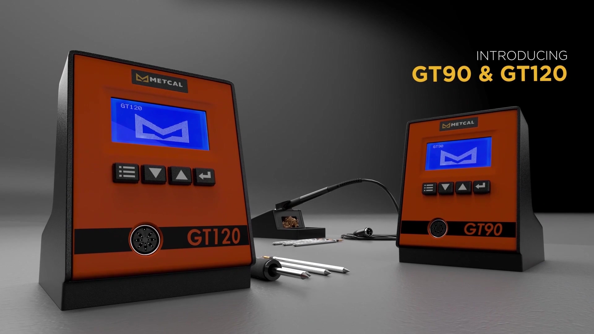
Metcal announced plans to launch its new GT90 and GT120 Soldering Systems. The GT90 and GT120 offer market-leading performance due to their use of inductive heating technology and are Metcal’s first platforms with adjustable temperature offered to the market.
The GT family of soldering systems are the only products in the market to offer the combination of inductive heating technology with adjustable temperature. This gives the GT systems a significant performance advantage with much faster time to temperature, thermal recovery and temperature stability during soldering over resistive heating systems offered by competitors in the same product category.
The GT90 is a single port soldering station, utilizing a 90-watt power supply and best-in-class performance vs. competitive 75-120-watt systems. It is compatible with Ultrafine and Standard tips and is ideal as a cost-effective solution for single iron applications on the production line.
The GT120 is a single port soldering station utilizing a 120-watt power supply and offers performance greater than competitive 150-200-watt systems and equivalent performance to much more expensive 250-watt systems. The GT120 is compatible with Ultrafine, Standard and High Thermal Demand tips and can be used for any type of single iron soldering application.
“With performance greater than anything offered in the market today, and the capability of handling the tiniest of components to the most demanding thermal load applications, the GT120 is the highest performing and most versatile soldering station available in the market today. It is ideal for production soldering, R&D labs, applications with extremely high thermal loads and soldering under a microscope.” said Joshua Edberg, Director of Marketing for Metcal.
Both units are supplied with an external power supply, allowing for a more compact design to save space on the bench, and improve the quality and life of the system. They also offer an intuitive user interface, password protected programs for temperature lockout and range selection, as well as a USB port to update software and power peripherals such as fans, lights, cameras or even a cell phone.
The complete system for each model includes a soldering station with an external power supply, one handpiece, and a work-stand to support a variety of soldering and rework applications using the associated tips and cartridges.
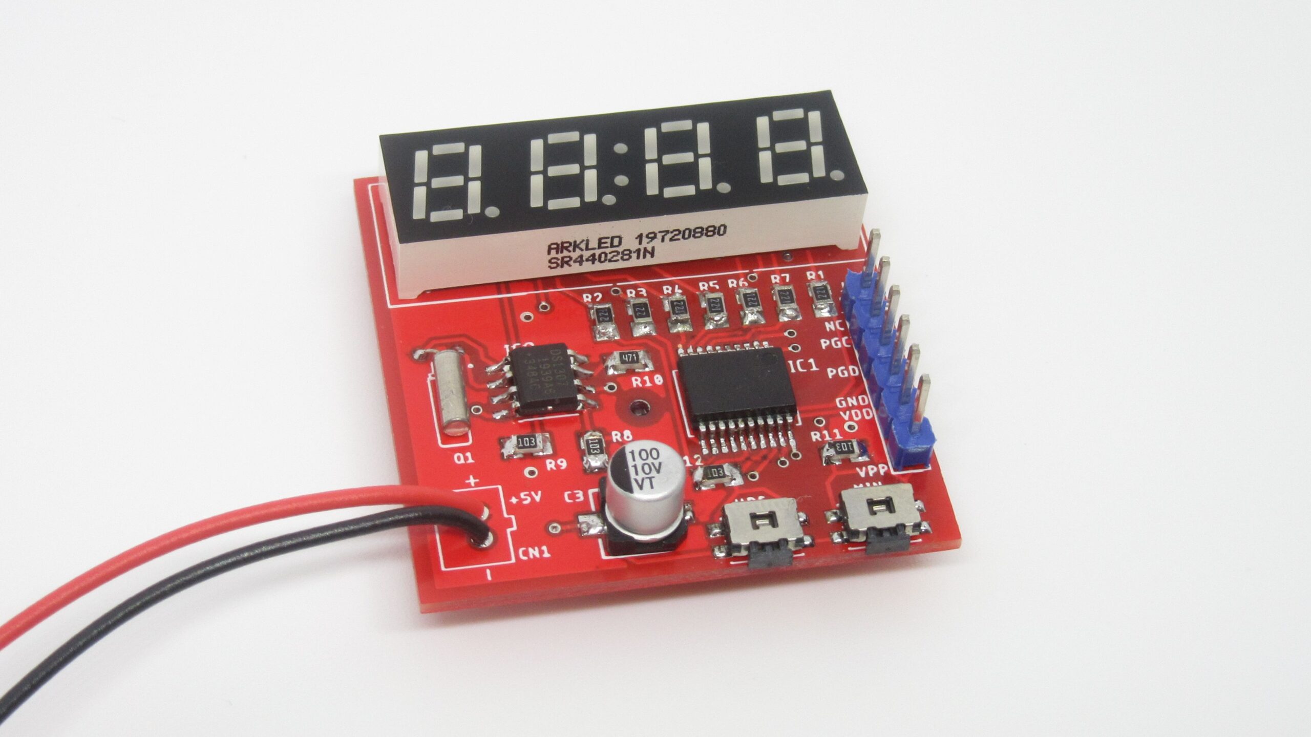
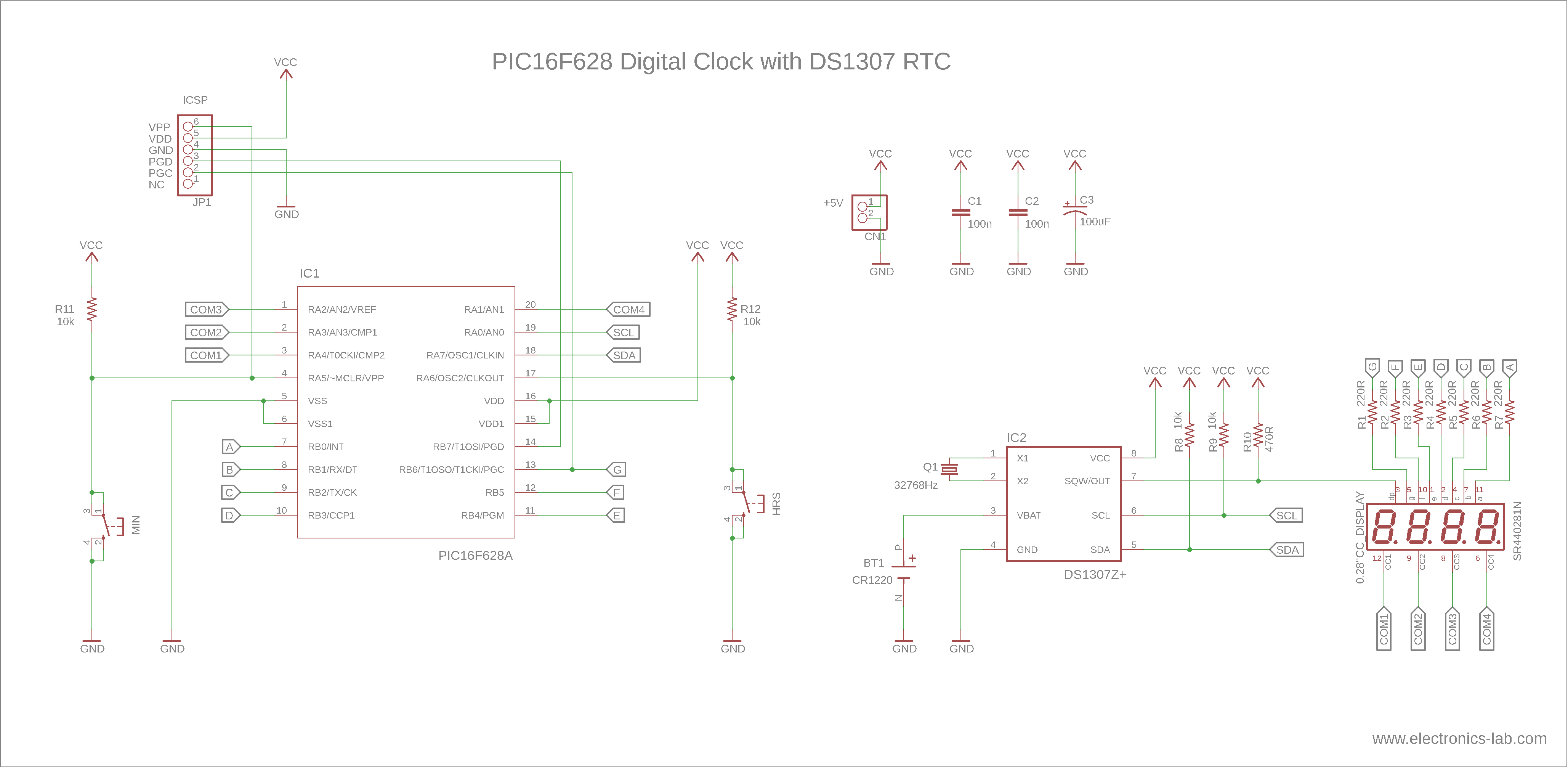
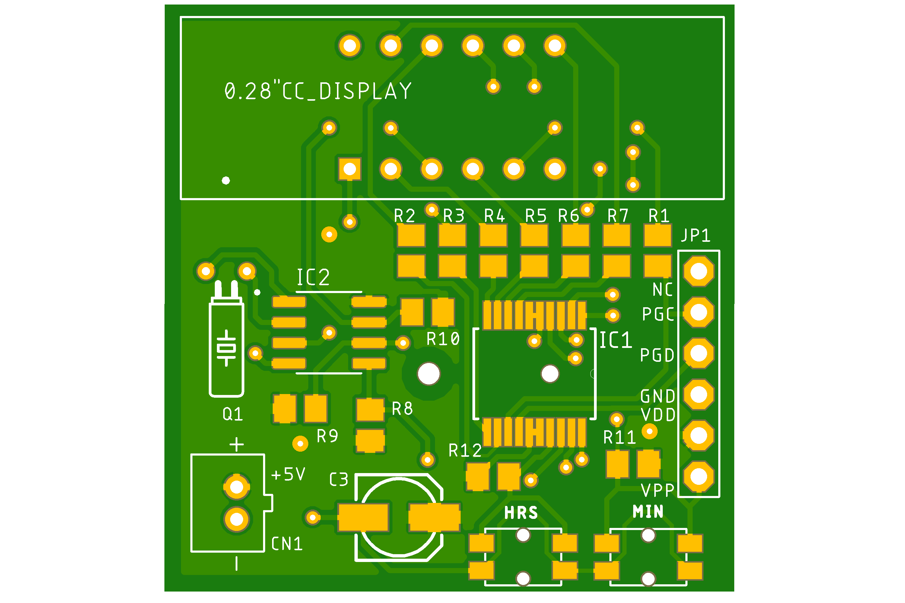
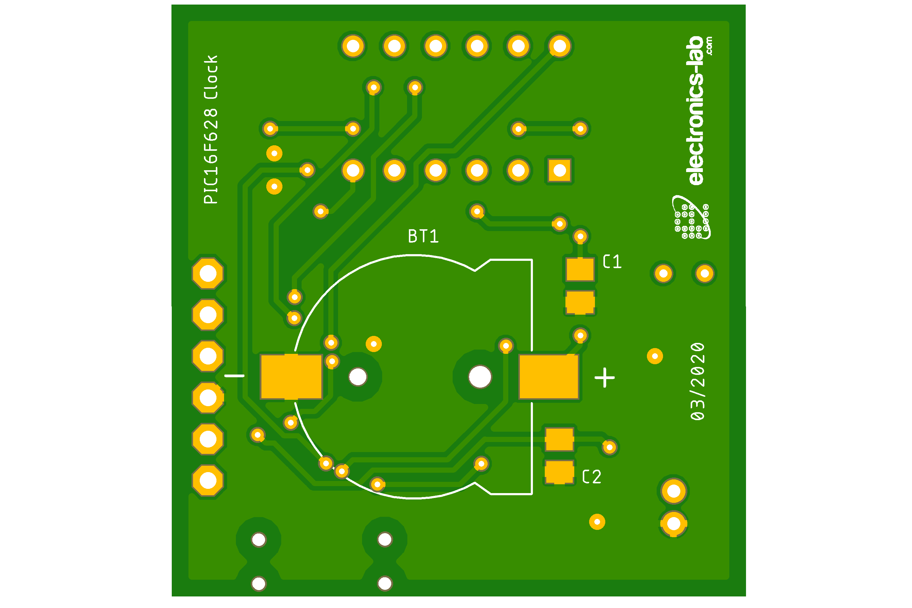
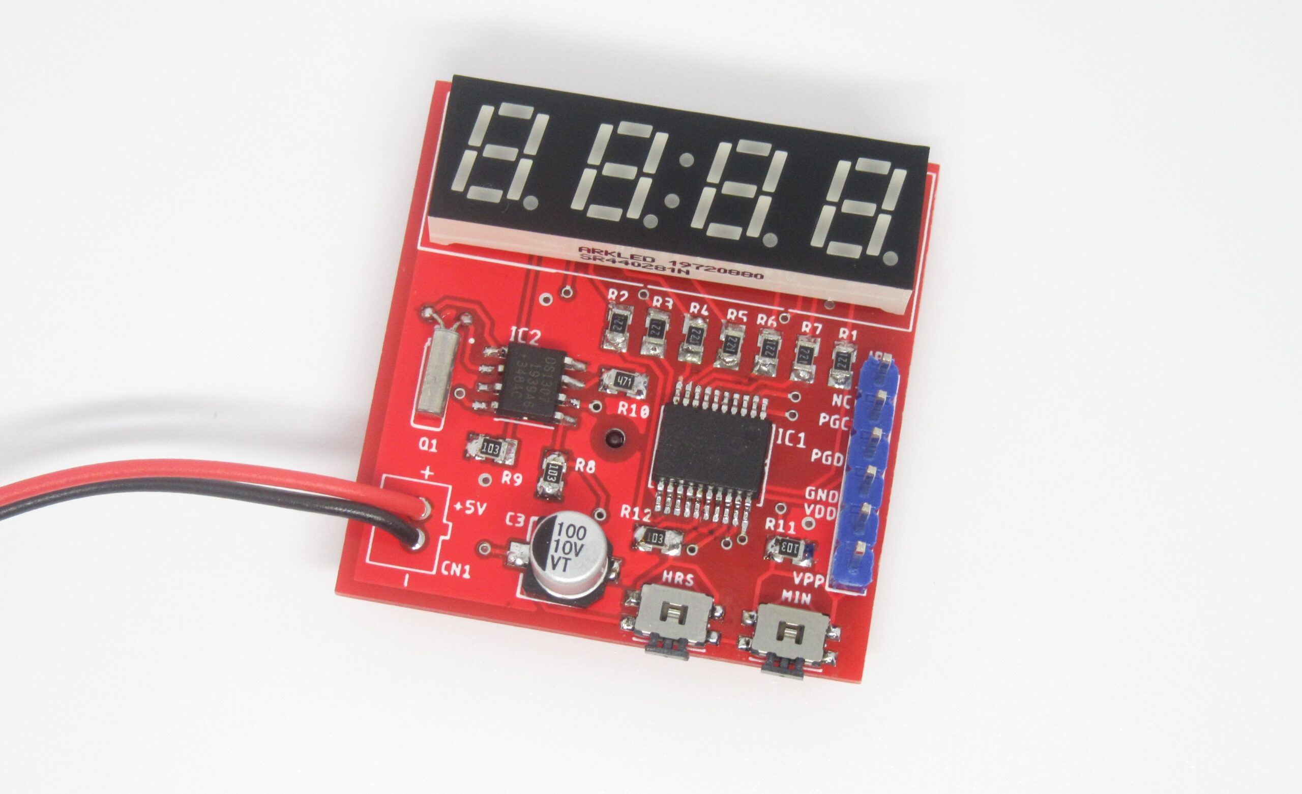
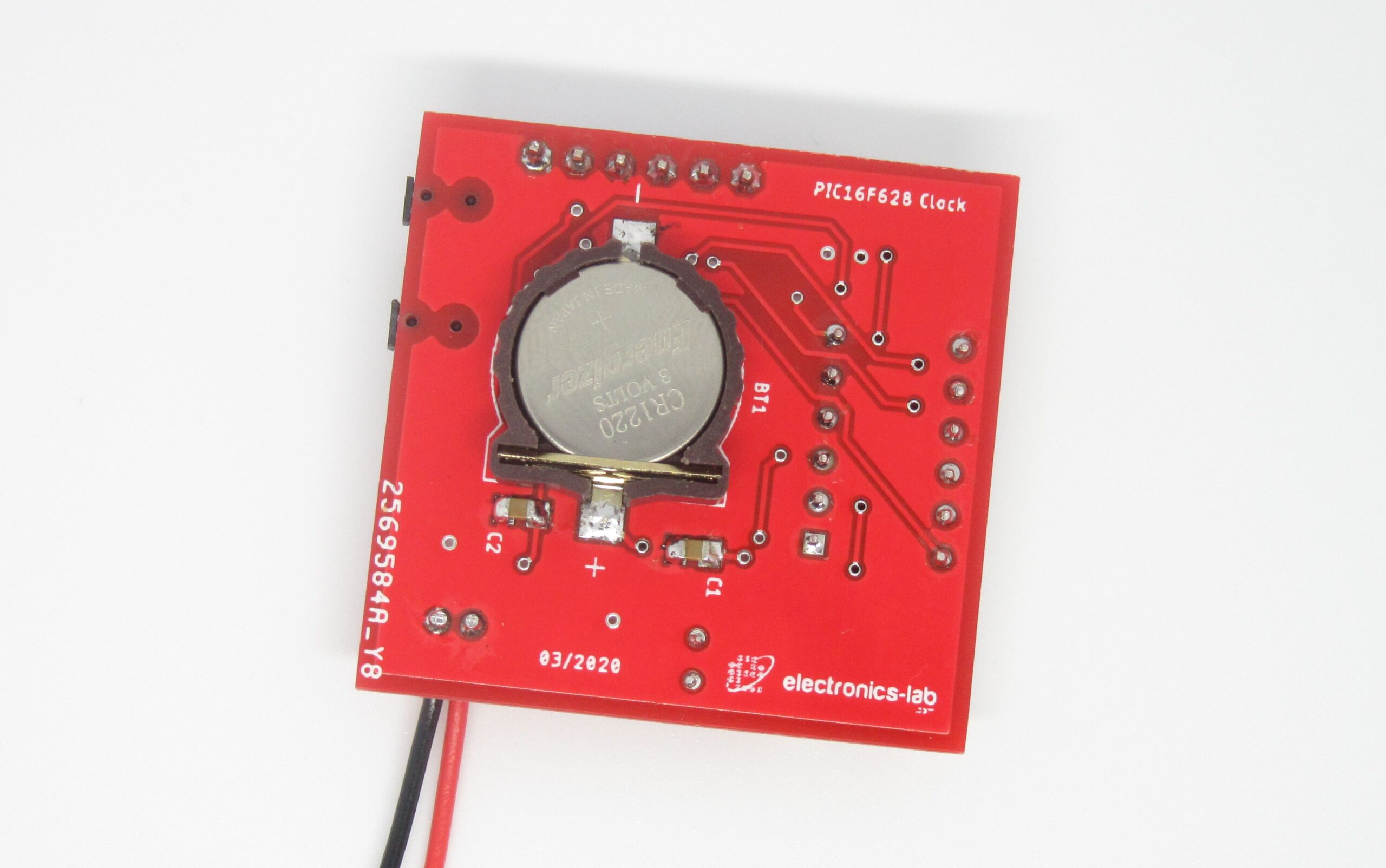
This is a minimal and small clock based on PIC16F628A microcontroller and DS1307 RTC IC. It is able to only show the time on a small 7-segment display with a total of 4 segments. The display we used is a 0.28″ SR440281N RED common cathode display bought from LCSC.com, but you can use other displays as well such as the 0.56″ Kingbright CC56-21SRWA. This project is heavily inspired by the “Simple Digital Clock with PIC16F628A and DS1307” in the case of schematic and we also used the same .hex as”Christo”.
Schematic
The schematic is straight forward. The heart is the PIC16F628A microcontroller running on the internal 4MHz oscillator, so no external crystal is needed. This saves us 2 additional IOs. The RESET Pin (MCLR) is also used as input for one of the buttons. All display segments are connected to PORTB and COMs are connected to PORTA. The RTC chip is also connected to PORTA using the I2C bus.
The refresh rate of the digits is about 53Hz and there is no visible flickering. The display segments are time-multiplexed and this makes them appear dimmer than the specifications. To compensate we are going to use some low resistors on the anodes. “Christo” tested it with different values for current limiting resistors R1-R7 and below 220Ω the microcontroller starts to misbehave (some of the digits start to flicker) above 220 Ohm everything seems OK. On the display we used the two middle dots are not connected to any pin on the package, so for the seconds’ indicators, we used the “comma” dots. These pins are connected to the SQW pin of the DS1307, which provides a square wave output with 1 sec period. The SQW pin is open drain, so we need to add a pull-up resistor. Τhe value of this resistor is chosen at 470Ω, after some trial and error testing. On the input side of the MCU, there are two buttons for adjusting the MINUTES and HOURS of the clock as indicated on the schematic. Onboard there is also an ICSP Programming connector, to help with the firmware upload. Finally, there is one unused pin left (RB7), which can be used for additional functionality, like adding a buzzer or an additional LED.
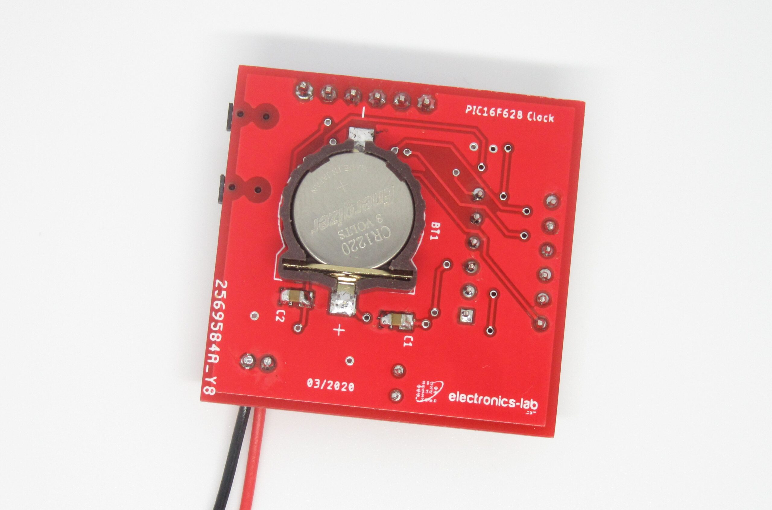
The DS1307 RTC needs an external crystal to keep the internal clock running and a backup battery to keep it running while the main power is OFF. So, the next time you power ON the clock the time would be current. To keep the overall board dimensions small we used a CR1220 battery holder with the appropriate 3V battery. Power consumption is about 35-40mA @ 5V input.
Code
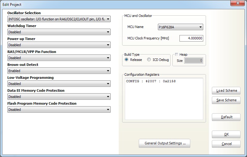
According to the author, the code is written and compiled with MikroC Pro and uses the build-in software I2C library for communicating with RTC chip. If you want to use MPLAB IDE for compiling the code you should write your own I2C library from scratch. For programming the board we used PICkit 3 programmer and software. In this case, in the “Tools” menu check the option “Use VPP First Program Entry“.
PIC Programmer Configuration
The code for this project is listed below. Additionally, you will need the “Digital Clock (PIC16F628A, DS1307, v2).h” file which can be found on the .zip in downloads below. Compiled .hex file is also provided on the same .zip file.
#include "Digital Clock (PIC16F628A, DS1307, v2).h"
#define b1 RA6_bit
#define b2 RA5_bit

// b1_old, b2_old - old state of button pins
// hour10, hour1 - tens and ones of the hour
// min10, min1 = tens and ones of the minutes
byte b1_old, b2_old, hour1, hour10, min1, min10;

// definitions for Software_I2C library
sbit Soft_I2C_Scl           at RA0_bit;
sbit Soft_I2C_Sda           at RA7_bit;
sbit Soft_I2C_Scl_Direction at TRISA0_bit;
sbit Soft_I2C_Sda_Direction at TRISA7_bit;


//  correct bits for each digit
//     RB6 RB5 RB4 RB3 RB2 RB1 RB0
//     g   f   e   d   c   b   a
//  0: 0   1   1   1   1   1   1   0x3F
//  1: 0   0   0   0   1   1   0   0x06
//  2: 1   0   1   1   0   1   1   0x5B
//  3: 1   0   0   1   1   1   1   0x4F
//  4: 1   1   0   0   1   1   0   0x66
//  5: 1   1   0   1   1   0   1   0x6D
//  6: 1   1   1   1   1   0   1   0x7D
//  7: 0   0   0   0   1   1   1   0x07
//  8: 1   1   1   1   1   1   1   0x7F
//  9: 1   1   0   1   1   1   1   0x6F
// BL: 0   0   0   0   0   0   0   0x00

const byte segments[11] = {0x3F, 0x06, 0x5B, 0x4F, 0x66, 0x6D, 0x7D, 0x07, 0x7F, 0x6F, 0x00};


//***********************************************//
//   Sets read or write mode at select address   //
//***********************************************//
void DS1307_Select(byte Read, byte address) {
     Soft_I2C_Start();
     Soft_I2C_Write(0xD0);       // start write mode
     Soft_I2C_Write(address);    // write the initial address
     if (Read) {
        Soft_I2C_Stop();
        Soft_I2C_Start();
        Soft_I2C_Write(0xD1);    // start read mode
     }
}

//********************************//
//   Initialize the DS1307 chip   //
//********************************//
void DS1307_Init() {
     byte sec, m, h;
     DS1307_Select(1, 0);                 // start reading at address 0
     sec = Soft_I2C_Read(1);              // read seconds byte
     m = Soft_I2C_Read(1);                // read minute byte
     h = Soft_I2C_Read(0);                // read hour byte
     Soft_I2C_Stop();
     if (sec > 127) {                     // if the clock is not running  (bit 7 == 1)
        DS1307_Select(0, 0);              // start writing at address 0
        Soft_I2C_Write(0);                // start the clock (bit 7 = 0)
        Soft_I2C_Stop();
        DS1307_Select(0, 7);              // start writing at address 7
        Soft_I2C_Write(0b00010000);       // enable square wave output 1 Hz
        Soft_I2C_Stop();
     }
     m = (m >> 4)*10 + (m & 0b00001111);  // converting from BCD format to decimal
     if (m > 59) {
        DS1307_Select(0, 1);              // start writing at address 1
        Soft_I2C_Write(0);                // reset the minutes to 0
        Soft_I2C_Stop();
     }
     if (h & 0b01000000) {                // if 12h mode (bit 6 == 1)
        if (h & 0b00100000)               // if PM (bit 5 == 1)
           h = 12 + ((h >> 4) & 1)*10 + (h & 0b00001111);
        else
           h = ((h >> 4) & 1)*10 + (h & 0b00001111);
     }
     else
        h = ((h >> 4) & 3)*10 + (h & 0b00001111);
     if (h > 23) {
        DS1307_Select(0, 2);              // start writing at address 2
        Soft_I2C_Write(0);                // reset the hours to 0 in 24h mode
        Soft_I2C_Stop();
     }
}


void incrementH() {     // increments hours and write it to DS1307
     hour1++;
     if ((hour10 < 2 && hour1 > 9) || (hour10 == 2 && hour1 > 3)) {
        hour1 = 0;
        hour10++;
        if (hour10 > 2)
           hour10 = 0;
     }
     DS1307_Select(0, 2);
     Soft_I2C_Write((hour10 << 4) + hour1);
     Soft_I2C_Stop();
}


void incrementM() {     // increments minutes and write it to DS1307
     min1++;
     if (min1 > 9) {
        min1 = 0;
        min10++;
        if (min10 > 5)
           min10 = 0;
     }
     DS1307_Select(0, 0);
     Soft_I2C_Write(0);                       // reset seconds to 0
     Soft_I2C_Write((min10 << 4) + min1);     // write minutes
     Soft_I2C_Stop();
}

void main(){
     // pos: current digit position;
     // counter1, counter2: used as flag and for repeat functionality for the buttons
     // COM[]: drive the common pins for the LED display
     byte pos, counter1, counter2, COM[4] = {0b11101111, 0b11110111, 0b11111011, 0b11111101};
     CMCON = 0b00000111;             // comparator off
     TRISA = 0b01100000;
     TRISB = 0b00000000;
     b1_old = 1;
     b2_old = 1;
     counter1 = 0;
     counter2 = 0;
     pos = 0;
     Soft_I2C_Init();
     DS1307_Init();
     while (1) {
           DS1307_Select(1, 1);      // select reading at address 1
           min1 = Soft_I2C_Read(1);  // read minutes byte
           hour1 = Soft_I2C_Read(0); // read houts byte
           Soft_I2C_Stop();
           min10 = min1 >> 4;
           min1 = min1 & 0b00001111;
           hour10 = hour1 >> 4;
           hour1 = hour1 & 0b00001111;
           if (b1 != b1_old) {        // if the button1 is pressed or released
              b1_old = b1;
              counter1 = 0;
           }
           if (!b1_old) {             // if the button1 is pressed
              if (counter1 == 0)
                 incrementH();        // increment hour
              counter1++;
              if (counter1 > 50)      // this is repeat functionality for the button1
                 counter1 = 0;
           }
           if (b2 != b2_old) {        // if the button2 is pressed or released
              b2_old = b2;
              counter2 = 0;
           }
           if (!b2_old) {             // if the button2 is pressed
              if (counter2 == 0)
                 incrementM();        // increment minutes and reset the seconds to 0
              counter2++;
              if (counter2 > 50)      // this is repeat functionality for the button2
                 counter2 = 0;
           }

           TRISA = TRISA | 0b00011110;       // set all 4 pins as inputs
           switch (pos) {                    // set proper segments high
             case 0: PORTB = segments[hour10]; break;
             case 1: PORTB = segments[hour1]; break;
             case 2: PORTB = segments[min10]; break;
             case 3: PORTB = segments[min1]; break;
           }
           TRISA = TRISA & COM[pos];         // set pin at current position as output
           PORTA = PORTA & COM[pos];         // set pin at current position low
           pos++;                            // move to next position
           if (pos > 3) pos = 0;
     }
}
PCB
PCB is designed with Autodesk EAGLE and design files are available in downloads below. The overall dimensions of the board are 35.56 x 36.61 mm and we used almost SMD components.
Spare PCBs are available for shipment around the world. If you would like to get some drop us a line.
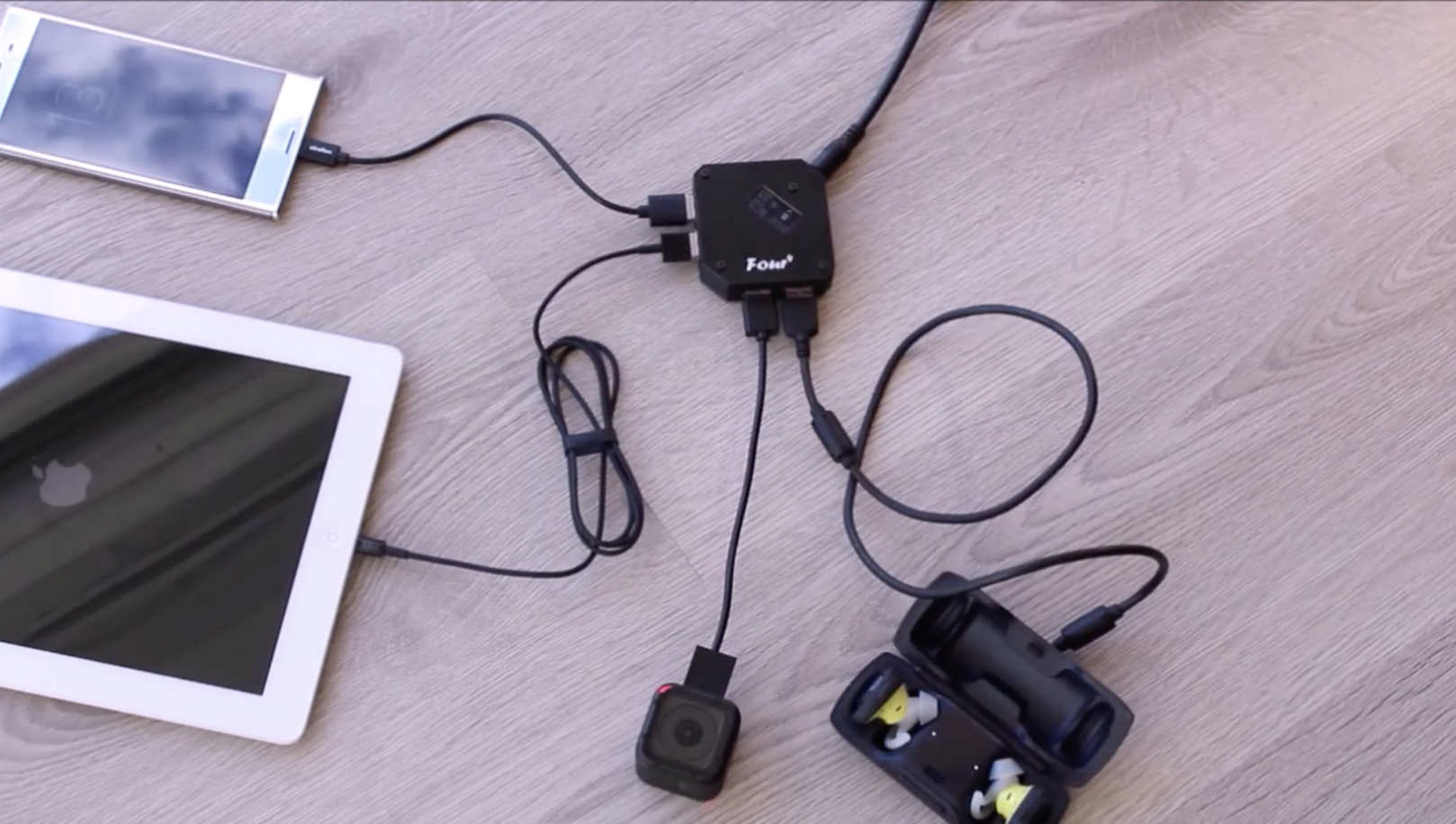
The more the electronic devices to charge, the more the multiple-port USB chargers to have, especially intelligent ones!
Yes, charging multiple devices at the same time can be very tiring; from having to deal with the mess of the plenty of cables and adapters needed for the different devices to hunting for free wall sockets and then to the inconveniences faced when trying to charge on a journey. But with multi-port USB chargers, things have really become much easier and faster!! However, while it seems like some have been able to fully satisfy the needs of people, others have not.
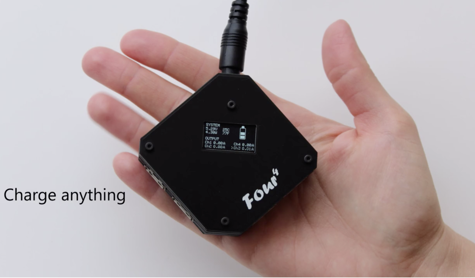
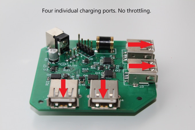
“The main reason the idea was brought to life is that I have never been satisfied with multi-port chargers. They are built with cheap components and lack functions that I believe are prerequisites for safe and smart charging. Many of them are told to deliver high power but when they are put to the feat, many of them fail in different aspects. Throttling the power outputs is most common, overheating or having very high voltage ripple are issues often found”, says Karoly Simon, Sweden-based designer of the Four4 multiple-port USB charger.
The Four4 USB charger design offers safety functions including data integrity protection that protects devices from data intrusion and harmful spyware when used in public USB outlets. The charger also has an OLED display that shows important system information as well as charging performance for charging optimization. All the channels of the charger are independent and each optimizes charging current to be as high as possible.
The Four4 is a perfect power supply for most SBCs too; its 3.2 power supply mode can satisfy the most power demanding board without disruption. Charger Specifications include:
Input Voltage: 4.7 – 5.5V
Output voltage: 5.3V
Output current for each port: 8A
Dimension: 60 x 60 x 21 mm (2.4 x 2.4 x 0.83 inch)
Weight: 60 grams
Simon adds that measurements, specifications, and results regarding safety functions, current supply, and power are however valid only with bundled power supply.
“You can use any 5V PSU to power the Four4 but minimum 5V/4A is recommended. To utilize/deliver the full 40W, you need to connect a minimum 5V/8A PSU!!”
More details on the Four4 multiple-port USB charger are available on IndieGoGo where it was launched with a $33,000 funding goal, and shipping scheduled to start in November 2020.
Arrow Electronics, Panasonic Industry, and STMicroelectronics (ST) have introduced a low-power wireless multi-sensor edge-intelligence solution for smart factory, smart home, and smart life applications.
The IoT Solution Module combines Arrow’s engineering and global distribution capabilities with Panasonic Industry’s IoT modules based on the ST BlueTile (STEVAL-BCN002V1B) multi-sensor development kit. This combination enables customers to test their ideas easily and bring new IoT products to the market faster.
The IoT Solution Module features ST’s latest BlueNRG Bluetooth Low Energy (BLE) 5.0 system-on-chip (SoC) paired with numerous inertial, environmental, and audio sensors. The onboard sensors enable the cost-effective delivery of a broad range of compact and valuable IoT applications for smart factory, smart home and smart life scenarios.
Comprehensive services and validation processes enable a reduced BOM that combines an accelerometer and gyroscope with Time-of-Flight, pressure, and humidity sensors in an efficient low-power design with Bluetooth communications. This combination enables OEM customers to dramatically slash time-to-market and reduce design expense and complexity using certified modules.
“Building on the outstanding features and design of the ST BlueTile sensor-node development kit, the modules now available from Panasonic Industry through Arrow Electronics are ideal for speeding creation of a wide range of edge-node sensors for all kinds of Internet-of-Things applications,” said Philip Lolies, EMEA Vice President, Marketing & Application, STMicroelectronics.
”Panasonic’s IoT Solution Modules inspired by ST BlueTile support customers by cutting down their time to market in this fast paced era”, said Dr. Sara Ghaemi, Team Leader, IoT, Panasonic Industry Europe GmbH. “Panasonic Industry is able to offer an unrivaled customer service throughout all stages of the product lifecycle ranging from design, development and validation to aftermarket. The modules support customers in reducing their development efforts and overall product costs while guaranteeing the highest quality and required certifications. This new solution will serve the customer’s needs in smart factory, smart home and smart life applications.”
“The modern embedded design requires sensors and wireless connectivity. This is accelerating based on the breadth of wireless standards being integrated into products,” said Matthias Hutter, Vice President, Product Management and Supplier Marketing, Arrow Electronics, EMEA. “However, using sensors and designing the supporting circuitry for the task would take a lot of time and resources to develop. Additional certification time is needed on top. Using pre-qualified wireless sensor modules in the system design is saving development time and budget which speeds up time to market for our customers. By working with ST and Panasonic we are bringing the fundamental sensor and wireless building blocks in a great package for accelerated design.”
New tool, ‘Code Defect AI,’ allows earlier discovery of bugs, minimizing the cost to fix them and speeding up the development cycle.
Altran, the global leader in engineering and R&D services, today announced the release of a new tool available on GitHub that predicts the likelihood of bugs in source code created by developers early in the software development process. By applying machine learning (ML) to historical data, the tool – called “Code Defect AI” – identifies areas of the code that are potentially buggy and then suggests a set of tests to diagnose and fix the flaws, resulting in higher-quality software and faster development times.
Bugs are a fact of life in software development. The later a defect is found in the development lifecycle, the higher the cost of fixing a bug. This bug-deployment-analysis-fix process is time consuming and costly. Code Defect AI allows earlier discovery of defects, minimizing the cost of fixing them and speeding the development cycle.
“It’s well known that software developers are under constant pressure to release code fast without compromising on quality,” said Walid Negm, Group Chief Innovation Officer at Altran. “The reality however is that the software release cycle needs more than automation of assembly and delivery activities. It needs algorithms that can help make strategic judgments ‒ especially as code gets more complex. Code Defect AI does exactly that.”
Code Defect AI relies on various ML techniques including random decision forests, support vector machines, multilayer perceptron (MLP) and logistic regression. Historical data is extracted, pre-processed and labelled to train the algorithm and curate a reliable decision model. Developers are given a confidence score that predicts whether the code is compliant or presents the risk of containing bugs.
Code Defect AI supports integration with third-party analysis tools and can itself help identify bugs in a given program code. Additionally, the Code Defect AI tool allows developers to assess which features in the code have higher weightage in terms of bug prediction, i.e., if there are two features in the software that play a role in the assessment of a probable bug, which feature will take precedence.
“Microsoft and Altran have been working together to improve the software development cycle, and Code Defect AI, powered by Microsoft Azure, is an innovative tool that can help software developers through the use of machine learning,” said David Carmona, General Manager of AI Marketing at Microsoft.
Code Defect AI is a scalable solution that can be hosted on premise as well as on cloud computing platforms such as Microsoft Azure. While the solution currently supports GitHub, which is owned by Microsoft, it can be integrated with other source-code management tools as needed.
The tool is also available on the Microsoft AI Lab portal so that Microsoft developers can download the solution and use it internally.