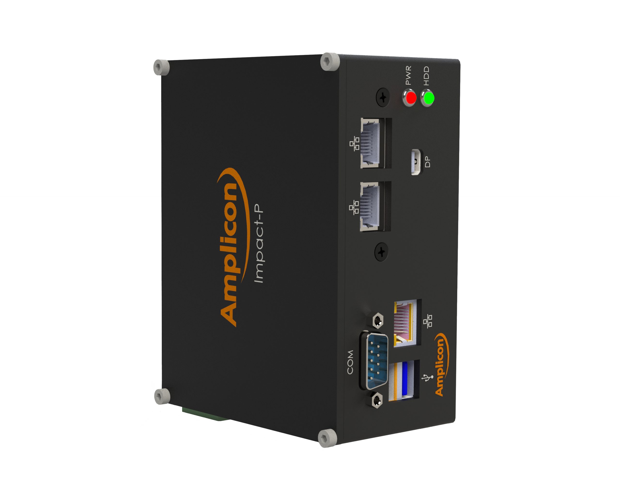
DINrail-mountable Impact-P series are ultra-compact 4.7” x 2.2” x 3.8” Intel® ATOM™-based embedded PCs: low-current, 9-36V operation, fanless design, customizable, with long life cycle.
Saelig Company, Inc. (www.saelig.com) announces what is probably the smallest industrial embedded PC in the marketplace, the Amplicon Impact-P Series. These rugged PCs feature the Intel® Apollo Lake ATOM™ E3900 generation processors, supported by high bandwidth DDR3L 1600MHz memory, in an ultra-compact (4.7” x 2.2” x 3.8”) housing that is milled out of solid aluminum. This makes these units ideal for applications in harsh conditions where space and power is at a premium.
The tiny Impact-P is a fanless, DINrail-mountable, low power embedded system, which has been designed to provide convenience and versatility, with a unique set of features that are unusual in an industrial PC of miniature size.
Standard specs include:
Intel Atom® x5-E3930 Dual Core Processor with 2M cache, 1.3GHz (1.8GHz), 6.5W 2GB DDR3L (max 8GB) LAN: 1 x Intel® 10/100/1000 network connection (supports PXE and WoL) 2 x 10/100/1000 POE+ LAN (IEEE 802.3at, up to 25.5W) with 64GB SSD storage.
Expansion: 1 x Full-size Mini PCIe (PCIe/USB 2.0) 1 x M.2 B key 2242. (PCIe/USB 2.0/SATA 3.0)
External Interfaces: 1 x DP++ 2 x USB 3.0 1 x RS232/422/485 1 x Intel® GbE RJ45 (I211AT) 2 x Isolated POE+ LAN (max 25.5W per port)
The Impact-P’s specified operating temperature range is from -20degC to 70degC, with wide temperature RAM and SSD in the design. The system can be fully customized, with selections that include +9 to 36VDC or POE powered, Dual POE+, multiple I/O configurations, custom branding, chassis color, etc. OS support includes Linux, Windows 10, and Windows 10 IoT.
The Impact-P range of embedded PC’s is suited to low power applications such as transport, utilities and security, and situations requiring offsite connectivity or remote operation. The unit can also be manufactured in custom dress for uniformity with a company’s other branded OEM products. With an extremely compact design and weighing less than 2lbs, this embedded controller is ideal for any installation where space is severely limited. Made by Amplicon, the UK market-leading manufacturer of industrial computers, the Impact-P embedded PC system is available now from Saelig Company, Inc., Amplicon’s USA technical distributor.
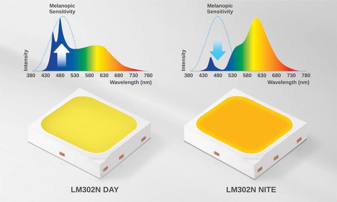
Lighting to energize or relax: new LED packages help improve alertness and the quality of sleep by adjusting melatonin levels.
Samsung Electronics unveiled its first “human-centric” LED packages, collectively known as LM302N. Engineered with carefully created light spectra, the LM302N family helps human bodies adjust melatonin levels indoors, making people feel more energetic or relaxed depending on their daily life patterns.
Melatonin, a hormone that regulates the sleep-wake cycle, responds to the cyan wavelength range of light. Brighter cyan-concentrated lighting suppresses the body’s production of melatonin, increasing concentration and enabling a greater overall sense of alertness. Similarly, a lower cyan light intensity minimizes disturbances to the natural onset of the body’s melatonin production, helping to promote sleep quality.
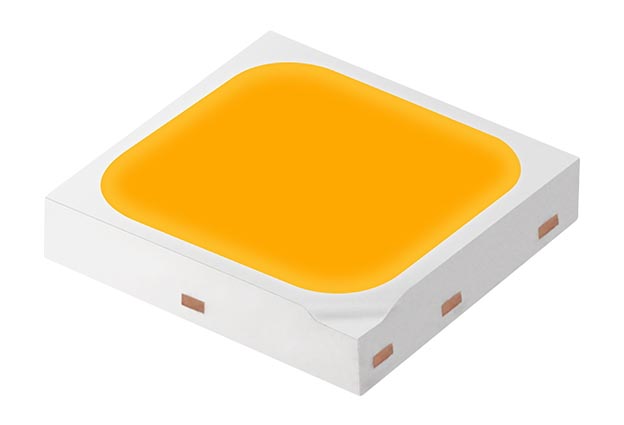
Samsung’s LM302N utilizes precisely designed light spectra with optimized amounts of cyan to accommodate the lighting needs to the extent desired at any given point in time: the LM302N DAY improves alertness and the LM302N NITE enhances relaxation. Standardized at 3.0 × 3.0 mm, these offerings can fit in a wide range of lighting fixtures and are protected against humidity and heat.
The LM302N DAY can suppress the body’s melatonin level more than 18 percent below that of conventional LED lighting. Available in a variety of color temperatures from 3000K to 6500K, the DAY package can be used in a diverse range of indoor applications, such as schools, offices, libraries and industrial sites, to enhance an individual’s sense of awakeness and energy level.
The LM302N NITE can provide a proper level of brightness without hindering the release of melatonin, helping people to maintain the hormone level as if they were in a calm natural atmosphere at night. The body releases about five percent more melatonin under lights with the LM302N NITE packages than conventional LED packages, increasing relaxation. By comparison, spending a lot of time under conventional nighttime lighting can cause excessive alertness that makes it harder to fall asleep. Additionally, the LM302N NITE is offered in color temperatures between 1800K and 4000K, providing design flexibility to bring the benefits of relaxing light to a variety of lighting spaces.
The DAY and NITE packages can also be combined into a single luminaire to help people maintain their natural circadian rhythm 24 hours a day. This duo-lighting option is optimal for those who spend most of their time indoors and struggle with confused body clocks.
The newly launched LM302N family is now in mass production.
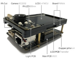
Sochip partners with Allwinner to launch a new V831 development board that showcases an Allwinner V831 IP Camera SoC, the very first to include an AI chip.
Allwinner has released quite a number of camera processors in the past, the V3, V316, S3, and many more, but none of them ever came with a built-in NPU aka AI accelerator. Things, however, have taken a new turn now as an Allwinner V831 AI full HD Camera SoC with NPU aka AI accelerator is used to power Sochip’s linux-driven V831 development board.
Allwinner’s high performance, low powered IP camera SoC integrates single-core ARM Cortex-A7 topping out at 800MHz frequency and supports H.265 video encoding of multiple streams up to 1080p @ 330fps. The SoC also features a 0.2 TOPS NPU for facial recognition and detection, Electronic image stabilization engine support, the latest generation of ISP image processor that supports up to 2688 x 2688 pixels, wide-angle distortion correction, PTZ calibration, SmartColor support for excellent display and other image correction algorithms that make it easy to achieve professional image effects.
It is further equipped with 20-bit audio codec for audio input and output, crypto engine, 64MB DDR2, external eMMC 5.0 interface, NOR and SPI NAND flash.
Other features include:
2-lane MIPI-CSI interface
RGB output up to 320 x 240 @ 60fps
10/100 Mbps Ethernet port
TDM interface for connecting to external audio codec
Up to 54 GPIOs
USB 2.0 OTG
4x UART
12S
SPI
1x RTC
Dimension: 9 x 9 mm
Supply voltage: Core: 0.9V, I/O: 3.3V
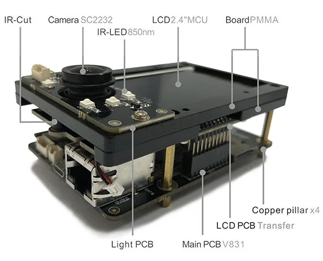
Meanwhile, the 280 x 200 x 180 mm V831 development board consists of four parts: the main PCB powered by an Allwinner V831 processor, camera board, 2.4 inch LCD display and a “light” PCB with IR receiver that has a 2-megapixel image sensor for superior low-light performance. There is no mention of storage, so the board probably relies on the 64MB DDR2 RAM of the V831 SoC.
The V831 kit sells for $440 on Alibaba (shipping included) but there is no known price concerning the V831 IP Camera SoC. The board is targeted at those planning to design AI-enabled IP cameras with AI features while the Allwinner V31 SoC is useful for applications like security monitoring, driving recorders, switched digital video, and body-worn police cameras.
More details can be found on the V831 SoC wiki page.
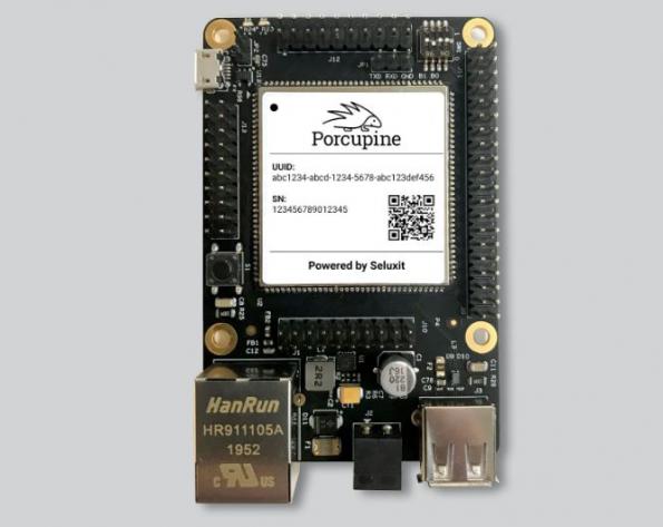
Seluxit has released IoT rapid prototyping kits based on it’s single-board computer, SLXPorcupine. If you have a smartphone, an internet connection and Seluxit’s IoT rapid-prototyping solution, then 10 minutes is all you need to create IoT prototypes that feel at home even in industrial settings. By julien happich @ eenewseurope.com
Claiming your device is as seamless as scanning a QR code, and adding plug-and-play sensors can now be done by using a wizard and hitting a “deploy” button. SLX Porcupine is an industrial-grade, single-board computer with a Raspberry Pi compatible form factor,running Linux. That makes it possible to use hats and open-source code from the Raspberry Picommunity. SLX Porcupine automatically connects to Viasens by Seluxit; a cloud-based, secure IoT Infrastructure.
Viasens has secure connectivity, over-the-air firmware update, and a configurable dashboard where you can see and analyse your data. Viasens also features data logging and extraction, reference code for your own iOS and Android native applications, as well as web interfaces. The SBC features a 4GB on-board flash and 512 MB RAM.
It also has 3 additional 20-pin headers, featuring functionalities such as Modbus, CAN bus and up to 8 channels of 12 bit ADCs. It can handle the temperature range often required in an industrial setting, from -40 to +85°C. Secure boot effectively prevents tampering on the device.
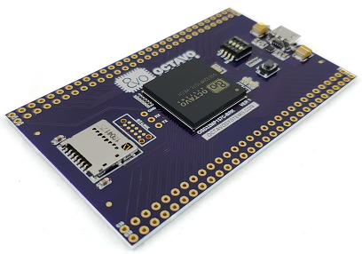
The OSD32MP1-BRK is a small flexible prototyping platform for the STM32MP1 based SiP, the OSD32MP15x. At only 3in X 1.8in (75mm X 46mm), it provides easy access to the I/O of the STM32MP1 through a set of breadboard compatible headers. The OSD32MP1-BRK allows developers to quickly build a proof of concept that more closely resembles their actual system without the need to build their own custom hardware.
The OSD32MP1-BRK features the OSD32MP15x System in Package, a microSD slot, 32KHz crystal, a microUSB client port, and two 2×30 100 mill headers. The headers give access to 106 I/O on the STM32MP1 integrated into the OSD32MP15x SiP. It is uses a 4 Layer PCB with low cost design rules and has no back side components.
Its minimal overhead and access to a wide range of I/O make the OSD32MP1-BRK the perfect platform for any designer looking for complete flexibility as they prototype their design.
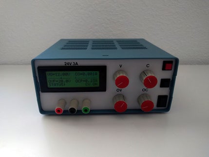
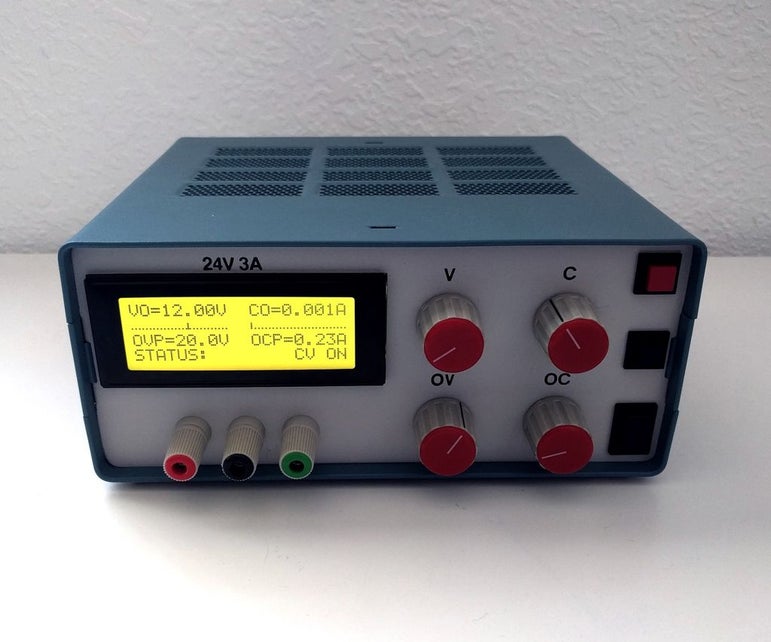
I have always believed that one of the best things about being a maker, is the ability to build your own tools, and we have covered the development of several tools like this in the past. For today’s tutorial, we will add another tool to the list, as I will be sharing a guide on how you can build a robust, fully-functional, Lab Bench Power Supply.
As with most tools, there are several DIY guides on the internet, but for today’s tutorial, I will be share how to build the “Super Lab Power Supply” built by “Danielrp“. Just like his LiPo battery tester which we covered a while back, the Super Lab Power supply comes in a beautiful enclosure that takes into account the importance of functionality without compromising aesthetics.
Highlight features of the superb lab power supply include:
Nominal Voltage: 24V.
Nominal Current: 3A.
Output Voltage Ripple: 0.01% (According to the specs of the power supply circuit kit).
Voltage measurement resolution: 10mV.
Current measurement resolution: 1mA.
CV and CC modes.
Over-current protection.
Overvoltage protection.
The SuperLab Power Supply is based on the super cheap VkMaker adjustable DC regulated power supply DIY module being sold on eBay. The power supply, which comes as a kit with THT type components and a PCB (so its easy to solder), takes in 24V AC supply at its input and gives between 0-30V at its output depending on user input via an onboard potentiometer. The module is able to supply up to 3A current and is equipped with safety features that help prevent overload and shorts.
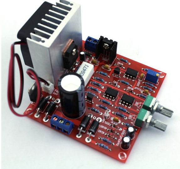
While the module had all that is needed to regulate and vary the voltage/current, it lacks feedback features that could make it more useful. For example, unless you connect a voltmeter/ammeter to the output terminals, there is no feedback to know what effects turning the potentiometer has on the output. To provide this desired feedback and other features in a digital and neat way, Daniel developed a metering circuit based on an Arduino Uno. The metering circuit, which is designed as an Arduino Shield, sits in-between the output of the VKmaker PSU and the load, measuring the voltage and current at the output of the Vkmaker PSU and displaying it in an innovative way on a 20×4 LCD.
Asides monitoring the voltage and current, the metering circuit also includes pushbuttons that are used to turn the device “ON” or “OFF”, along with a few additional potentiometers which can be used in setting the point at which the device initiates overvoltage and overcurrent protection among others. All of these features helps ensure you can safely power devices for tests in the lab without worrying about possible damage to the circuit due to overvoltage or overcurrent.
The guide will be in a step by step manner and at the end of it, you should be able to build your own Lab Power Supply, potentially with upgrades.
Required Components
The following components are required to build this project;
Arduino Uno
4×20 I2C LCD Display “2004”
VK Maker Power Supply Kit
Push Buttons (2)
Pushbutton switch, main switch
multiturn, linear, 10K potentiometers (2)
270º, 10k linear potentiometers (2)
Potentiometer knobs
Transformer 115/20 – 5A or 220/20 (depending on AC Supply ratings in your country)
Black, red and green binding posts
IEC Panel Male Plug with fuse holder
IEC power cord
Heatsink
insulator sheet
Aluminum enclosure
Tall adhesive NYLON spacers
Terminal lug
Dry transfer letters
3/16″ Faston
Assorted screws/nuts
Metering Circuit/Shield
So the list does not become too long and messy, the BOM containing the components used for the metering shield is attached under the download section. It contains reference information needed to search for the components, most of which are available on Digikey.
With all the components in place, we can now proceed to put them together to build the project.
Assembling the power supply Kit
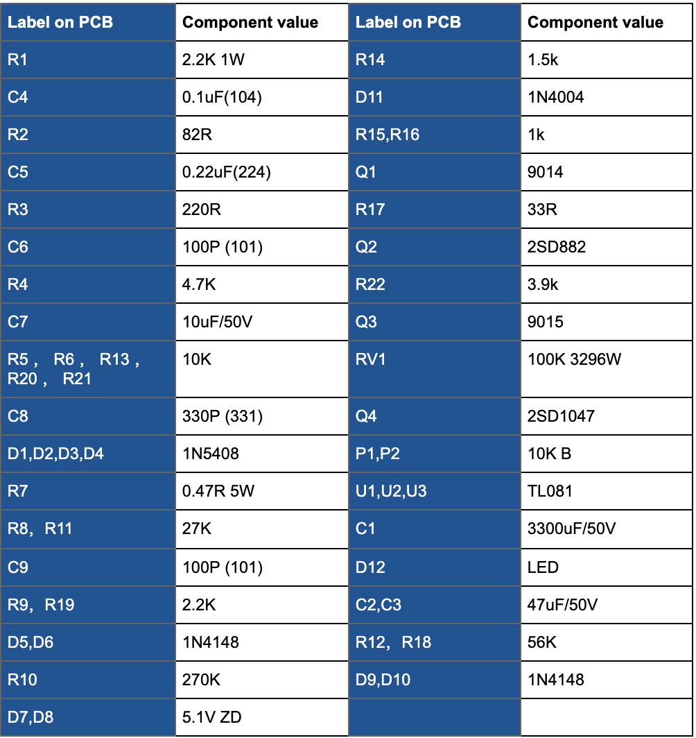
The assembly process for the power supply kit is fairly straight forward. The components in the kit are through-hole type, so all you will need to do is find where each component is meant to be on the board, place it, and solder it. Before soldering, it is important to ensure the orientation of the component is correct, especially for components like diodes and ICs, as placing them wrongly could damage the component itself or the whole board. To make the component placing easy, a table showing the labels on the PCB and the value of the component to be placed is provided below.
If you are not familiar with things like color coding for resistors, it might be helpful to have a meter with you to check the value of the resistors and confirm orientations before soldering. For ICs, you can look up the pinout diagrams/datasheets.
With all the components mounted, the board should look like the image below;
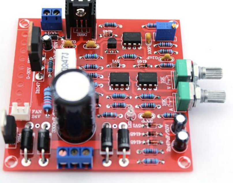
For the voltage and current adjustment potentiometers, you can solder them directly on the PCB as shown above, but to allow more flexibility for your enclosure, you should connect them to the board through socket and jumper wires as shown below.
The potentiometer tagged with A is the current limit potentiometer and V is the voltage potentiometer. In place of the regular potentiometers, for easier and more accurate adjustments, you may replace the voltage potentiometer that came with the kit, with a 10K multi-turn wire-wound potentiometer.
With all the components soldered on the PCB, one last thing we need to do to test the power supply module is to install a cooling fin of considerable size, insulated from the circuit, on Q4 (D1047). A lot of heat will be generated at this end of the circuit and it could lead to a breakdown if it is not properly handled. If the cooling fin is not big enough, you can make use of a cooling fan. The 24V socket on the board was placed there for this purpose. After installing the cooling fin and fan, the board should look like the image below.
Go over the connections once again though to ensure everything is as it should be. With this done, the Power Supply is ready to go. We can now move to the other parts of the project.
Build the Metering Shield
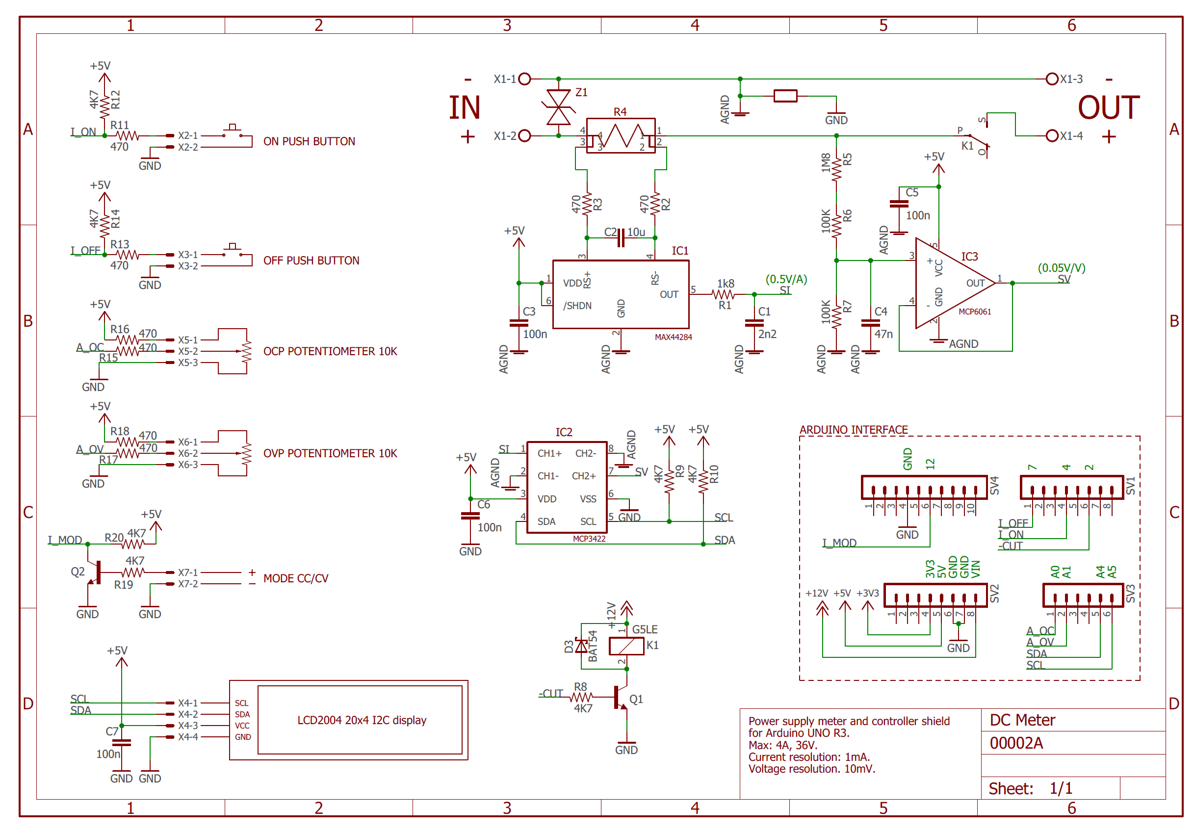
Up next is the metering shield. As mentioned during the introduction, the metering shield helps digitize the controls and provides visual feedback to the user. It also implements the shutdown overvoltage and overcurrent features which disconnects the load via a relay.
As the name implies, the metering circuit was designed as a shield, compatible with all boards that have the layout and dimensions of the R3 version of the Arduino Uno. Due to the shielding nature, it was implemented on a PCB which was designed using Eagle CAD.
The schematics below show how the components are connected:
All design files including, schematics, PCB, and Gerber files are attached under the download section at the bottom of the page. This makes it easy for those who may like to make changes to the design and those who want to just ship the Gerbers off to fabricators and replicate the exact design.
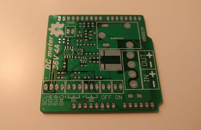
An image of the PCB after production is provided below.
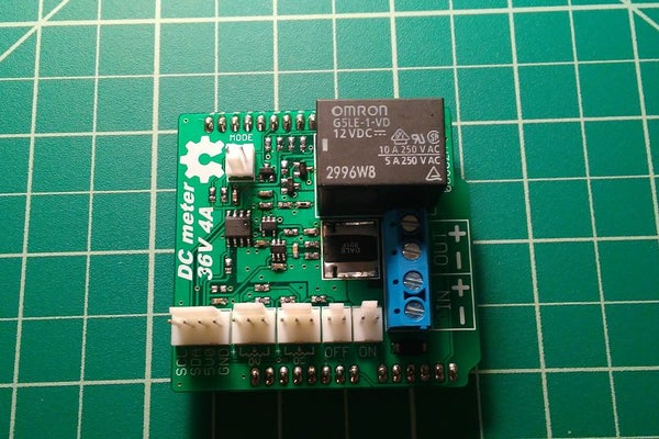
After assembly, the shield should look like the image below;
With the metering shield and the Power Supply all in place, its time to couple them together to create the Lab Power Supply.
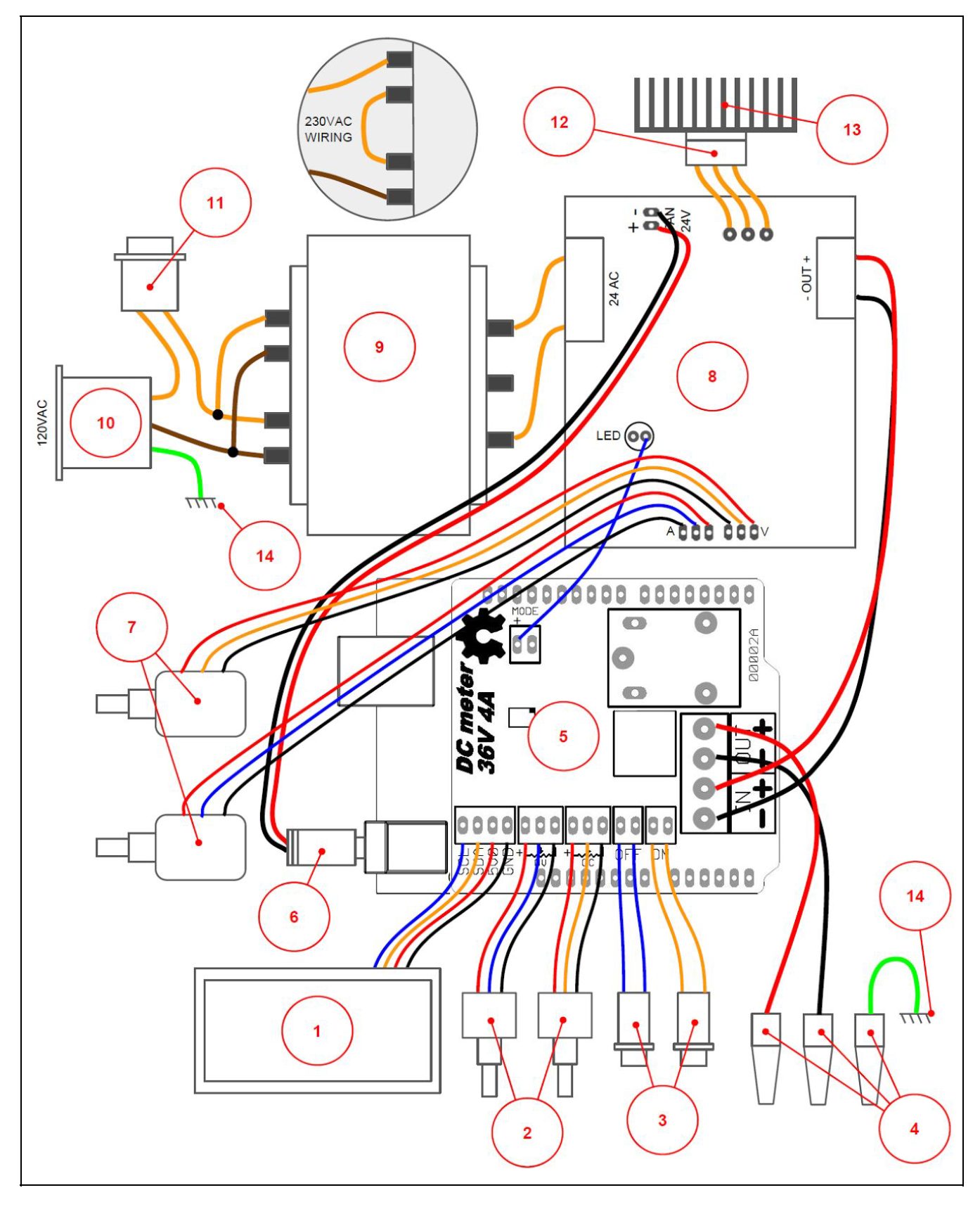
Schematics
Connect the power supply, the metering shield, the Arduino, the display, and other parts of the system together as shown in the schematics below.
The schematics is labeled to make it easy to identify which component goes where. A lookup table for the labels on the schematic is attached under the download section.
AC power source to the system is feed via the transformer which steps the voltage down to 24Vac. It is important to note that the input AC Voltage to the Power Supply Module is 24v and ensure you use a transformer which is rated for such. The system might behave in an unstable manner if a voltage is higher than this. The output of the Vkmaker power supply circuit kit is connected to the IN terminal block of the metering shield and the OUT terminal block of the metering shield goes directly to the binding posts of the Lab power supply. The Arduino is powered over its DC power jack, with supply from the 24V terminal on the power supply.
With all the components connected, we can now proceed to examine the code for the project.
Code
The code for this project was developed using the Arduino IDE. Asides creating a fascinating user interface, the code basically displays the set voltage and current level of the power supply and updates the display as those values are changed by adjusting the potentiometers.
The code is quite bulky but I will try to go over the basic parts, and explain the role of each section.
The code started as usual, with the inclusion of the libraries that will be used. In this case, the I2C version of the liquid crystal library, along with the wire library was used. The wire library implements some of the functions required for I2C communication while the I2C Liquid Crystal library helps with displaying data on the I2C based LCD display. The wire library comes pre-installed with the Arduino IDE and the I2C Liquid Crystal library can be installed via the library manager or manually, via the attached link.
Next, we create some general parameters and variables like the max current and voltage, and output values among others that will be used in the code.
//General parameters
#define MAXVP 2600u           //Maximum OV in 1/100V units
#define MAXCP 3100u           //Maximum OC in 1/1000A units
#define DEBOUNCEHARDNESS 10u

//General variables
uint16_t u16VOValue = 0; //Voltage output value
uint16_t u16COValue = 0; //Current output value
uint16_t u16VPValue = 0; //Voltage protect value
uint16_t u16CPValue = 0; //Current protect value
uint16_t a3u16VP[3u] = {0, 0, 0}; //Array for filtering voltage protect
uint16_t a3u16CP[3u] = {0, 0, 0}; //Array for filtering current protect
uint8_t u8Index_a3u16VP = 0; //Index of a3u16VP
uint8_t u8Index_a3u16CP = 0; //Index of a3u16CP
bool bOnPressed = false;      //State of On push button
bool bLastOnPressed = false;  //Last state of On push button, used for flange detection
bool bOffPressed = false;     //State of Off push button
bool bLastOffPressed = false; //Last state of Off push button, used for flange detection
uint8_t u8OnDebounce = 0;     //Debounce counter for On push button
uint8_t u8OffDebounce = 0;    //Debounce counter for Off push button
bool bMODECV = false;         //Mode of power supply, true: constant voltage, false: constant current
uint32_t u32MCP3422Value = 0;       //Last conversion value from MCP3422
bool bMCP3422ValIsPositive = true;  //Last conversion sign, in this circuit it's always positive
bool bValuesOK = false;             //Indicates in the main loop if the last execution of MCP3422_Machine updated u16VOValue and u16COValue
/////////////////////////////////////////////////////////////////////////////////////
Next, we move to the void setup() function. We start the function by calling the setupDisplay() function which initializes the LCD with the right column and row numbers among other things. We follow this by setting the speed for wire communication so as to set the communication speed for the display and ADC, turn on the LCD backlight, and finally initialize the MCP ADC.
void setup()
{
  RELAY_OFF;
  setupDisplay();
  Wire.setClock(400000);  //Speed for both display and MCP3422
  restartBackLight();
  MCP3422_MachineInit();
}
Next, we write the void loop() function. The void loop function is quite simple thanks to all the functions doing the heavy lifting. The loop() starts with the UpdateInputs() function, which essentially fetches the state of the pushbuttons along with voltage and current value from the ADC.
void loop()
{
  updateInputs();
Next, we call the refreshbacklight() function which is called periodically to ensure the screen’s backlight is on. After this, we verify the state of the ADC and if all is ok, we call the updateStatus() function (which sets the state of the relay), followed by the updateDisplaybuffer() function which modifies the display buffer with current values of the measurements, Finally, we call the updateDisplay() function which browses through the displayBufferA. If any character is different in displayBufferA than displayBufferB writes it to displayBufferB and the LCD.
Other parts of the code are the functions that were called in the setup() and loop() functions and they are properly commented so they should be easy to understand.
The complete code for the project is bulky and might make the post unnecessarily long. To prevent this, the complete code for the project has been attached under the download section.
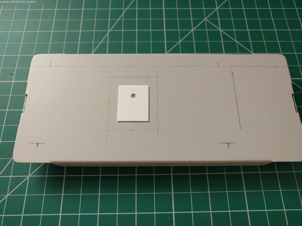
Enclosure
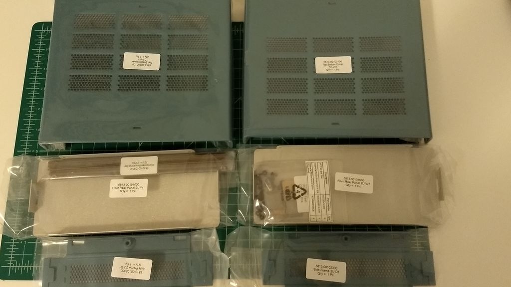
Consistent with Danielrp’s projects, the enclosure for this project is a beauty to behold. It is based on an aluminum enclosure from Cheval (their standalone SA-Series enclosure).
The SA-Series Enclosure
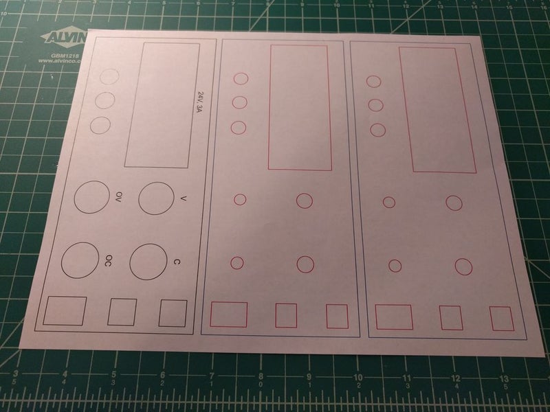
In the absence of a router to modify the enclosure to suit the needs of the power supply, the old way of cutting, trimming with file, and using transfer letters for the text, was adopted. An Inkscape file with the stencil used in cutting the front panel is attached to the zip file under the download section. You can print this and use it to trace out your design on the front panel or cut using a router.
Stencil for Front Panel
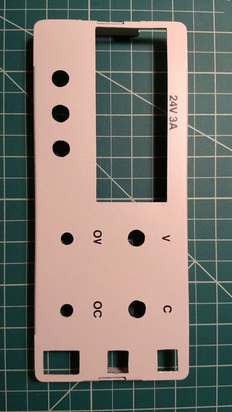
The front panel after cutting and trimming should look like the image below.
Front Panel After Cutting
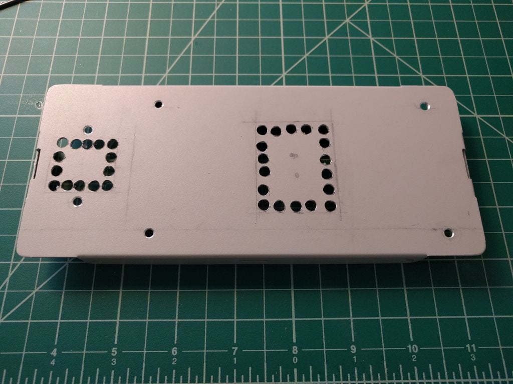
The back panel of the enclosure also requires modification so the heat sink and the IEC Connector for Power could be mounted. To achieve this, follow the steps below;
1. Mark the position of the heatsink, including the hole for the power transistor and the position of the holding screws.
2. Mark the hole for accessing the heatsink from the interior of the power supply enclosure, I have used the insulator as a reference.
3. Mark the hole for the IEC connector.
4. Drill the contour of the shapes.
5. Drill the holes for the screws.
6. Cut the shapes with cutting pliers.
7. Trim the shapes with a file.
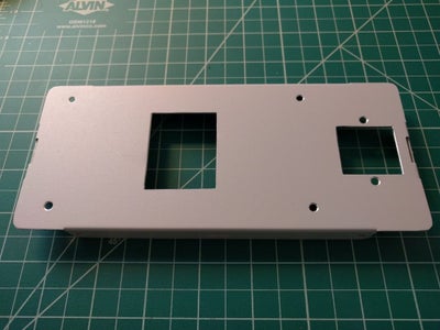
Back Panel after cutting and trimming
It is important to reiterate the importance of the heatsink at this point, as the power supply circuit is not self-protected against overheat. According to the datasheet the 2SD1047 transistor has a junction to case thermal resistance of Rth-j,c = 1.25ºC/W, as such, before buying a heat sink you must take into consideration its thermal resistance and evaluate its suitability based on other factors. A guide to understanding how heat sink calculations work is provided here. but for the sake of this project, this heat sink, with a thermal resistance of Rth-hs, air = 0.61ºC/W, was used and it seemed to be good enough after calculations.
Project Assembly
With the enclosure and electronics in place, it is time to assemble the electronics into the enclosure.
To start with the front panel, follow these steps to position the components;
Strip out a multiconductor cable from scrap to get cables.
Build the “Molex connector”, wire and shrinkable tube assembly for potentiometers, pushbuttons, and LCD. Remove any protuberance in potentiometers.
Remove the pointer ring of knobs.
Cut the rod of potentiometers to the size of the knob. I have used a piece of cardboard as a gauge.
Attach the pushbuttons and power button.
Assemble the potentiometers and install the knobs, the multiturn potentiometers have a ¼ inch shaft and the one turn models have a 6mm shaft. You can use washers as spacers to trim the distance of potentiometers.
Screw the binding posts.
Put a double-sided tape in the LCD and stick it to the panel.
Solder the positive and negative wires to the binding posts.
Assemble the GND terminal lug in the green binding post.
Front Panel After Assembly
With the front panel in place, arrange the back panel with the heat sink following the steps below;
1. While the paint on the enclosure is a good thermal isolator, you can add some heatsink grease to increase the heat transfer from the heatsink to the enclosure.
2. Screw the heatsink to the back panel.
3. Assemble the IEC connector.
4. Position the adhesive spacers using the power supply kit circuit.
5. Screw the power transistor and the insulator, there must be thermal grease in each surface.
6. Assemble the 7812 for powering the Arduino, it should face the case to allow heat dissipation, using one of the screws that hold the heatsink. A plastic washer like this http://www.ebay.com/itm/100PCS-TO-220-Transistor-… could also be used but the project used the same insulator as the power transistor and a bent piece of the case.
7. Finally, Wire the power transistor and the 7812 to the power supply circuit.
Finally, assemble the transformer, DC meter, Arduino + metering shield, and other components, in the enclosure. You can follow these steps to get that done;
Mark and drill the holes for the transformer.
Assemble the transformer.
Stick the adhesive legs of the enclosure.
Stick the DC meter circuit using adhesive spacers.
Scrape the paint to screw the GND lug.
Build the mains voltage wire assemblies, all the terminations are 3/16” Faston. Shrinkable tubes were used to isolate the terminations.
Cut the front part of the holder of the enclosure on the right side to get space for the power pushbutton.
Connect all wires according to the assembly guide provided under the schematics section.
Install the Fuse (1A).
Put the output voltage potentiometer (the VO potentiometer), to the minimum CCW and adjust the output voltage the closest possible to zero volts using the multiturn fine adjusting potentiometer of the vkmaker power supply circuit.
Close up the enclosure.
with this done, the Super Lab Power Supply is now ready for testing and usage.
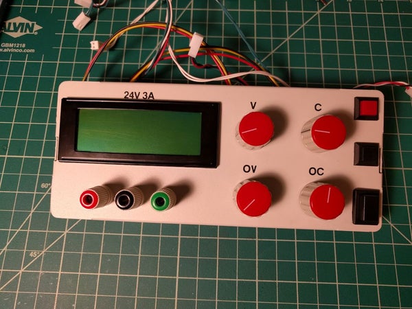
Demo
With all the components assembled and code uploaded to the Arduino, take a minute to admire yourself for a job well done, and plug in the power supply to your AC socket. Push the button and you should see the screen come up as shown in the image below. You should also see the progress bar(along with the voltage/current at the output) change as you turn the knob of the potentiometers.
Go ahead and test the other features and modify them until you are satisfied.
That’s it! Your very own lab power supply!!
Going Forward
So much advancement can be brought into this project thanks to the metering shield. One of the first things that come to mind is being able to control and monitor the power supply via an app over WiFi or Bluetooth by adding an ESP8266 WiFi or a BT/BLE module to the project. Do you have other cool ideas? share via the comment section.
When engineers design electronic circuits, they keep track of many different parameters, but one of the most important is power. In a modern circuit, the power evolves during its many stages, and sometimes it needs to be increased with amplifiers due to much loss caused by dissipative elements.
It is usually preferred to maximize the power transfer between every stage of a circuit in order to avoid as much as possible any reamplification. This is, for example, the case with the transmission of information in the telecommunication domain.
In this tutorial, we focus on a simple but important concept called the Maximum Power Transfer Theorem (MPTT) which explains how power is most efficiently transmitted from a source to a receptor.
To introduce this concept, we will first make a simple observation on a Thevenin circuit in order to understand that the power transmitted depends on the resistor values. We also emphasize the distinction that needs to take place between the optimization of power transferred and the efficiency of the circuit.
In the second section, we explain the MPTT in the general case and prove it by providing a demonstration.
Finally, we focus on the Impedance Matching concept which is linked with this theorem and is an important technique used to optimize the power transfer.
Presentation
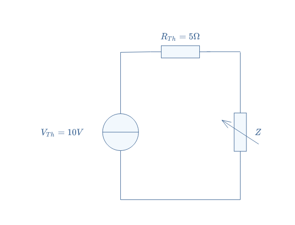
Consider a linear electrical circuit that can be reduced to a given Thevenin equivalent model VTh, RTh which is connected at its terminal to a variable load Z such as illustrated in the following Figure 1:
fig 1: Thevenin model of a circuit supplying a variable load Z
As shown in this Figure, we will consider specific values for VTh and RTh. The common current flowing into the circuit can be written thanks to Ohm’s law: I=VTh/(RTh+Z).
Since the power transmitted to the load can be expressed as PZ=Z×I2, we can develop this expression to write PZ as a function of Z and the known parameters of the circuit: PZ=(Z×VTh2)/(RTh+Z)2.
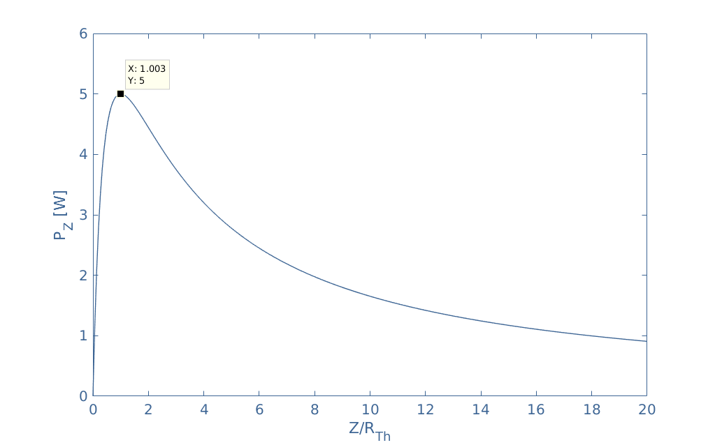
Figure 2 below shows the graph PZ=f(X) where X=Z/RTh, it is plotted thanks to a data software such as MatLab®:
fig 2: Graph PZ=f(Z/RTh)
As highlighted in this Figure, it appears that the maximum power transmitted is reached for Z=RTh. This peak is however not very narrow since the power transmitted is still at 90% of the maximum value for a ratio X=2.
It is important to note that the maximum efficiency defined by the ratio η=PZ/PS, with PS being the power generated by the source, is not reached for X=1 which is exclusively the condition of maximum transferred power. This distinction is confusing and has already been quite detailed in one of our previous articles here: Input and Output Impedances of Amplifiers.
We can note that when the maximum transferred power is achieved, an efficiency of only 50 % is observed. This number can quite easily be explained by the fact that when RTh=Z, the dissipated power by the internal source resistor (RTh) is the same as in the load Z. Maximum efficiencies are reached when the inequality Z>>RTh is satisfied, in this case, no power is dissipated in the internal source resistor.
Maximum Power Transfer Theorem (MPTT)
In this section, we present the general form of the MPTT and furthermore propose a demonstration.
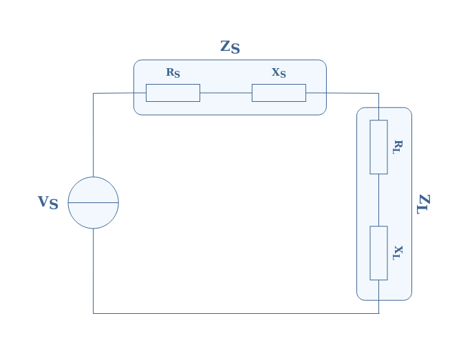
We propose the following Figure 3 as an illustration to refer to:
fig 3: A power source (VS, ZS) supplying a load (ZL)
This circuit can either be considered as a Thevenin model, with VS=VTh and RS=RTh as the equivalent resistance of a circuit between a source and the load, or an unideal source with its internal impedance ZS=RS+jXS supplying a complex load ZL=RL+jXL.
The MPTT states that in order to maximize the power transferred to the load, an impedance matching is required. Two conditions must be satisfied for that:
The reactances must be compensated, that is to say, XS=-XL
The resistances must match, that is to say, RS=RL
Since Re(ZS)=Re(ZL) and Im(ZS)=-Im(ZL), we can say that ZS and ZL are conjugated (see our tutorial about Complex Numbers for more information). Under this condition, the power delivered in the load RL is maximum and satisfies Equation 1:
eq 1: Value of the maximum transferred power
Demonstration
The demonstration of this theorem consists of expressing the power in the load and find its maximum with a derivation operation.
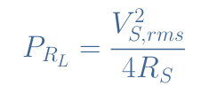
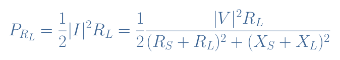
We start by writing the module of the current across the circuit: |I|=|V|/(|ZS|+|ZL|). The power transferred to the load can be expressed with the RMS value of |I|, which square value is IRMS2=|I|2/2.
The power in the load satisfies, therefore:
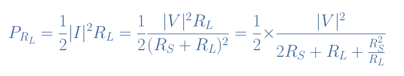
In order to maximize this fraction, we will minimize the denominator. The term of the reactances can be easily minimized and even compensated by choosing XS=-XL.
The expression of power can then be simplified:
In order to minimize again the denominator D, we proceed to a derivation which is equalized to zero: dD/dRL=0. This derivation leads to -RS2/RL2+1=0⇒RS=RL.
However, when the derivative is equal to 0, either a maximum or minimum can be reached. In order to make sure that RS=RL is a minimum, we compute the second-order derivative d2D/dRL2=2(RS2/RL3).
For positive values of RS and RL, the second-order derivative is positive, which means that the denominator is a convex function (the same shape as the function x2). We can then confirm that a minimum is reached for RS=RL.
As a conclusion, the power in the load is maximum when RS=RL and XS=-XL. When these conditions are met, we can confirm that Equation 1 is satisfied.
Impedance Matching
We have briefly mentioned the term impedance matching in the previous section, here we explain how important this concept is, especially in the telecommunication domain.
The impedance matching technique is used to optimize the power transfer and not the efficiency.
The impedance matching technique is very used to optimize the signal transfer in transmission lines. A transmission line is a special double-wire that is adapted to conduct high-frequency signals with minimal losses.
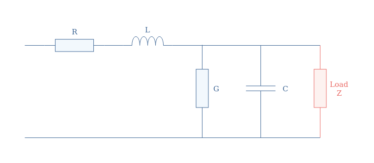
They are usually represented by an equivalent circuit represented in the following Figure 4:
fig 4: Representation of a transmission line connected to a load
We need to note that the components shown in Figure 4 are not truly present in a transmission line, this representation exists in order to reflect the electrical behavior of the line.
The linear resistance and inductance of the line are represented by R and L. The properties of the material in between the two conductors are represented by the conductance G and the capacitor C. The load Z connected at the terminals of the transmission line can represent a television, an amplifier, a phone… etc
We define the characteristic impedance by ZC=√(L/C) which represents the impedance of the transmission line. Analogically with Ohm’s law, this particular impedance simply represents the ratio of the voltage and current propagating in the transmission line. A coaxial cable, for example, is a transmission line with ZC=50 Ω.
The expression of the characteristic impedance comes from the famous telegrapher’s equations, which itself, comes from the Maxwell’s equations of electromagnetism.
Ensuring that the power is optimally transferred from the source to the load is very important in this example. Matching the load Z with the characteristic impedance of the line indeed avoids reflections of the signal back towards the source, which would cause interference. In a phone line, for example, a poor impedance matching can be heard with echos.
Conclusion
For some circuits, a maximum of the power transferred is desired, especially in the telecommunication domain. We present in this article the Maximum Power Transfer Theorem (MPTT) which explains under what requirements this condition is met.
In the first section, we observe from a Thevenin circuit that the maximum power transferred is reached when both the resistor present in the circuit are equal. We also explain that it is important not to mistaken the maximum power transferred with the efficiency of the circuit, despite the similarities in their definitions.
In the second section, we detail the MPTT by explaining that two conditions are required in order to achieve the maximum power transferred. Not only the resistor must be equal but the reactances must compensate each other. Furthermore, a demonstration of the theorem is provided, which can help the reader to understand the difference between this theorem and the efficiency concept.
Finally, a small section details the concept of impedance matching in the telecommunication domain.
Altium 365 platform empowers designers to work from anywhere, and connect with anyone.
Altium, LLC, a leader in PCB design software, today announced the availability of Altium 365, the world’s first cloud platform for PCB design and realization. The platform is poised to transform the electronics industry by bridging the gap between PCB designers, part suppliers, and manufacturers through seamless collaboration as the design evolves.
Altium 365 works harmoniously with Altium Designer, the industry standard for PCB design, to deliver the most connected experience for PCB design and manufacturing. This allows design teams to drastically reduce miscommunication, re-design iterations, and time to market.
“A long-term change in the way that the various stakeholders in the electronics industry work together is taking place,” said Ted Pawela, Chief Operating Officer at Altium. “Whether working from home, office or traveling for business, the need to work from anywhere in the world without being tethered to your desktop is here to stay. Altium is paving the way for engineers and designers to work from anywhere, and connect with anyone by making the Altium Designer user experience more collaborative and more readily available than ever before.”
With Altium 365, users can bring together the stakeholders and participants of their choosing (even those who do not have Altium Designer), while keeping their IPs secure and design under control. This cloud-based platform provides a completely new way to share, visualize, and mark-up PCB designs for all stakeholders involved, from design managers to manufacturers, while allowing other designers to connect to the same PCB design with Altium Designer to author changes.
Teams can organize designs, libraries, and participants in one place, and share links to their designs for easy, real-time collaboration. Designs are always accessible at any time, on any device, anywhere. By leveraging CAD-specific intelligence, design data can be stored in a way that makes projects, files and version history accessible and easy to navigate on the web.
“We use the Altium 365 workspaces as a way to keep all our components, designs and projects all in one place, so that everyone is working from the same source of information. We are able to design faster with teams at different locations.” – Chris Brawn | Senior Design Engineer | Skyships
Altium 365 provides a built-in co-designer capability between electronic and mechanical domains through native integration with PTC Creo®, Dassault Systèmes® SolidWorks™ and Autodesk Inventor®. PCB designers and mechanical CAD designers are now able to collaborate more efficiently and creatively than ever before.
Altium 365 also helps streamline the manufacturing process. Designs can be packaged and shared with internal and external shareholders with just a simple web link that can be accessed via any platform on any internet-enabled device.
“We are using Altium 365 in our manufacturing process. We can immediately share the Bill of Materials and version updates, so our manufacturers can know if something changed and why right away.” – Dario Pennisi | Hardware Development Manager | Arduino
By adding the flexibility of sharing and collaboration of the cloud to the power of desktop PCB design software, Altium is making a big leap towards unifying the electronics industry.
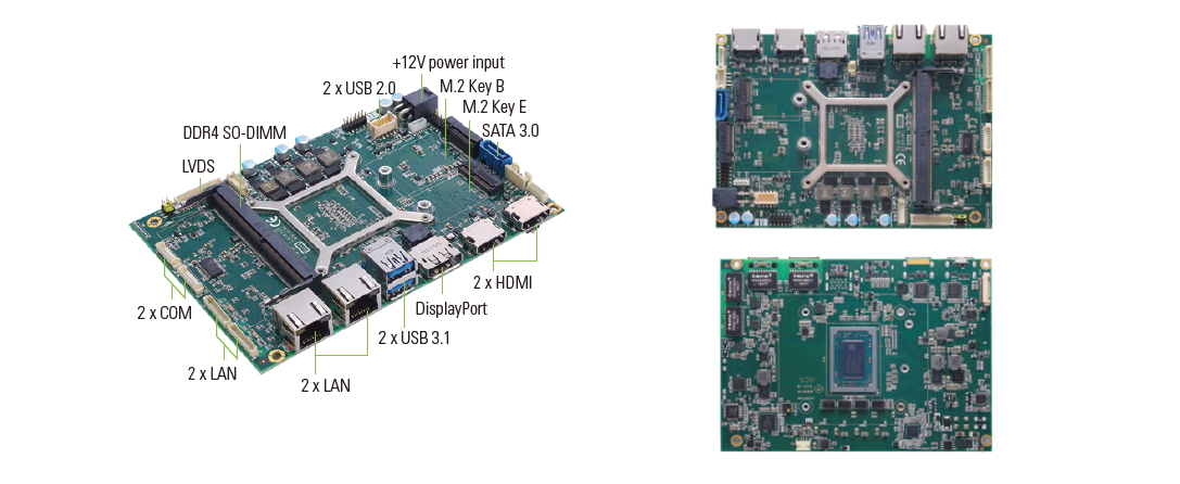
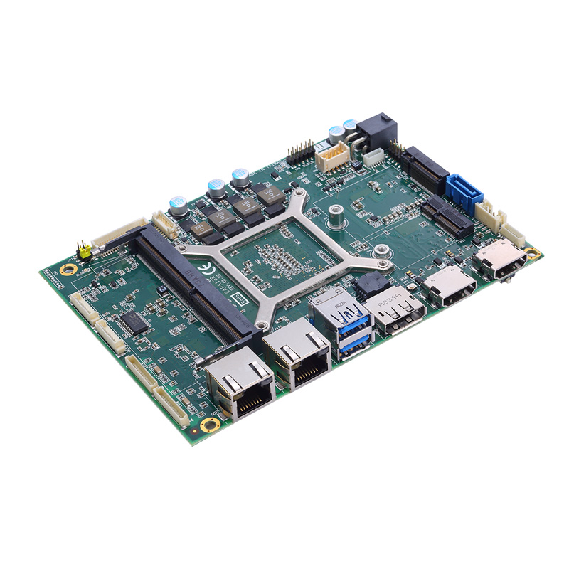
Axiomtek – a world-renowned leader relentlessly devoted in the research, development and manufacture of series of innovative and reliable industrial computer products of high efficiency – is pleased to introduce the CAPA13R, a high-performance 3.5” embedded board with quad displays. The CAPA13R is powered by the onboard AMD RYZEN™ Embedded V1807B/V1605B processor with AMD Radeon™ RX Vega graphics. The embedded board is well-suited for graphics-intensive applications such as medical imaging, video surveillance, 3D simulators, optical quality control, digital signage, kiosks/POI, thin clients, and more.
The integrated AMD Radeon™ RX Vega graphics with support of DirectX 12 and OpenGL 4.5 marks the cutting edge of embedded graphics. The CAPA13R offers quad display capability through two HDMI, one DisplayPort and one LVDS interfaces. Its onboard CPU is attached on the rear side of the board, which can aid with heat dissipation and offers flexibility for easy system integration and minimum maintenance. Moreover, the CAPA13R offers multiple expansion interfaces with one M.2 Key E slot for wireless modules and one M.2 key B slot for storage cards. One 260-pin SO-DIMM socket on the CAPA13R supports up to 16GB of DDR4-2400 (V1605B) and DDR4-3200 (V1807B) memory. The system has a +12V DC power input.
“The new AMD RYZEN™ Embedded V1000 series is the best choice for embedded solutions that require a high-resolution display and full-graphics feature, and offers the benefits of a smaller footprint,” said Michelle Mi, Product Manager of Embedded Board and Technology Business Unit at Axiomtek. “The CAPA13R has four GbE LAN ports to connect with industrial cameras for machine vision applications and four independent displays for graphics-oriented appreciations, like digital signage, gaming, infotainment, etc. Its scalability, optimized graphics and low profile design offers a high level of versatility to help system integrators drive their projects forward.”
To satisfy increasing demands of connecting more peripheral devices, the CAPA13R provides two USB 3.1 Gen2, two USB 2.0, four GbE LAN, one RS-232, one RS-232/422/485, two HDMI, one DisplayPort, one LVDS, one SATA-600, 8-channel DIO, one HD audio, and an SMBus compatible with I2C. Furthermore, it supports hardware monitoring features to monitor temperature, voltage, fan speed and more. The built-in watchdog timer keeps the system running smoothly. Additionally, the CAPA13R supports Windows® 10.
Advanced Features:
AMD® RYZEN™ Embedded V1807B and V1605B processors
One DDR4 SO-DIMM for up to 16GB of memory
Four GbE LAN
Two HDMI, one DisplayPort and one LVDS
M.2 Key E (PCIe x1, USB 2.0)
M.2 Key B (SATA default, PCIe x2 for option, USB 2.0)
Axiomtek’s new CAPA13R is now available for purchase. For more product information or pricing, please visit our global website at www.axiomtek.com or contact one of our sales representatives at info@axiomtek.com.tw.
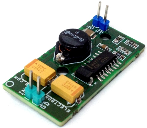
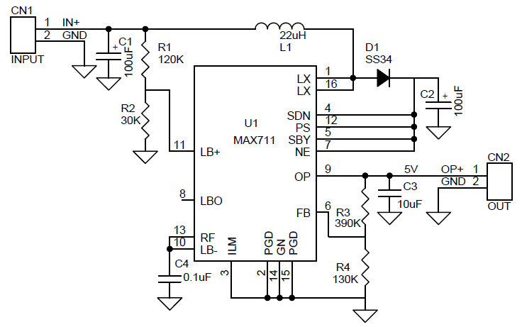
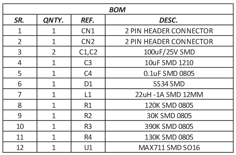
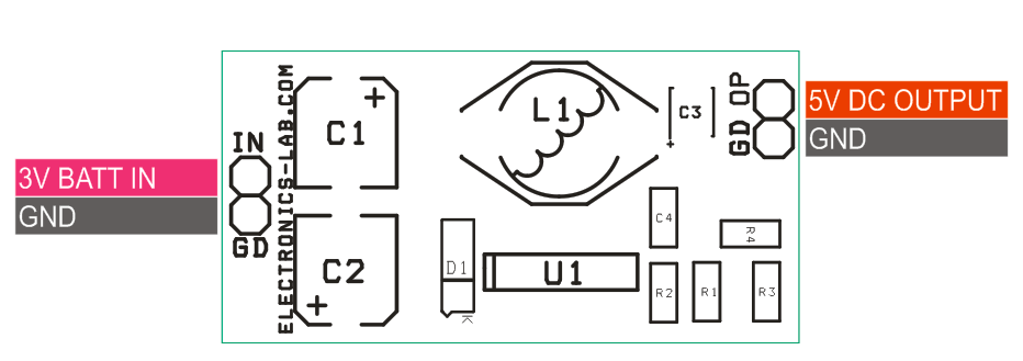
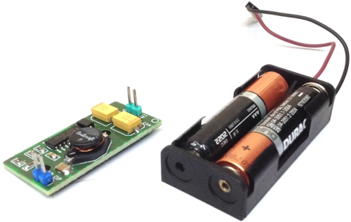
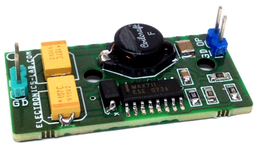
The circuit shown here is a compact and high-efficiency boost converter that has been designed for hand-held equipment. This boost converter converts 2 cells (3V) DC power into 5V DC with output load current up to 500mA. Typical efficiency when boosting battery inputs is 85%. The circuit is based on MAX711 which integrates a step-up DC-DC converter with a linear regulator to provide step-up voltage conversion. The circuit is optimized for battery applications where the input varies above and below the regulated output voltage. The project has an input range from +1.8V to +11V. The circuit is set for 5V output but it has an adjustable output that can be set from +2.7V to +5.5V with the help of two R3, R4 resistors. The IC contains a comparator for low battery detection. If the voltage at LBI+ falls below that at LBI- (typically connected to REF), LBO goes low. Hysteresis is typically 50mV. You can set the low-battery monitor’s threshold with two resistors, R1 and R2.
The MAX711 integrate a step-up DC-DC converter with a linear regulator to provide step-up/down voltage conversion. The step-up switch-mode regulator contains an N-channel power MOSFET switch. It also shares a precision voltage reference with a linear regulator that contains a P-channel MOSFET pass element. Step-Up Operation A pulse-frequency-modulation (PFM) control scheme with a constant 1μs off-time and variable on-time controls the N-channel MOSFET switch. The N-channel switch turns off when the part reaches the peak current limit or the 4μs maximum on-time. The ripple frequency is a function of load current and input voltage.
Features
Supply Input Two AA Cell- 3V DC (+1.8V to +11V Range)