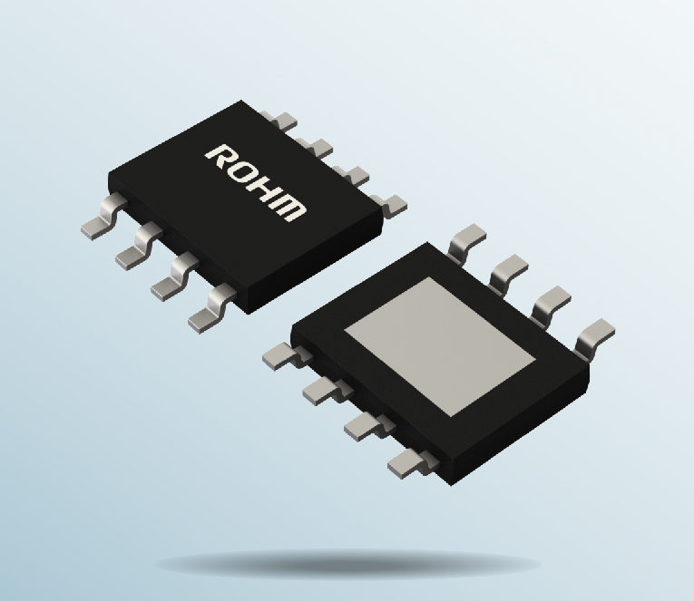
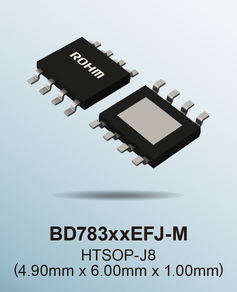
ROHM recently announced the AEC-Q100 qualified 2.8W output Class AB monaural speaker amplifiers the BD783xxEFJ-M series (BD78306EFJ-M, BD78310EFJ-M and BD78326EFJ-M) ideal for instrument clusters – used in vehicles equipped with autonomous driving and ADAS.
In recent years, technological innovations in the automotive field – such as autonomous driving and ADAS – require a greater variety of sounds, such as warning sound when departuring from the lane or for surrounding obstacles. As a result, even audio output systems in the instrument cluster are utilizing speaker amps to generate sound with an MCU, instead of relays that produce blinker sounds and electronic buzzers that emit warning sounds. However, until now it was difficult to ensure safe, stable sound output at loud volumes.
ROHM developed the BD783xxEFJ-M series for vehicle clusters – requiring various sound outputs at high volume, including warning sounds, turn signals, welcome tones and voice guidance. Also, adopting a new type of over current protection (OCP) circuit provides protection against output shorts (damage due to accidental terminal contact) to deliver high 2.8W output that was difficult to achieve in the past, making it possible to deliver high 2.8W output. In addition to over current protection, built-in thermal shutdown and under voltage lock out (UVLO) ensures high reliability protection against abnormal conditions.
Furthermore, satisfying the automotive reliability standard AEC-Q100 and having the capability of withstanding high temperature operation up to 105°C, enable stable voice output without compromising functionality even under severe conditions.
In this tutorial, we present a powerful method that can simplify through some transformation steps, complex circuits into elementary circuits and this method is commonly known as Thevenin’s theorem.
Originally, it was the German physicist Hermann von Helmholtz who first demonstrated the theorem in 1853, but history kept the name of the French engineer Leon Thevenin, who in 1883, unawarely of the work of Helmholtz, proposed a more elegant method to prove the theorem.
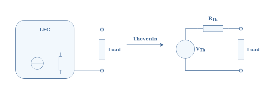
Thevenin’s theorem affirms that any linear electrical circuit is equivalent to an ideal voltage source in series with an equivalent resistor.
We will illustrate this statement in the first section where we also define the bold terms of the theorem. In the second section, we present the method to follow in detail, in order to apply Thevenin’s theorem to a circuit.
Finally, some Thevenin transformations are fully depicted in the last section with real circuits taken as examples.
Presentation and definitions
As previously mentioned, Thevenin’s theorem can only be applied to linear electrical circuits (LEC). The internal structure of LEC consist of interconnected ideal sources and resistors. Reactive components such as capacitors and inductors must be excluded since their voltage/current characteristics are not described by a linear formula.
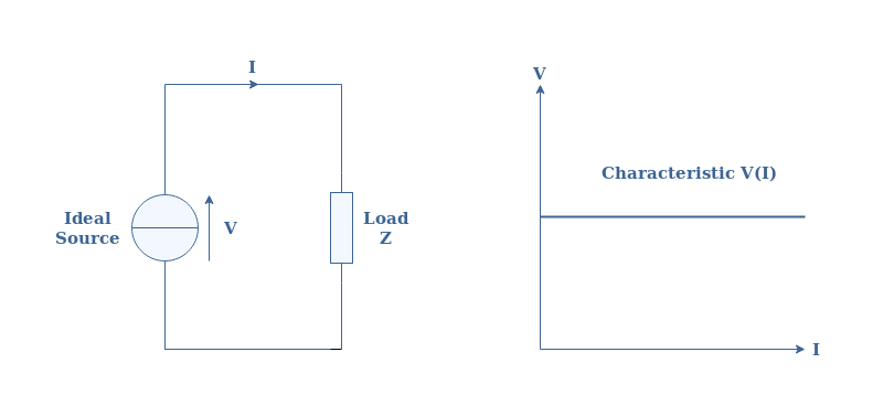
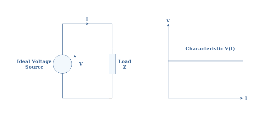
An ideal voltage source consists of a generator that delivers a constant value of voltage regardless of the current flowing in the circuit. This means that the same ideal source will always deliver the same voltage Vs for any circuit connected at its terminals. This property ensures that the voltage/current characteristic of an ideal voltage source is constant and therefore is linear.
fig 1: Representation of an ideal voltage source along with its voltage/current characteristic
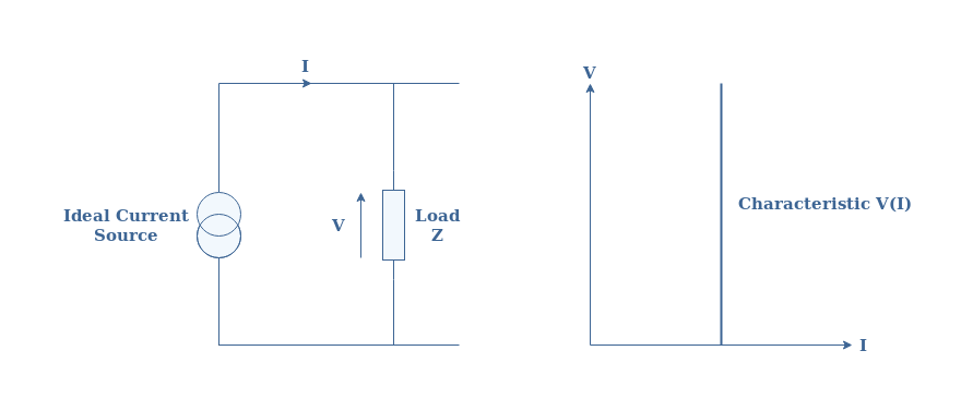
Ideal current sources can also be found in LEC and consist of generators that provide a constant value of current regardless of the voltage at their terminals. A representation of an ideal current source along with its and voltage/current characteristic is proposed in Figure 2 below:
fig 2: Representation of an ideal current source along with its voltage/current characteristic
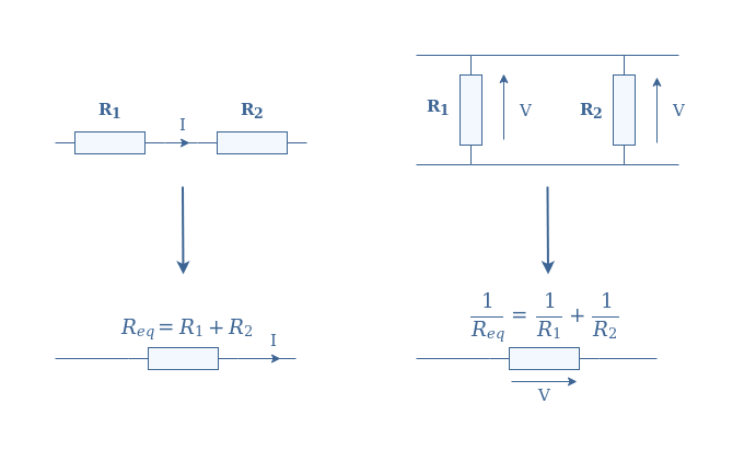
An equivalent resistor Req is simply a concept that represents the association of a set of interconnected resistors (R1, R2,…) into a single component. The association of resistors is dictated by two rules:
If the resistors share the same current (in series), the equivalent resistance is the sum of the resistors.
If the resistors share the same voltage (in parallel), the inverse of the equivalent resistance is the sum of the inverses of the resistors.
fig 3: Rules of equivalent resistance associations
Now that these various definitions have been detailed, we can illustrate Thevenin’s theorem with the following Figure 4:
fig 4: Illustration of Thevenin’s transformation
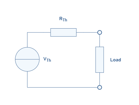
The simpler circuit obtained from the Thevenin transformation is known as the Thevenin model. The equivalent source and resistance are labeled with the subscript Th as a reference to the name of the theorem.
In the next section, we give the abstract method in order to determine this model from any LEC.
Thevenin model determination
The goal of this section is to present how the Thevenin parameters VTh and RTh are determined.
Thevenin’s voltage VTh is the voltage between the terminals of the LEC when the load is disconnected and it is also known as the open-circuit voltage.
Similarly, Thevenin’s resistance RTh is the resistance at the terminals of the circuit when the load is disconnected and all the circuit’s sources are disabled, the voltage sources are replaced with short-circuits and the current sources with open-circuits.
We propose therefore a series of steps to follow in order to determine the Thevenin model of any LEC:
Remove the load at the terminals of the LEC
Compute the voltage of the open-circuit
Replace any voltage sources with short-circuits and the current-sources with open-circuits
Compute the equivalent resistance
Reconnect the load and draw the Thevenin model thanks to the knowledge of VTh and RTh
In the following section, we illustrate this method by determining the Thevenin model of some LEC examples with increased architecture complexity.
Thevenin’s model of some LEC
Single voltage source
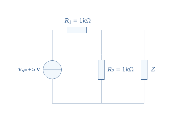
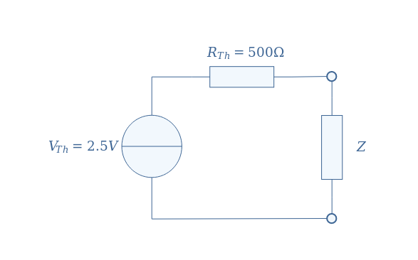
For the first example, we consider a basic LEC composed of only one voltage source and two resistors in a parallel configuration:
fig 5: Single voltage source LEC
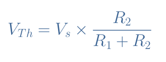
In order to determine Thevenin’s model, first of all, we proceed to steps number 1 and 2 explained in the previous section. When disconnecting the load Z from the circuit, we compute the voltage at the terminals of the LEC, that is to say across the resistor R2, by applying the voltage divider method:
After replacing the parameters by their values, we obtain VTh=2.5 V.
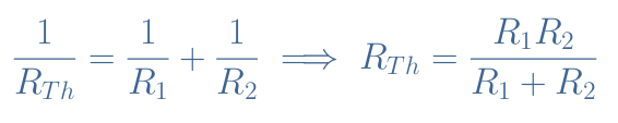
We consider now the circuit by replacing the voltage source by a wire. The equivalent Thevenin resistance is the parallel association of the resistors R1 and R2:
The numerical application gives RTh=500 Ω.
The circuit presented in Figure 5 can, therefore, be simplified by the equivalent Thevenin’s model presented in Figure 6:
fig 6: Thevenin’s model of the single voltage source LEC
The voltage and current across any load Z are now much easier and faster to compute. As an example, if Z=100 Ω, we can use again the voltage divider formula to find VZ=0.4 V. The current is obtained by applying Ohm’s law to the resistance Z: I=VZ/Z=4 mA.
Single current source
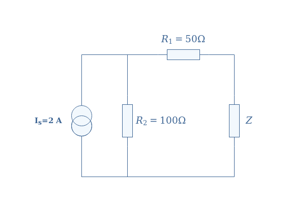
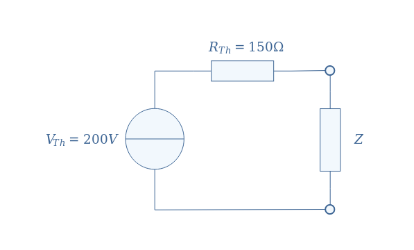
For the second example, we consider a similar circuit than in Figure 5, but replacing the voltage source by an ideal current source and rearranging the resistors:
fig 7: Single current source LEC
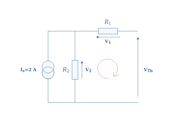
First of all, we disconnect the load Z from the circuit in order to determine VTh:
When applying Kirchoff’s Voltage Law in the loop highlighted with the red symbol, we find VTh=V2-V1. However, since the circuit is opened, no current is observed across R1 and therefore VTh=V2. The current flowing in R2 is thus equal to the current source, we finally apply Ohm’s law to R2 in order to find VTh=100×2=200 V.
Thevenin’s resistance RTh is found by replacing the current source by an open circuit, the equivalent resistor is determined by the series association of R1 and R2: RTh=R1+R2=150 Ω.
Figure 8 below illustrates the Thevenin model of the circuit presented in Figure 7:
fig 8: Thevenin’s model of the single current source LEC
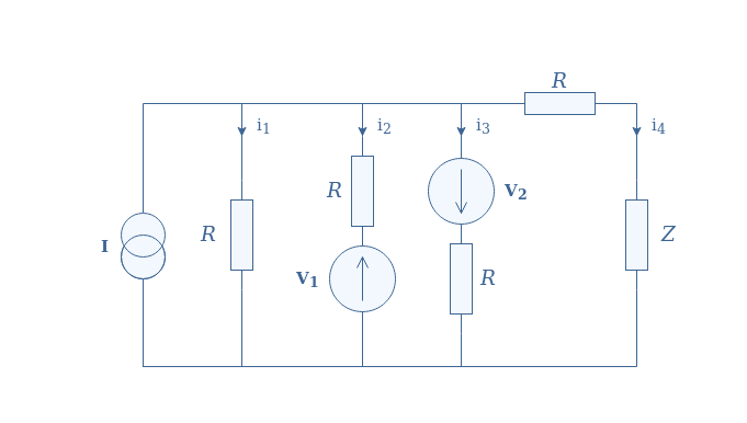
Multi-current/voltage sources
For this last example, we propose a more complex circuit that includes both current and voltage sources:
fig 9: Multi-source LEC
We disconnect the load in order to determine the voltage VTh. It comes automatically that i4=0 since the circuit becomes open. Kirchoff’s current law affirms that I=i1+i2+i3, moreover, we can assert thanks to Kirchoff’s voltage law that:
i1=i2+V1/R
i1=i3-V2/R
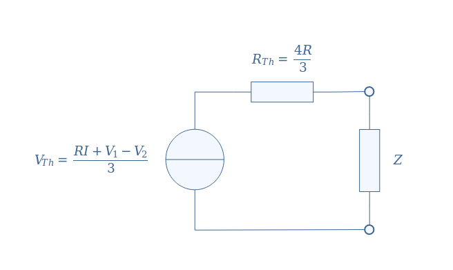
After rearranging these three equations, we can isolate i1=(I+V1/R-V2/R)/3. Thevenin’s voltage is simply given by R×i1, therefore, VTh=(RI+V1-V2)/3.
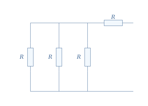
We replace the current source by an open circuit and shorten the voltage sources in order to determine RTh:
The equivalent resistance is given by the parallel association of 3 resistors in series with R, which leads to RTh=R+R/3=4R/3.
Thevenin’s model of Figure 9 is finally given by:
fig 10: Thevenin’s model of the multi-source LEC
Conclusion
“Any linear electrical circuit is equivalent to an ideal voltage source in series with an equivalent resistor.” This sentence, known as Thevenin’s theorem, was the focus of this article.
In the first section, we define the bold terms which give the framework where the theorem can be applied. A linear electrical circuit (LEC) is an interconnection of ideal sources and resistors. Ideal sources are further defined as sources with a perfectly flat voltage/current characteristic. An equivalent resistor is simply a concept that allows us to regroup a set of interconnected resistors into a single component.
In a short second section, we abstractly present how to determine the Thevenin model of any LEC by following a series of steps.
The third section illustrates, with real examples, how to transform a LEC into its equivalent Thevenin’s model. First, we clarify how to proceed for circuits containing either voltage or current sources. Finally, we demonstrate how to perform the transformation with a more complex LEC containing both sources and more resistors.
It becomes especially clear with the last example that Thevenin’s model is a powerful tool to transform complex linear circuits into elementary circuits containing only one source and a resistor.
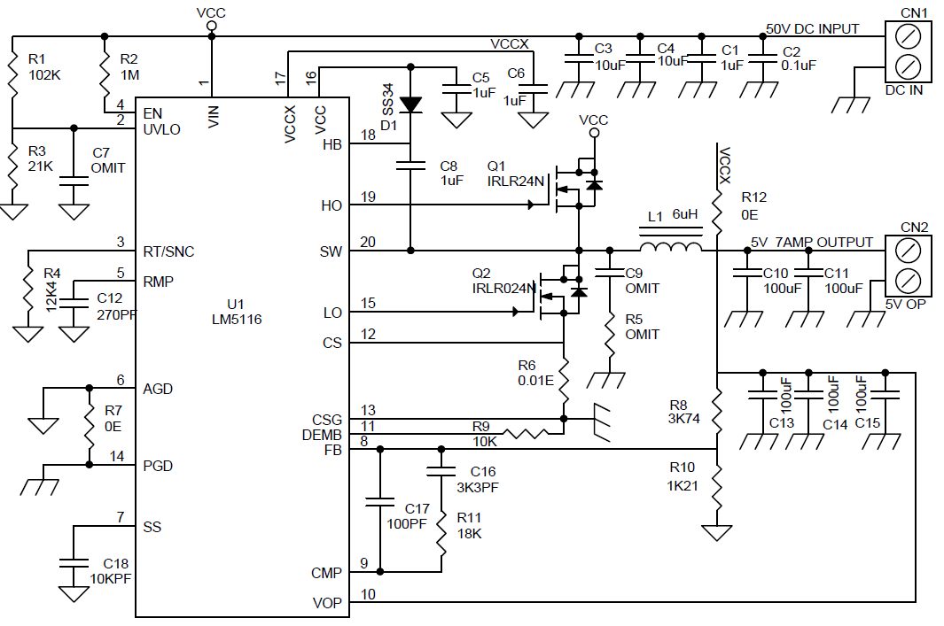
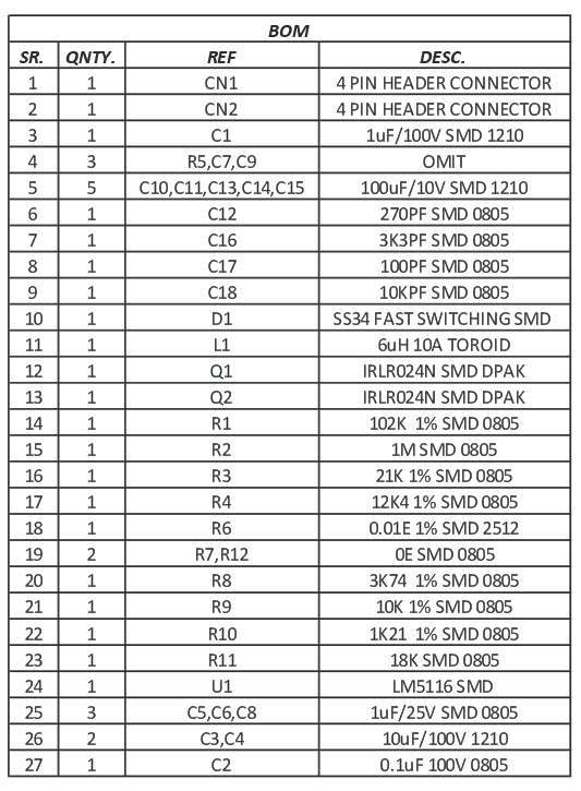
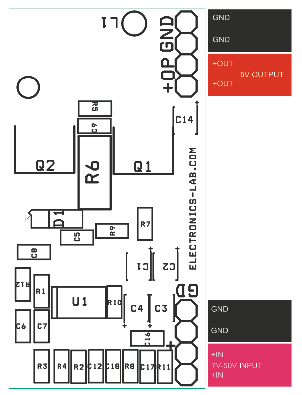
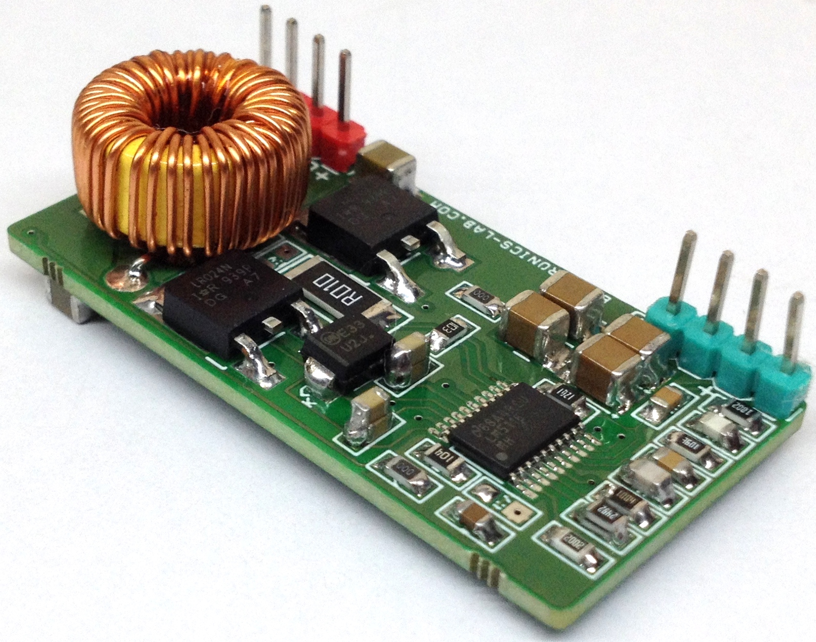
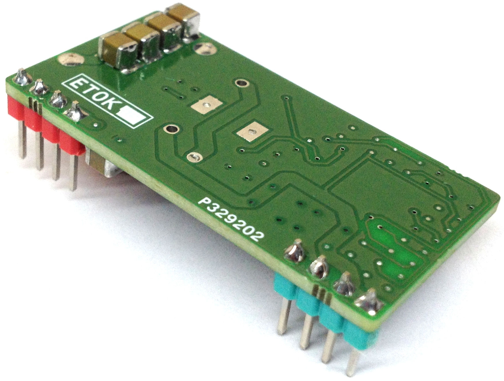
This module is a non-isolated 7A DC-DC converter. The module can convert any DC voltage between 7V to 50V to a 5V DC with load current up to 7A. The project has been designed around LM5116 Wide Range Synchronous Buck Controller IC. The design includes 6uH toroid inductor and two N channel MOSFETS. The operating frequency is 250 KHz.
The LM5116 is a synchronous buck controller intended for step-down regulator applications from a high-voltage or widely varying input supply. The control method is based upon current mode control utilizing an emulated current ramp. Current mode control provides inherent line feed-forward, cycle-by-cycle current limiting, and ease-of-loop compensation. The use of an emulated control ramp reduces noise sensitivity of the pulse-width modulation circuit, allowing reliable control of very small duty cycles necessary in high input voltage applications.
50V to 5V @7A Synchronous Buck (Step-down) Converter – [Link]
CircuitPython is a branch of MicroPhython designed to simplify education and experimentation on low-cost microcontrollers to make it easy to prototype without any upfront desktop software downloads. With CircuitPython, you can write clean and simple Python code to control your hardware instead of using complex low-level languages like C or C ++.
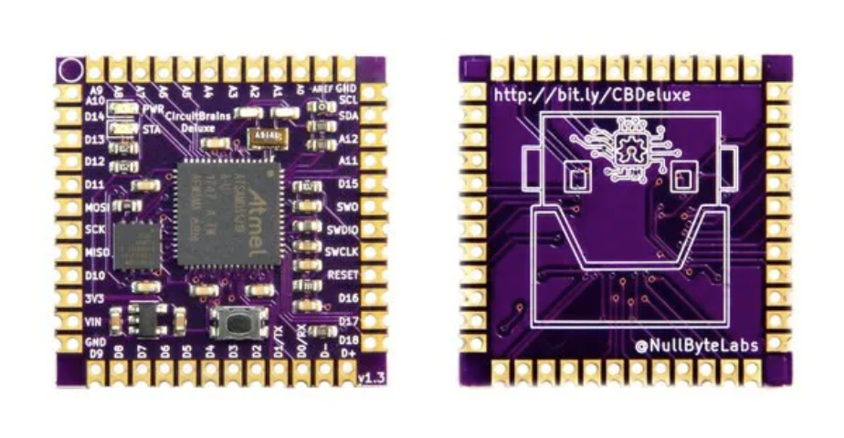
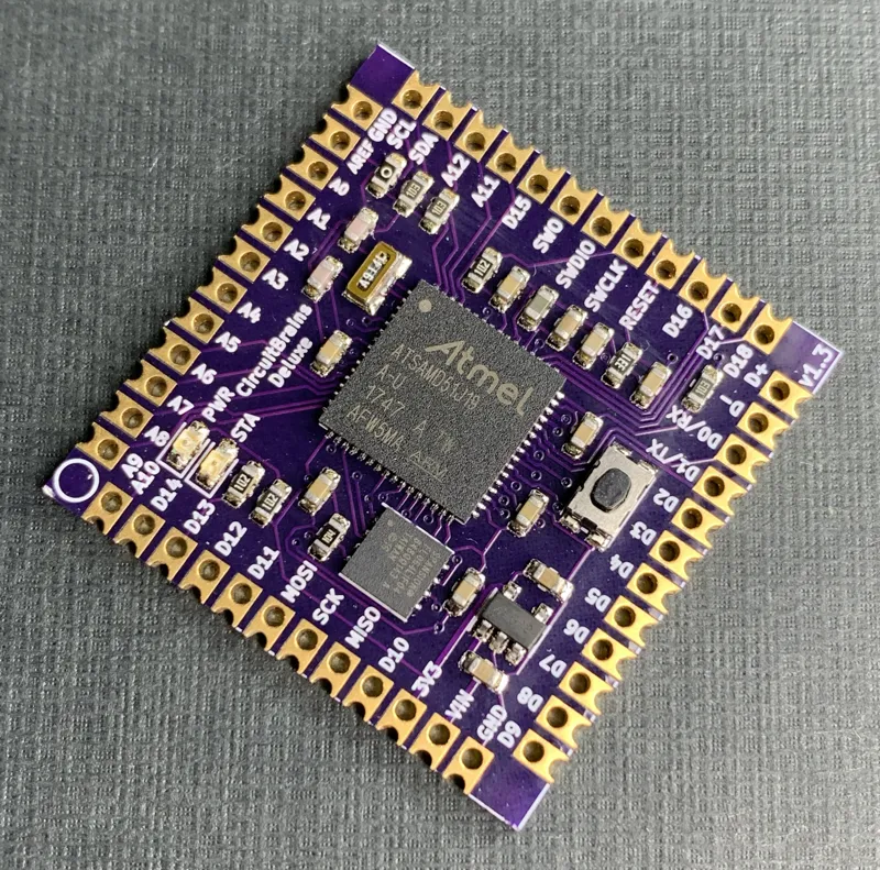
While we have seen several boards developed with Adafruits’ CircuitPython support, the new CircuitBrains Deluxe powered by Microchip SAMD51 seems to be one with a little difference. The CircuitBrains Deluxe, a tiny CircuitPython – compatible ARM Cortex – M4 Module is a 48-pin castellated pad module designed for easy implementation of CircuitPython in maker projects or smooth integration into space-constrained products without the bulk of a large breakout board. Preloaded with a fork of MicroPython, the CircuitBrains Deluxe has other advantages besides being smaller in size when compared with larger CircuitPython compatible boards like Adafruit Metro M4, Adafruit Feather M4 Express or the Sparkfun Thing Plus. The board exposes more I / O pins and has more SPI flash storage memory against the usual 2MB to 4 MB of other boards.
Features and specifications of the board include:
Board Dimensions: 29 x 29 x 3.5 mm (1.15 x 1.15 x 0.15 inches)
32-bit ARM Cortex M4 microcontroller – Atmel ATSAMD51J19 – at 120 MHz, 512KB Flash and 192KB SRAM
8 MB SPI Flash storage capacity
Pin Breakout for SPI, UART, and I2C
Debug / SWD programming interface
Pin Breakouts for Inputs / Outputs – 19 Digital and 13 Analog
LEDs for Power and Status
5v supply voltage power supply
Onboard 3.3 V LDO regulator connected to 3V3 pin
Apparently, since rolling your own microcontroller board can be time-consuming, using CircuitBrains Deluxe in your projects should help save some time and frustration. With CircuitPython support, the CircuitBrains Deluxe when connected over USB opens up the serial console and storage to allow you to modify the codes and see the results immediately after the changes are saved.
Meanwhile, Github has more details about the board including its KiCAD hard design files.
The project was recently launched on Crowd Supply with a $4,800 funding goal. The board is expected to start shipping out in a few month’s time, hopefully after the first half of this year with free shipping to the United States and a $10 cost, to other parts of the world.
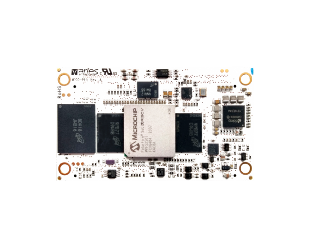
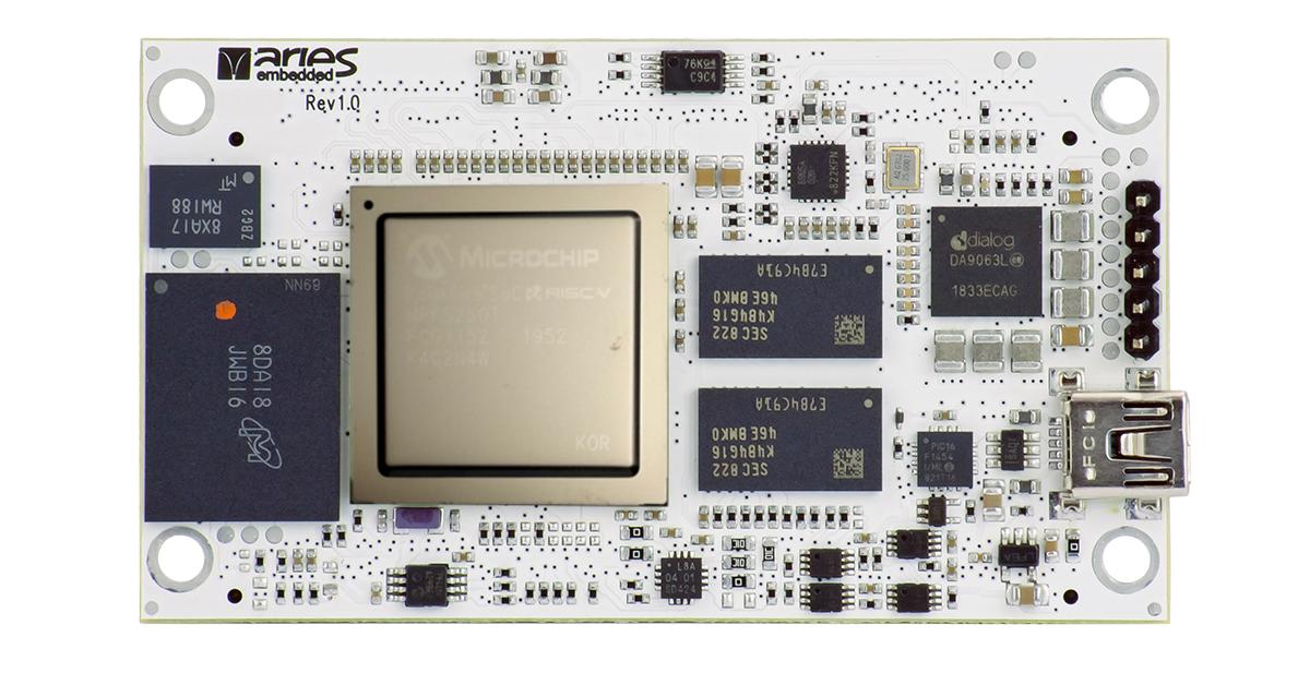
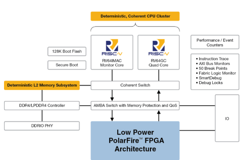
Aries Embedded has launched a Linux-powered, FPGA-enabled RISC-V SoC from Microchip’s Micro semi unit, called the M100PFS. It is one of the first compute modules equipped with the PolarFire SoC. The M100PFS features an identical 74 x 42mm footprint as Aries’ similar M100PF module, which is equipped with the PolarFire FPGA without the Linux-ready RISC-V cores. The M100PFS enables applications like wireline access networks, cellular infrastructure, defense, commercial aviation, industrial automation, and IoT.
The new M100PFS offers support for more entry-level FPGA models, two more versions of the M100PFS module with different FPGA capabilities are available for order with shipments due in Q3 2020. The mid-range 93KLE and 161KLE FPGAs are available only on request. The largest 460K LE capability will be available in a later model. There are two major M100PFS SKUs, namely the M100PFS-025ADA0 — MPFS025T FPGA with 23K LE, 68 math blocks, 4x SERDES, 1GB LPDDR4 RAM for HMS (RISC-V/Linux), 4GB eMMC, and the M100PFS-250AECC — MPFS250T FPGA with 254K LE, 784 blocks, 16x SERDES; 4GB LPDDR4 each for HMS and FPGA; 8GB eMMC. All the models that are available now enable 12.5Gbps SERDES and 2x PCIe root port/endpoints. Available also are 2x 64-bit AXI4 processor-to-fabric interfaces, 3x 64-bit AXI4 fabric-to-processor interfaces, and a 32-bit APB processor-to-fabric link.
The M100PFS incorporates a 32 MBit SPI NOR flash and also an “execute in place” Quad SPI flash controller. It offers support for up to 64GB eMMC by order. Its 3.3V, 0 to 70°C tolerant module features dual 180-pin Samtec board-to-board connectors. I/O features includes 2x GbE, 2x CAN 2.0 A and B, 2x SPI, 2x I2C, 5x multi-mode UARTs, and single USB 2.0 OTG and MMC 5.1 SD/SDIO connections. Additionally, the module enables GPIO, an RTC, a clock distribution, and different timers, inclusive of 5x watchdogs. The announcement does not include a carrier board, but the FPGA-only M100PF module features an optional M100PFEVP baseboard. The carrier features a microSD slot plus 2x GbE ports, a micro-USB port, 4x DB9 ports, and 2x UART and 2x CAN ports. The M100PFEVP also features a TFT, HSMC, and 3x PMOD connectors. The M100PFS module will be available along with the Linux- and FPGA PolarFire SoC development tools.
PolarFire FPGA Architecture
The PolarFire SoC integrates the previously launched PolarFire FPGA with 4x RISC-V U54-MC CPU cores supplied by SiFive. The PolarFire SoC utilizes a modified version of SiFive’s 28nm fabricated 960MHz to 1.5GHz U54-MC quad-core complex, that also powers SiFive’s Freedom U540 SoCs on its HiFive Unleashed development board. The official PolarFire SoC dev kit integrates the SBC with Microchip’s previously released PolarFire FPGA, equipped HiFive Unleashed Expansion board.
The M100PFS is available now for order, with an undisclosed price. Shipping is expected to begin in Q3 2020. For early access and customization services, you have to make a special request. More information can be found in the Aries Embedded announcement and product page.
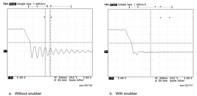
This document describes the design of a simple “RC snubber circuit”. The snubber is used to suppress high-frequency oscillations associated with reverse recovery effects in power semiconductor applications
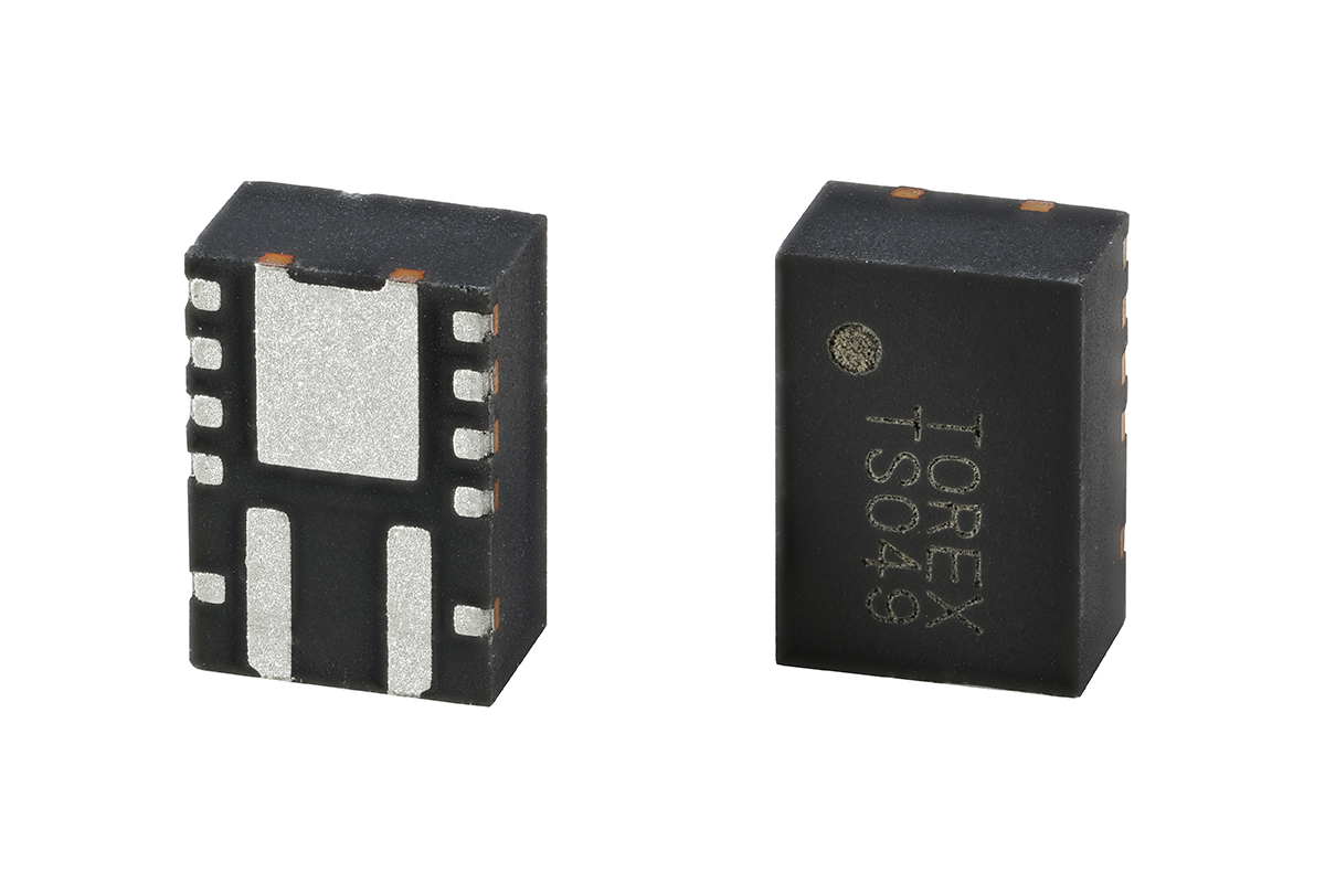
Torex Semiconductor Ltd. has launched the XDL605/XDL606 series of AEC-Q100 compliant, ultra-small step-down “micro DC/DC” converters which have an integrated coil and control IC.
A DC/DC converter power supply circuit can be constructed simply by adding a ceramic capacitor and a resistance for voltage setting to the external components, which can contribute to substantially reducing space requirements for board areas and shortening development periods. Also, the internal incorporation of the coil simplifies board layout, making it possible to minimize radiation noise and problems with circuit operation.
An input voltage of 3.0V to 36V (absolute maximum ratings 40V) with a switching frequency of 2.2MHz, 0.75V standard voltage supply are built-in, and the output voltage can be set from 1.8V to 5.0V with an external resistance. The control system can be selected from PWM control (XDL605) or PWM/PFM automatic switching control (XDL606).
The soft-start time has been internally set to 2.0ms (TYP.), but can be optionally set to any desired value by connecting a resistance and capacity to the EN/SS pin, and the power good function makes it possible to monitor the status of the output voltage. Sequence control can be performed with a combination of the softstart time and power good function.
The coil and control IC are encapsulated in a DFN3625-11B ultra-small leadless package (outside dimensions: 2.5 x 3.6 x h1.55mm) (Figure 1), making these products among the world’s smallest class of coilintegrated DC/DCs compliant with AEC-Q100.
Furthermore, the package uses a wettable flank structure, and fillets are formed at the side of the terminal by this, allowing automatic visual inspections of solder joints to be performed.
The product series also has a line-up of conventional DC / DC converters with an external coil which are XD9267 / XD9268 series. With two different solutions available of stand-alone DC/DCs and coil-integrated, customers can select the best solution to match their own unique applications.
This module is a non-isolated 7A DC-DC converter. The module can convert any DC voltage between 7V to 50V to a 5V DC with load current up to 7A. The project has been designed around LM5116 Wide Range Synchronous Buck Controller IC. The design includes 6uH toroid inductor and two N channel MOSFETS. The operating frequency is 250 KHz.
The LM5116 is a synchronous buck controller intended for step-down regulator applications from a high-voltage or widely varying input supply. The control method is based upon current mode control utilizing an emulated current ramp. Current mode control provides inherent line feed-forward, cycle-by-cycle current limiting, and ease-of-loop compensation. The use of an emulated control ramp reduces noise sensitivity of the pulse-width modulation circuit, allowing reliable control of very small duty cycles necessary in high-input voltage applications.
The operating frequency is programmable from 50 kHz to 1 MHz and the LM5116 drives external high-side and low-side NMOS power switches with adaptive dead-time control. A user-selectable diode emulation mode enables discontinuous operation mode, for improved efficiency at light load conditions. A low quiescent current shutdown disables the controller and consumes less than 10 µA of total input current.
Additional features include a high-voltage bias regulator, automatic switch-over to external bias for improved efficiency, thermal shutdown, frequency synchronization, cycle-by-cycle current limit, and adjustable line under-voltage lockout. The device is available in a power enhanced HTSSOP-20 package featuring an exposed die attach PAD to aid thermal dissipation.
Since the recent move by Espressif Systems to go into mass production of the ESP32-S2 SoCs, modules and development boards, we have been seeing quite a number of arrivals from the company, one of which was the very first ESP32-based development board, the ESP32-S2-Saola-1 development board which started selling on Mouser and digikey for $8.
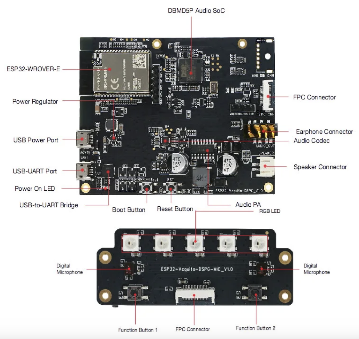
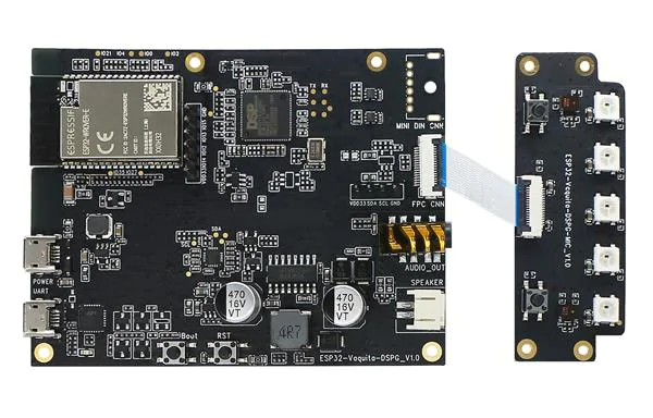
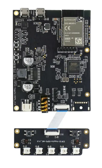
Again, the company has announced the arrival of a new ESP32-based development board with SDK for building voice-controlled IoT devices with core cloud service. The ESP32-Vaquita-DSPG development board is a certified solution that offers an easy, cost-effective and secure way to develop Alexa built-in smart devices with Alexa Voice Service and AWS IoT-cloud connectivity.
The board amongst others, has an Espressif’s ESP32 wireless ESP32-WROVER-E module, DSP Group’s DBMD5P Audio SoC and two Mic solutions with Acoustic Echo cancellation and beamforming. The wireless module comes embedded with ESP32-D0WD-V3, WiFi and Bluetooth connectivity, 64 Mbit SPI flash and 64 Mbit PSRAM for flexible data storage while the DBMD5P Audio SoC has far-field voice recognition enabled by the company’s HDClear algorithms.
The ESP32-Vaquita-DSPG board also has an Audio Codec ES8311 that communicates with ESP32 to convert digital signals to analog signals and an audio Power Amplifier for external speakers up to 8W. It is the combination of this board with a companion phone app SDK that makes developing Alexa built-in IoT devices with Alexa Voice Service and AWS IoT-cloud connectivity easy, cost-effective and secure.
Other features of the board include:
FPC connector
2 digital microphone arrays on MIC board
Speaker and earphone connectors
USB-to-UART port
5V power supply input via USB Power port
3.5mm audio jack
Power On LED, 5x RGB LEDs
Boot & Reset buttons, 2x function buttons
5V-to-3.3V power regulator
For hardware setup, you will need :
computer running Windows, Linux or macOS,
pair of headphones or an external 4-ohm speaker for audio output and
2 cables for power and debugging.
Meanwhile, the SDK, on the other hand, provides production-ready sample codes for full AVS for AWS IoT SDK functionalities like WiFi configuration, music service, and Amazon Login functionality through open-source phone apps for Android and iOS.
For now, the ESP32-Vaquita-DSPG development board appears to be available only on Mouser and it is being sold for $45. Hopefully, with time, the board will begin to appear on the sites of other resellers. More details on getting started with the development board as well as the schematics, PCB layout and BoM can be found in the user guide here.
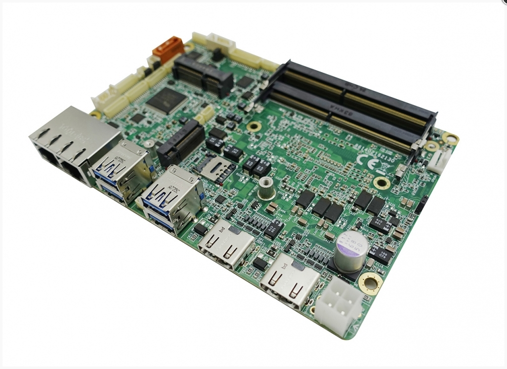
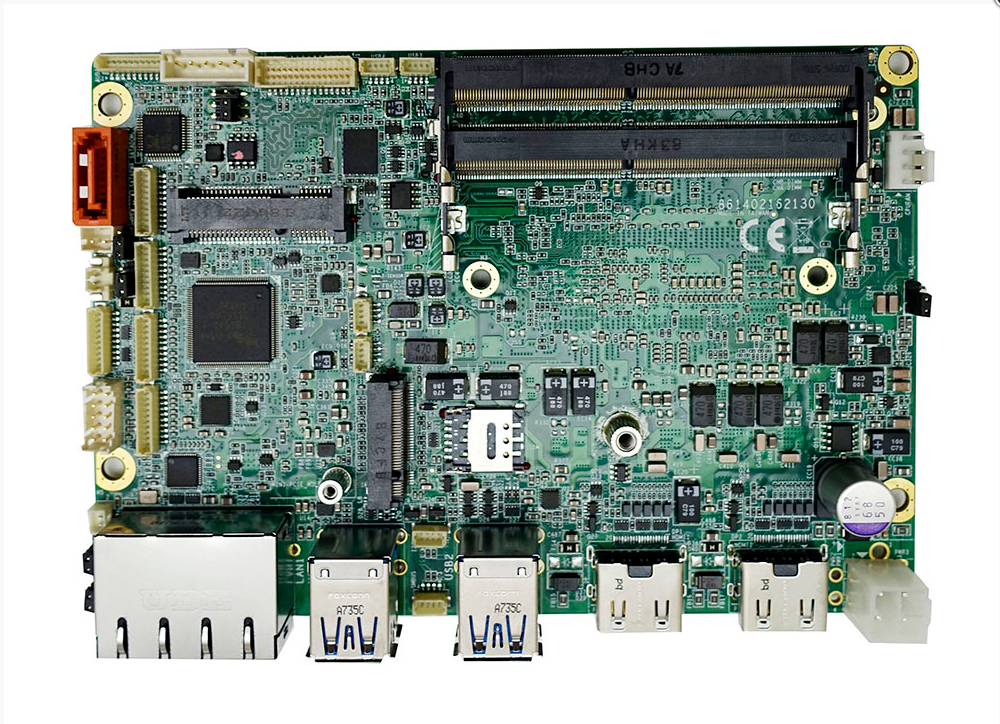
Intel® Whiskey Lake-U® Series based 3.5″ Embedded Board support Intel® 8th Generation CoreTM i7/i5/i3/Celeron® Processor with DP(HDMI)/ LVDS(eDP), SATA III, 4 COM, 6 USB, Dual Intel® GbE LAN..
Litemax is unveiling a 3.5-inch embedded board, AECX-WHL0, based on Intel 8th generation Core processors. The AECX-WHL0 is powered by 8th Generation Intel Core i3/i5/i7 and Celeron processors (codename Whiskey Lake).
The AECX-WHL0 provides various I/O features including six USB ports, two Gigabit Ethernet ports, and up to four COM ports. The AECX-WHL0 also offers display ports, featuring two DP or HDMI and LVDS. Users can also make use of the AECX-WHL0 with a full-sized Mini-PCIe slot and multiple M.2 slots (one 2280 M-Key and one 3042 B-Key).
According to the company, the AECX-WHL0 is built to power embedded applications wherever it’s deployed. Designed for tough conditions, it features wide voltage input as well as a wide operating temperature range.