NEXCOM, the leading provider of network communication appliances and uCPE, introduces the NSA 6310, based on NXP® Semiconductors’ latest multi-core Layerscape® LX2160A platform. The NSA 6310 offers better performance and pricing than the market’s existing solutions and also fulfills telecom and IoT operators’ demand for multi-technology and edge computing white box solutions to address operational environment and business needs.
“Edge computing is key to pushing next-gen networks to deliver better user experiences with low latency and high performance. The NSA 6310 with ARM platform is low cost while providing high performance and additional PCIe I/Os to add FPGAs or GPUs for AI/ML services in the edge,” explains Jovanni Lee, V.P. of Network & Communication Solutions at NEXCOM. “We are proud to deliver ARM edge computing by working with NXP.”
“With one of world’s most comprehensive edge computing portfolios today, NXP continues to play a leading role in developing the ARM-based hardware and software ecosystem. By leveraging our hardware-accelerated, Layerscape family of multicore processors, NEXCOM is expanding the availability of advanced uCPE solutions that can enable high-performance, low-power virtualized solutions,” Noy Kucuk, vice president product management, Digital Networking, NXP. “As a result of our collaboration, these differentiated uCPE offerings are designed to enable service providers to deploy efficient, edge compute systems that can support high-performance, multi-cloud frameworks.”
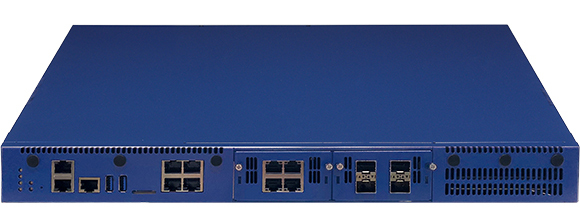
NEXCOM’s NSA 6310 is an open uCPE based on the Layerscape® LX2160A processor, with sixteen 64-bit ARM Cortex-A72 cores. The cores, in combination with integrated hardware acceleration for cryptographic processing, virtual forwarding, and traffic management, provide support for multi-gigabit routing and network services.
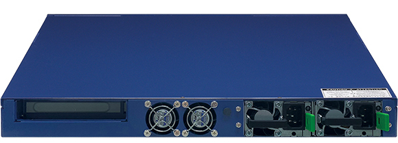
The NSA 6310 white box also offers two SerDes slots, with a choice of four dedicated 25G, 10G, and 1G LAN modules, for customers who need multiple I/Os to satisfy different applications; FPGA/GPU support to extend computing applications, board manager control (BMC) module and IEEE 1588 PTP feature for server-grade network appliances; and optional PoE support for edge deployments.
Main Features
NXP® Layerscape® LX2160A SoC, BGA type
4 x DDR4-3100 ECC-DIMM
1 x 2.5 SSD, 1 x M.2 2280
PCIe Gen3 x8 with SR-IOV
Dual boot device
Enhancing UEFI
Support secure boot and optional TPM
2 x SerDes LAN modules support 25G/10G/1G
4 x GbE RJ45
Optional IEEE1588 PTP
Optional BMC support with manager port
Redundant power supply
Optional PoE at/af support
Operating system: NXP® LSDK (Ubuntu userland)
No pricing or availability information was provided for the “coming soon” NSA 6310. More information may be found in Nexcom’s announcement and product page.
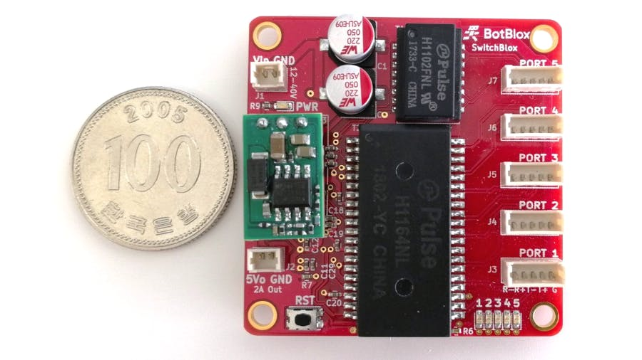
SwitchBlox is an open-source ethernet switch designed by Josh Elijah, who is the founder of BoxBlox. It was designed to make life easier for robot and drone developers or anyone who needs to use an ethernet switch. The switch is tiny, thereby making it easy to use in size constrained areas.
According to Josh,
” there’s currently no option for robot and drone builders looking for small and robust ethernet switch that is also open source.” The SwitchBlox is a 10/100 ethernet switch that is complete and fully available with a Creative Committee License. SwitchBlox offers a way to “incorporate Ethernet into space, weight, and power-constrained applications easily.”
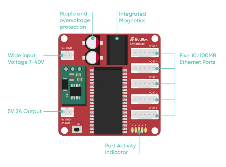
Despite having its dimensions as 44.5 mm by 44.5 mm (1.75 by 1.75 inches), the switch has five Ethernet ports and still has room to display the LED status readouts for each of the ports. Due to its small size, there are no RJ-45 ports on the SwitchBlox. 1.25 mm Molex Picoblade five-way connectors that break out to RJ-45 with bundled cables are provided as a replacement.
BoxBlox’s Open Source Ethernet Switch Offers Five Ports
Also, other cables are available with un-terminated ends. They can be used for power input, manual wiring, and or output. An extension cable kit which costs £29.00 is being sold. It is optional and provided just in case the user needs more cables.
The SwitchBlox can be used straight out of the box as an unmanaged switch. Users should simply apply a 7 to 40 V DC supply and connect devices using cables provided. The switch will start forwarding packets almost immediately without any setup.
While SwitchBlox caters to the needs of users seeking simplicity and efficiency in network deployment, other options in the market, such as the aruba unmanaged switch series, offer additional features and scalability for larger-scale applications. Despite their differences in functionality and capabilities, both SwitchBlox and Aruba switches share a common goal of providing reliable and straightforward networking solutions.
Whether opting for the compact form factor of SwitchBlox or the robust feature set of Aruba switches, users can rest assured that they are investing in hardware designed to simplify network connectivity and enhance productivity.
Another option available is the use of an SPI (Serial Peripheral Interface) bus to access and implement full capabilities. This can be used when dealing with advanced applications. However, it is important to remember that the board comes fully assembled and can be used without firmware.
Other features include the Auto MDI-X crossover and a 5V 2A power output connector to provide power to additional hardware.
Further Information and Pricing
“I haven’t closed off the design. I want this to help robot and drone developers and eventually build a suite of open source networking hardware for robots and drones,” said Josh. The SwitchBlox cost £149.00 with VAT and £124.17 without VAT on BoxBlox and $155 on Tindie. Some files for hardware in Ki Cad can be found on the BoxBlox GitHub repository. Firmware files and Software files will be in C++ and Python, respectively. The former and latter will soon be posted on the same repository.
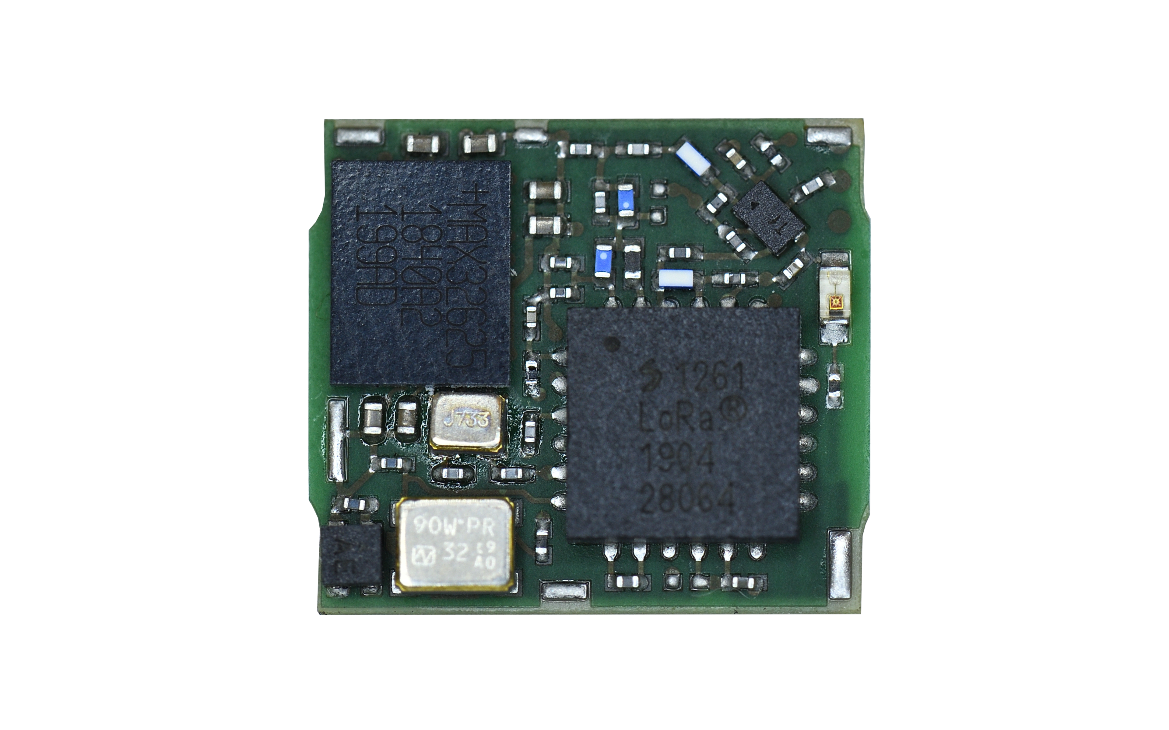
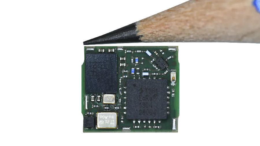
Miromico AG has developed a LoRaWAN module with integrated Arm Cortex-M4microcontroller, which was unveiled at Embedded World 2020. They claim it is the world’s smallest LoRaWAN module with integrated Arm Cortex-M4 microcontroller. Also referred to as the FMLR-6x-x-MA62x Module, Miromico module’s latest design is built around the Maxim MAX23625/26 microcontroller, which enables an Arm Cortex-M4, clocking at up to 96MHz from the internal oscillator of as low as 4MHz from a low-power system clock.
The LoRa® FMLR RF modules enable wireless connectivity to almost all devices, systems and sensors communicating at low data rate over a distance of more than 50km. It is equipped with the latest software “LoRa Basics™ MAC”. Power consumption of the underlying nodes can be optimized to run from a small-sized battery, while the integrated radio allows the system to operate in a duty-cycled manner. It also offers 512kB of flash memory, 160kB of static RAM, 9kB of instruction cache, and extremely low power operation, which goes as low as 49µA/MHz when executing from flash and 2.56µW in data-retaining sleep mode. The module features wireless connectivity, which is enabled via a Semtech SX1261 or SX1262 wireless transceiver, offering full support for the increasingly popular LoRaWAN low-power long-range wide area network protocol with up to 20dBm transmission and -137dBm receive sensitivity.
In order to enable backward-compatible upgrade paths for grown products and systems, the FMLR family supports additional modulation schemes over LoRa. These modulation schemes include (G)FSK, (G)MSK, ASK, and OOK. Highly configurable OTA packet formats enable the communication with standards like Wireless Mbus and IEEE802.15.4g. The modules also allow the emulation of proprietary systems such as Nordic NRF905 or NRF9E5 with enhanced coverage range. For fast prototyping and development, the proprietary firmware including the wireless stack can be updated via SWD, UART-Bootloader, or OTA. Measuring 8.6mm by 9.3mm (around 0.34″ by 0.37″) in size, Miromico claims the module as “to the best of our knowledge the smallest LoRaWAN module ever produced.” For it to be easy to use during the prototyping stages, a daughterboard is available, which adds a Hirose U.FL antenna connector, additional external flash storage, and extra sensors. The LoRaWAN software stack is available as an open source solution which runs on the integrated microcontroller.
Even though Miromico has unveiled the module and daughterboard at Embedded World, the module is not quite ready to be put up for sale: The company however says they will only be distributing the module and a compatible starter kit to “alpha clients,” with no information about commercial availability. More information may be found on the company’s official product page.
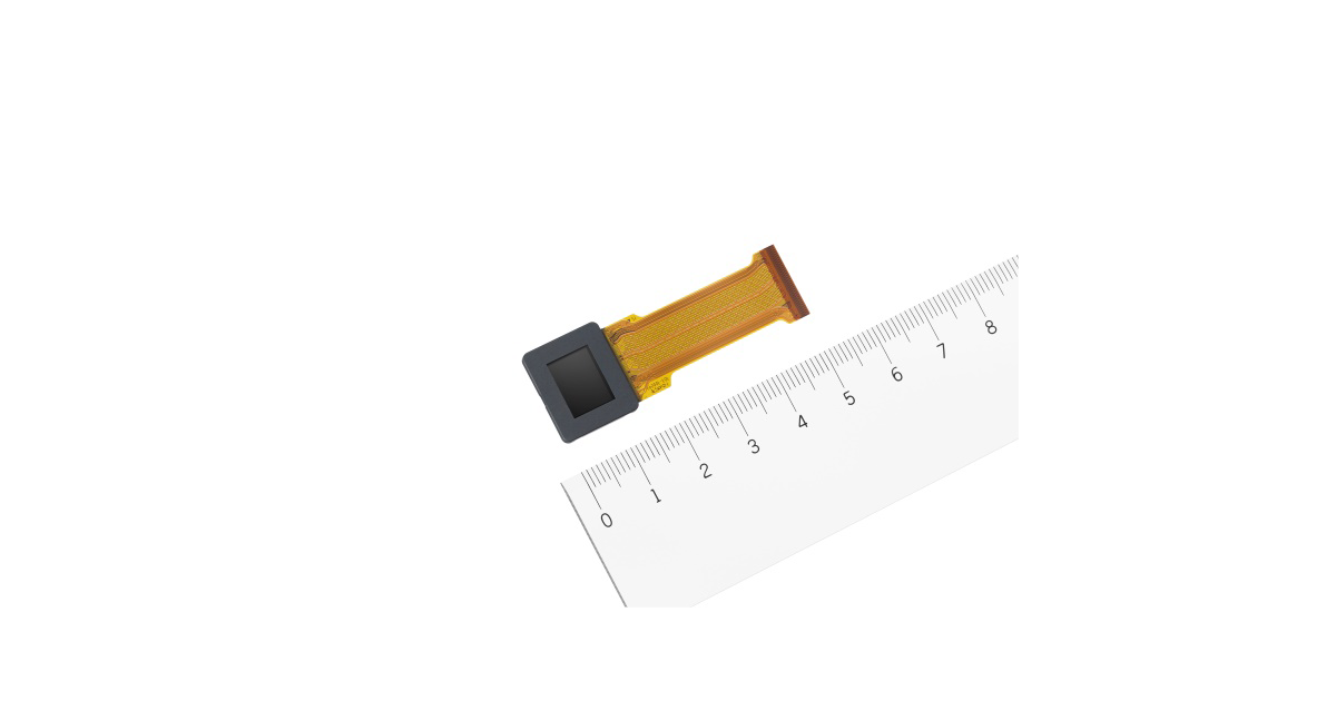
FRAMOS, a global partner for vision technologies, now offers the new ECX335S microdisplay series from Sony Semiconductor Solutions. Featuring outstanding brightness, contrast and resolution plus a wide viewing angle, this solution is suited to the fast-growing market of augmented reality (AR) devices. These include head-mounted displays (HMDs), electronic viewfinders (VFs), and small monitors. The ECX335S is an OLED panel module with active matrix color design, exceptional brightness of up to 3,000 cd/m², Full HD resolution with 1,920 x 1,080 RGB pixels, and a diagonal of 1.8 cm (0.71 inch). Its power consumption is low even at a frame rate of 60 fps.
AR applications require brightness in excess of 1,000 cd/m². This means the OLED microdisplay must have a nominal value of at least 3,000 cd/m², to allow for transmission losses during projection. Through a clever combination of enhancements, Sony Semiconductor Solutions has increased the brightness of the new ECX335S microdisplays by a factor of three compared to previous models, while maintaining the same operational life. With its brightness characteristics, extremely small form factor (21.44 mm x 15.62 mm) and a contrast ratio of 100,000:1, this module will continue to spur innovative AR solutions. Information levels in the HMD or VF are rich in contrast and blend seamlessly into the real world, creating a “real” AR experience.
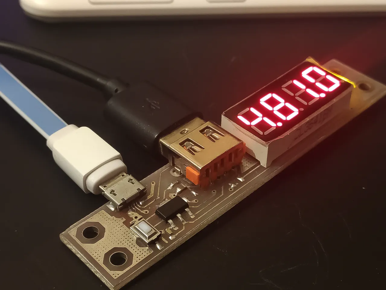
With a code size of 1KB on an ATtiny13A MCU, this tiny module measures voltages up to 22 volts and current up to 5 amps. This project is published by Tirdad Sadri Nejad. He writes:
There are a lot of so-called “USB doctor” modules which are used for monitoring currents flowing through a USB connection. They are used for cable or charger testing, quick charge detection and load current consumption measurements. They’re cheap of course and someone may ask why should we build one? If you can do it better, then do it. So what’s better about my design?
Self-calibration: You don’t need to know the exact resistor values used for voltage dividers. Just use a proper divider to map your desired voltage range into 0~1.1v range (1.1v is the internal V-ref of ATtiny13. The feature we needed it for). after that all you need to do is to connect the module to a precise 5v supply while holding the onboard button. the device starts up and shows “C” character on the display, calculates the divider values itself and saves them in the internal e2prom. So you just need to do it once.
Various display options: Using the button, you can switch between current display, voltage display and both. It is possible to save the preferred display on e2prom for startup.
A 1KB code challenge: Despite there are better options than using 2 chips (1 micro controller + 1 display driver), I like the discrete designs. I had to implement a display library too. The display driver is universal and you can use it for any other microcontroller that supports an ANSI C compiler! read the libraries provided below.
The design is based on an ATtiny13A microcontroller, a TM1637 LED driver and a 0.033ohms current sense resistor. the 1.1v ADC voltage reference on the ATtiny came quite handy for better precision.
I had to get rid of floating-point calculations. despite the voltage divider and the values shown on the display may seem to have radix points, they don’t. The values are calculated as mA and mV and then a point is placed in the display at proper location. so there was no need to calculate float values.
Self-Calibrating USB Voltage/Current Meter – [Link]
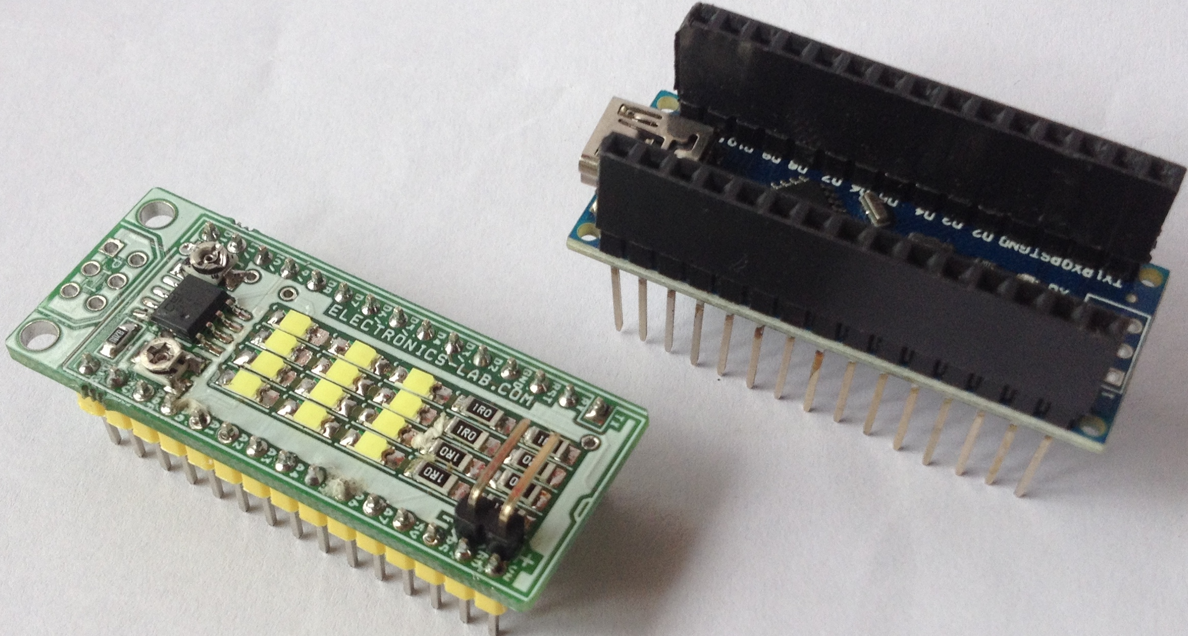
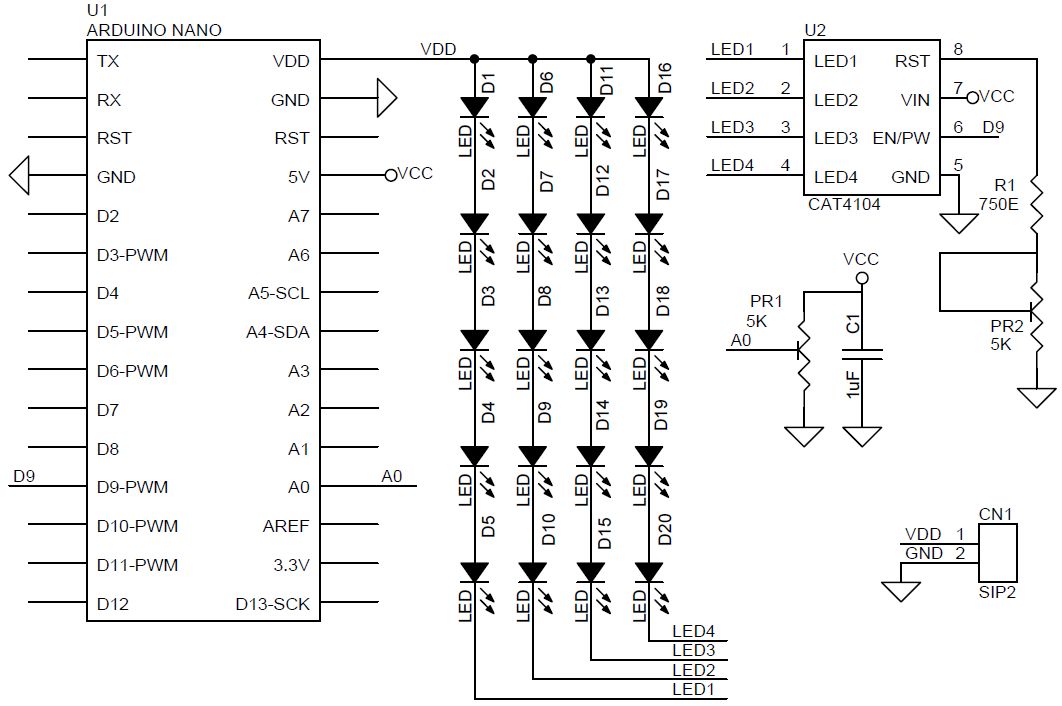
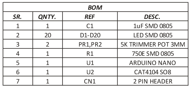
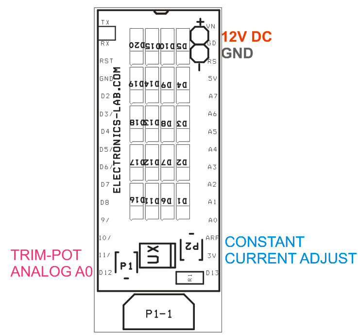
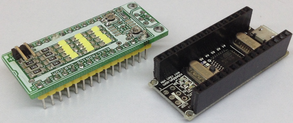
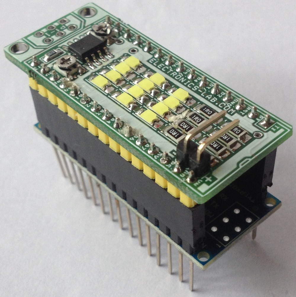
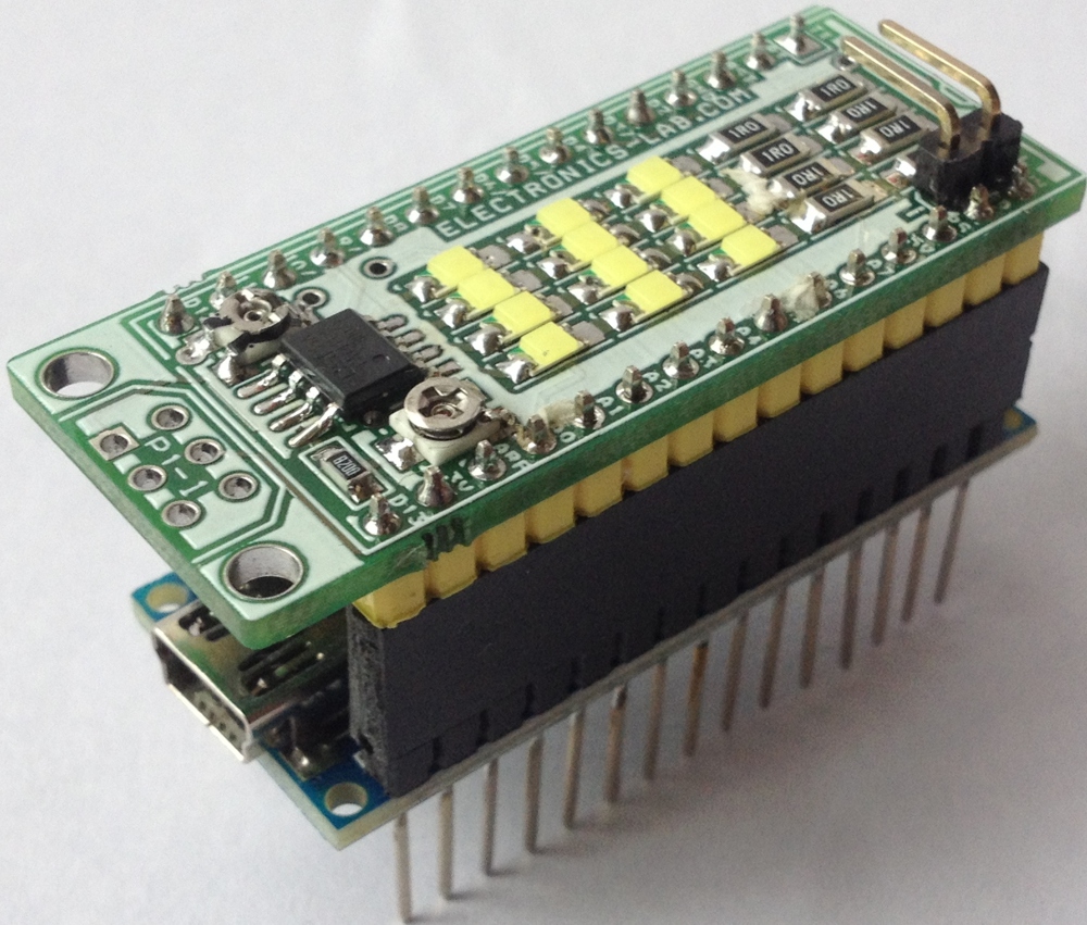
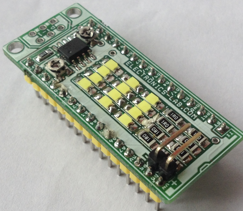
This small constant current LED driver Nano shield has been designed using CAT4104 IC from ON semiconductor. Its 4 channel LED driver. The board has provision to mount 20 SMD 1206 LEDs. The LED can be RED, GREEN, BLUE and WHITE. Reduce the number of LED to 12 if White LEDs are used, as white LEDs are 3-5V and total series voltage should not exceed 12V. CAT4104 provides four matched low dropout current sinks to drive high−brightness LED strings up to 175 mA per channel. The LED channel current is set by an external trimmer potentiometer connected to the RSET pin. The LED pins are compatible with high voltage up to 12V. The EN/PWM logic input supports the device enable and high-frequency external Pulse Width Modulation (PWM) dimming control. Thermal shutdown protection is incorporated in the device to disable the LED outputs whenever the die temperature exceeds 150°C. Nano LED shield can be used to develop intelligent lighting for Automotive and Architect since PWM pin of LED driver connected to D9 PWM pin of Arduino. The EN/PWM pin has two primary functions. One function enables and disables the device. The other function turns the LED channels on and off for PWM dimming control.
The device has a very fast turn−on time (from EN/PWM rising to LED on) and allows “instant on” when dimming LED using a PWM signal. Accurate linear dimming is compatible with PWM frequencies from 100 Hz to 5 kHz for PWM duty cycle down to 1%. PWM frequencies up to 50 kHz can be supported for duty cycles greater than 10%. PWM pin connected to D9 of Arduino.
Note: Replace D1, D6, D11, D16, D2, D7, D12, and D17 with 0 Ohms SMD 1206 Resistor in case of white LED used.
Features
Input supply 12V DC
LED Load 750mA (4 Channel)
Constant Current Adjustable with help of Trimmer Potentiometer
Thermal Protection Shutdown
PR2 Trimmer Pot Provided to Adjust the Constant Current 80mA to 750mA
D9/PWM Of Arduino Connected
PR1 Trimmer Pot Connected to A0 Pin of Arduino Nano for Dimming Application
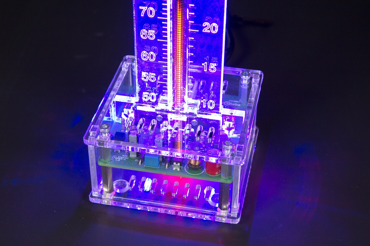
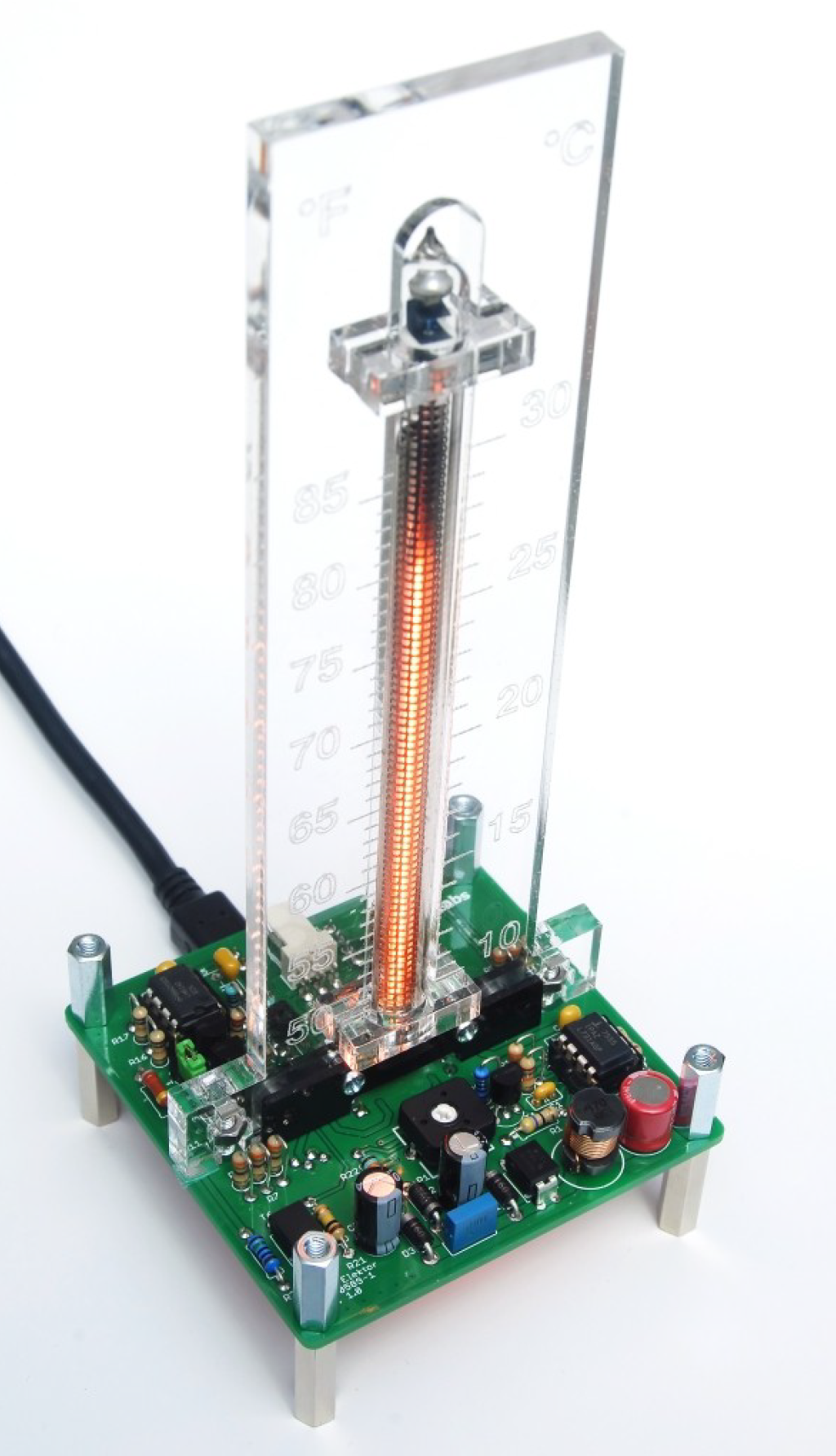
Nixie tubes are always fascinating. Nowadays they are mostly used for clock displays, such as the project in the May/June 2016 issue of Elektor. The ‘Nixie’ bargraph tubes for analogue readout in the form of a column of light are less well known. Strictly speaking, they are not Nixie tubes because they do not display numerals, but they have the same warm retro allure because they are also filled with neon gas. The thermometer described here uses a Russian IN-9 tube and is a nice alternative to the usual clock projects.
Original publication: Elektor Magazine 5/2018 (July & August) on page 30
Author: Ilse joostens
Original article production number: 160705
Semi kit available, see PRODUCTS below
Free download expires: Friday 27 March 2020
Like what you’re seeing? Then go to the article page and download a pdf copy of the full, original article. Downloading is free from Friday 20 March to Friday 27 March 2020.
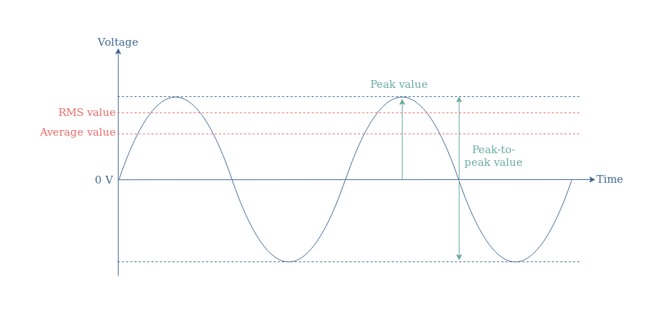
In the DC regime, only one definition of the value of a voltage is possible, this value is unambiguous and is determined by the difference between the reference value 0 V and the flat line figure of the DC signal.
In the AC regime, however, it can lead to confusion to speak of only one value for the voltage. From a simple sine waveform, we can at least list indeed four different definitions of voltage:
fig 1: Illustration of the peak, Average and RMS values
The peak value corresponds to the difference between the reference (which is the value where the AC signal oscillates around) and the maximum value of the signal. The peak-to-peak value is the peak value multiplied by a factor 2, it corresponds to the total vertical width of the signal.
In Figure 1, we have also highlighted the Average and RMS values in red, which we will be focusing on in the following of this tutorial.
The two sections developed in this article will separately present the Average and RMS values, we will see how they are defined, how to determine them and finally we will see what is special about the RMS value.
Average Voltage
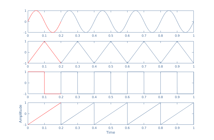
For an elementary symmetrical sine, triangle, square or sawtooth waveform (see Figure 2 and AC Waveform tutorial), it is unclear to speak of the average voltage value, that we will note A in the following. Indeed, these types of signals are during half of their period positive and negative during the other half. In other words, the signals are 50 % of the time above the horizontal axis and 50 % under it.
From that observation, it is easy to understand that if we consider the average value of any of these signals on a full period, it is equal to 0, regardless of the peak value, and therefore not relevant.
fig 2: Elementary sine, triangle, square and sawtooth waveforms
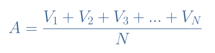
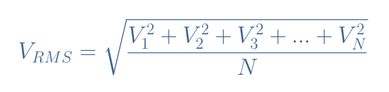
We can demonstrate this result by explaining how to calculate the average value. For a finite set of values, the averaging process consists of summing all the values (V1, V2, V3…) and dividing them by the cardinal number N of the set (how many values there are in the set):
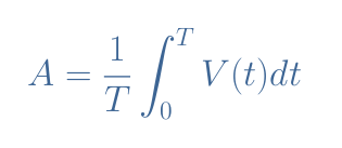
For an analog signal, however, it is impossible to sum all the instant values, also called mid-ordinates, that the signal takes during a period simply because there is an infinity. Instead of summing, we use the integration operation:
eq 1: Average of an AC signal V(t) taken for a full period
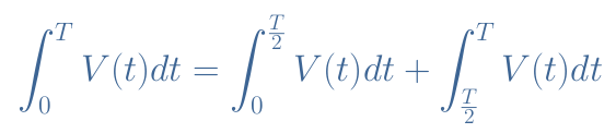
Equation 1 is the average of the signal V(t) taken between the times 0 and T, that is to say, a full period. The term ∫V(t)dt gives the value of the area between the curve V(t) and the reference of 0 V. Because the integration operation is linear, this term can be split in two:
For an elementary waveform such as presented in Figure 1, we can see that the first and second terms of this formula are equals but of opposite signs, therefore the average value is equal to 0.
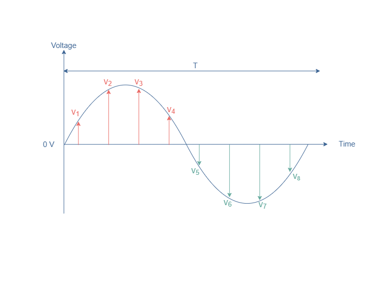
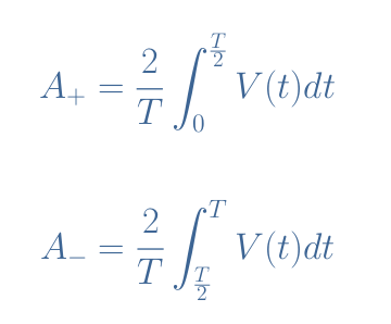
In order for the average value of such signals to make sense, we prefer to consider separately the half positive and negative periods, which some their values are respectively highlighted in red and green in the following Figure 3:
fig 3: Some instant-values for the positive half-period (in red) and negative half-period (in green) of a sine waveform
Similarly to Equation 1, we can define separately the average values for the positive half-period (A+) and negative half-period (A–):
eq 3: Averages of an AC signal V(t) taken for the positive (+) and negative (-) half-periods
The value of A+ and A– depends on the signal we are dealing with and their respective peak values (Vp). We list below the absolute value |A| of A+ and A– for the most common elementary and symmetrical AC signals:
Sine waveform: |A|=0.637×Vp
Triangle waveform: |A|=0
Square waveform: |A|=Vp
Sawtooth waveform: |A|=0.5×Vp
We can conclude this section by saying that when we want to average a signal, we need to give the precision if the process is done on a full period or a smaller value. For the elementary and symmetrical AC signals, averaging on a full period always gives the result 0 V regardless of the frequency, peak value or period. For this reason, it is more appropriate to average these signals during their half-periods.
RMS Voltage
RMS stands for Root Mean Square, is it a similar operation to the average value presented previously but the instant values are instead squared and the total fraction is rooted:
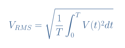
For the same reasons as stated previously, we use the integration operation to define VRMS for an analog signal:
eq 4: RMS value of an AC signal V(t) of period T
Unlike the average value, the RMS value is always defined for a full period of the signal, there is indeed is no possible confusion to determine this value.
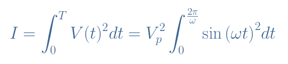
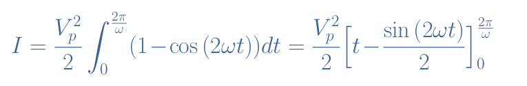
As an example, let’s determine the RMS value of a sine waveform of peak value Vp and angular pulsation ω V(t)=Vp×sin(ωt). We note f the frequency that satisfies f=ω/2π and T=1/f the period.
First of all, we compute the integral term that we note I:
We use the trigonometric identity sin2(x)=(1-cos(2x))/2 to continue:
Evaluating the bracket term between 0 and T gives 2π/ω=T. Therefore, the integration term is finally equal to (πVp2)/ω. From Equation 4 we can see that we still need to multiply by 1/T which leads to [(πVp2)/ω]×[ω/(2π)]=Vp2/2 for the term under the root.
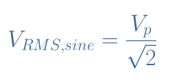
Finally, after taking the root, the final expression for the RMS value of a sine waveform is given by:
We list below the RMS values that can be computed by the same method as the sine example above for the elementary and symmetrical signals stated in the previous section:
Sine waveform: VRMS=Vp/√2
Triangle and Sawtooth waveform: VRMS=Vp/√3
Square waveform: VRMS=VP
It is important to note that VRMS>|A|, the RMS value is always greater than the absolute value of the average.
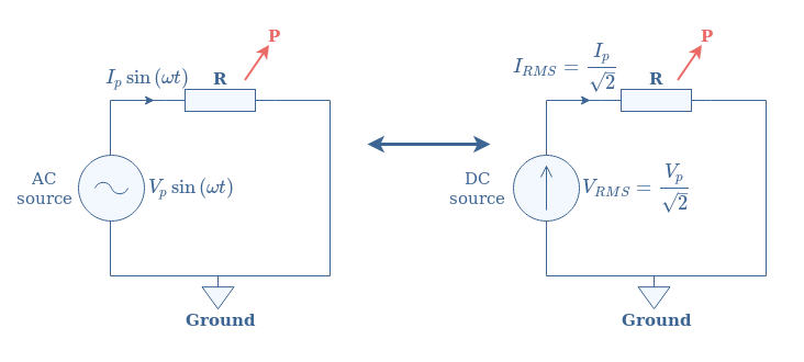
What is fundamental to understand the RMS value is that it creates a link between the DC and AC regimes according to the following Figure 4:
fig 4: Similarity between the AC and DC regimes
The RMS values of voltage and current are the values that develop the same power across a resistance in a DC regime.
Conclusion
The average and RMS values can easily be measured by modern voltmeters or oscilloscopes and provide information about an AC signal.
The numerical approach for the average consists of summing all the values of a signal and divide the sum by the number of values. For real signals, we prefer to use the integration operation which is an extension of the sum for an infinite set of values.
Two definitions are possible for the average value, depending on if the average is done on a full period or a half-period. Symmetrical signals are characterized by an average value of 0 on a full cycle. The average value on a full cycle is different from 0 only if a DC component is present in the signal or if the signal is not symmetrical around a horizontal reference. Averaging on a half-period can also be done in order to characterize differently symmetrical signals.
The RMS value is defined similarly to the average value but each value of the sum is instead squared and the final result is rooted. The root-mean-square value is always higher than the absolute value of the average and established a link between the AC and DC regimes, which is why it is particularly used by engineers.
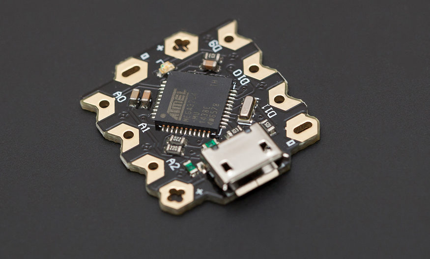
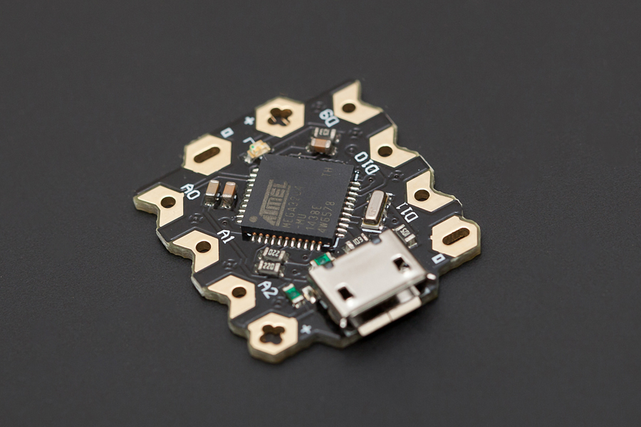
Beetle is one of the smallest Arduino Leonardo board. It derives its core notion from minimalism without compromising functionality.
It comes with Atmel AtMega32u4 ( datasheet) @16MHz clock time and has expanded amounts of interfaces: 10 digital pins, 5 analog pins, and 4 pwn pins. To further make it user-friendly, it is compatible with Micro USB so that direct programming and testing is no longer a headache. Select “Arduino Leonardo (tools >board > Arduino Leonardo in Arduino IDE), the ATmega32U4 comes pre burned with a bootloader that allows you to upload any new code that is applicable to Arduino Leonardo.
As the smallest Arduino Leonardo, it enjoys similar powerful functionalities. Beetle aims to solve problems of the low-cost controller, ease-of-using properly, and to provide a low-cost solution for disposable projects, such as DIY projects, workshops, gift projects, E-Textiles and educational. For students and makers who can not afford too much on hardware purchasing, Beetle can be a great solution for them.
Features
20mm X 22mm compact size
Direct downloading and testing via Micro USB
V-shaped large-size gold-plated IO ports make it convenient for the user to twist wires upon, and can also be directly sewn on clothes with conductive thread.
Two honeycomb shape gold-plated power interface
Magic light blue soft BLINK indicator
Specification
Microcontroller: ATmega32u4
Clock Speed: 16 MHz
Operating Voltage: 5V DC
Digital I/O Pins: 10
PWM Channels: 4
Analog Input Channels: 5
UART: 1
I2C: 1
Micro USB: 1
Power Ports: 2
Flash Memory: 32 KB of which 4KB used by bootloader
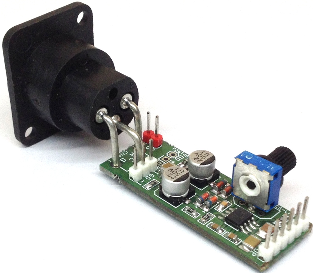
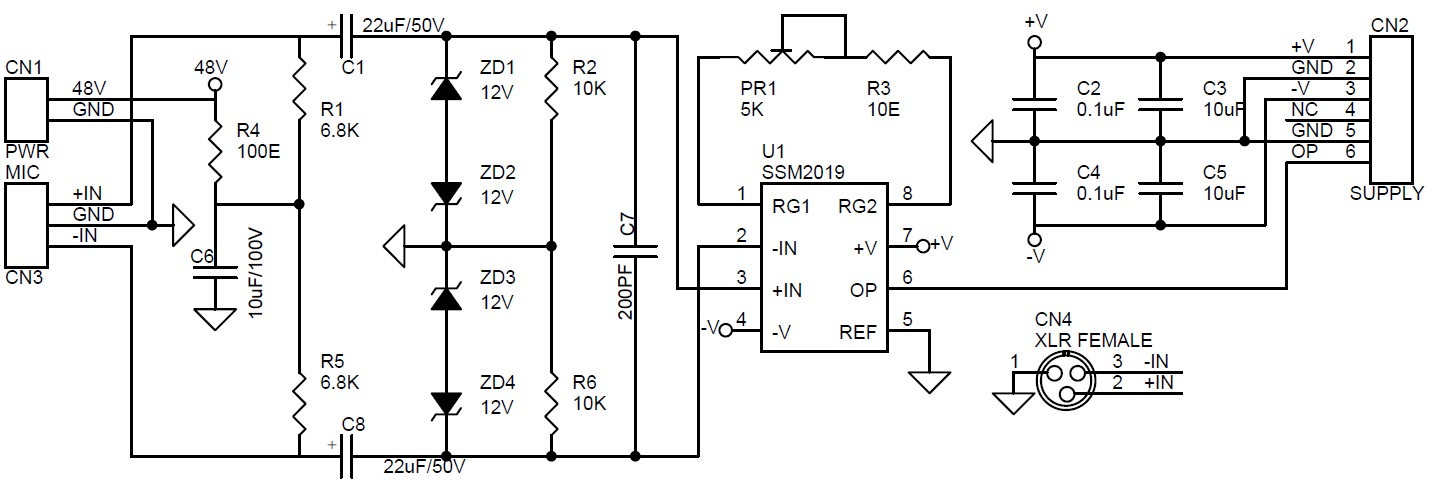
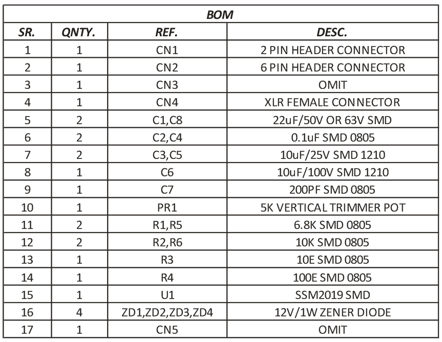
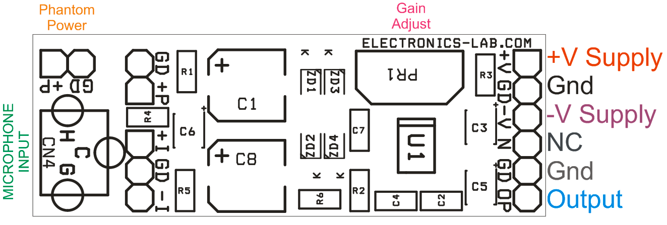
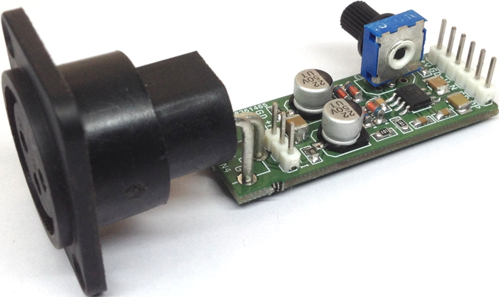
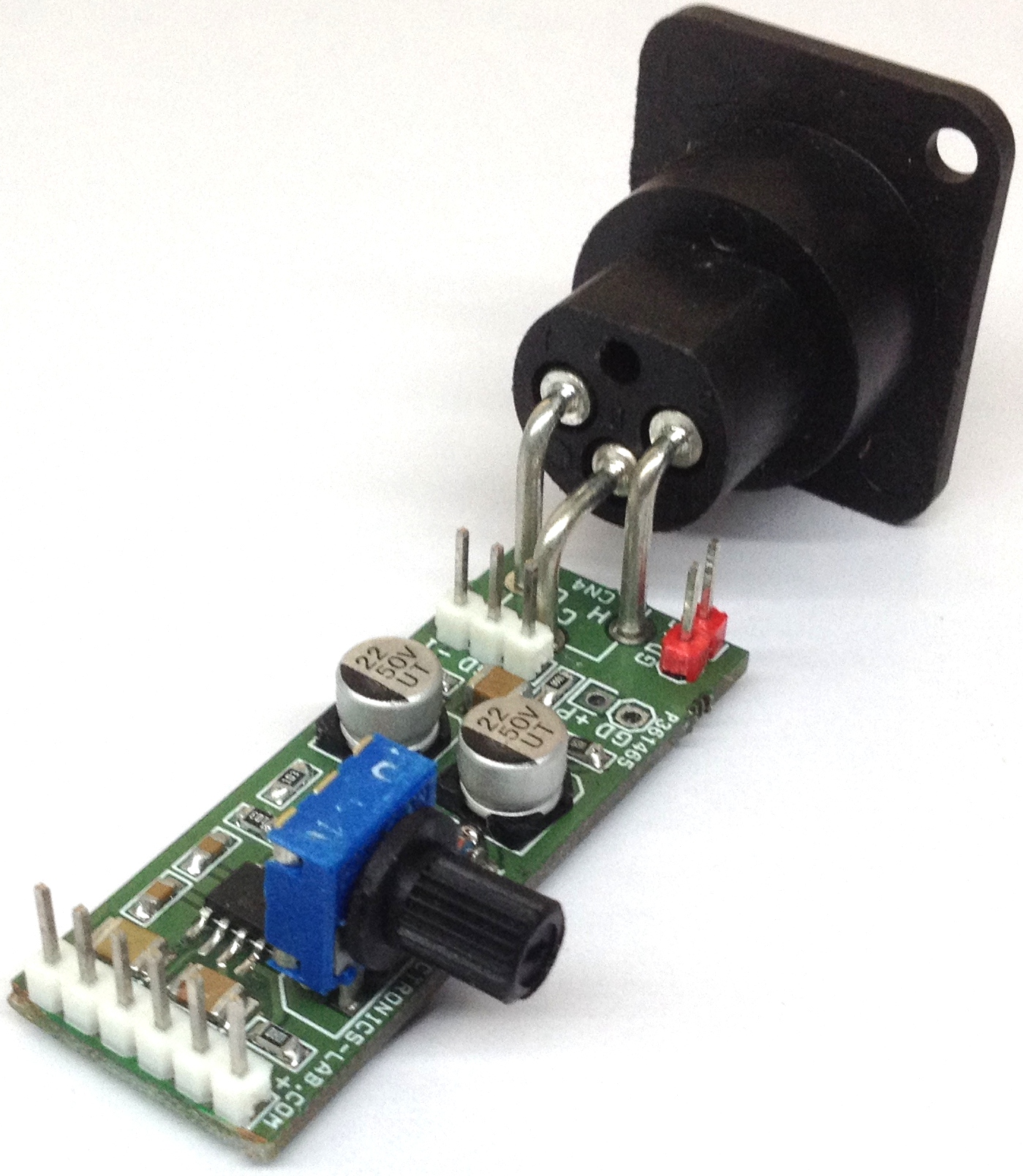
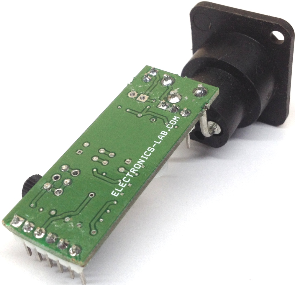
The project published here is based on SSM2019 IC which is a latest-generation Pro audio preamplifier. A female XLR connector is provided to connect differential Micro-phone. Circuit also provides Phantom power input, combining SSM preamplifier design expertise with advanced processing. The result is excellent audio performance, the attached trimmer potentiometer helps to adjust the output gain. The SSM2019 is further enhanced by its unity-gain stability. Key specifications include ultra-low noise (1.5 dB noise figure) and THD (<0.01% at G = 100), complemented by wide bandwidth and high slew rate. Applications for this low-cost device include microphone preamplifiers and bus summing amplifiers in professional and consumer audio equipment, sonar, and other applications requiring a low noise instrumentation amplifier with high gain capability. Z1 to Z4 provide transient overvoltage protection for the SSM2019 whenever microphones are plugged in or unplugged. Gain level adjustable 0 to 60dB. CN2 connector for supply input and audio output, CN4 Female XLR connector for Micro-Phone input, CN1 Phantom Power input.