Meet I-Pi SMARC, the Industrial-Ready Prototyping Platform from ADLINK

One of the major barriers to developing industrial applications is usually the complexity and cost of the development/prototyping platforms. A lot of SOMs, SOCs and board manufacturers, including ADLINK, have taken stabs at this problem with different solutions. Leveraging on the experience with their previous products, ADLINK recently announced the launch of a new product called the Industrial-Pi Smart Mobility Architecture Development Kit (I-Pi SMARC).

The Kit, according to the announcement, was designed to provide engineers/developers with an industrial-ready, low-cost prototyping platform which afforded the flexibility boards like that of the Arduino and Raspberry PI, but with features and hardening that allows it to be used-as-it-is, directly, in industrial solutions, unlike the aforementioned boards.

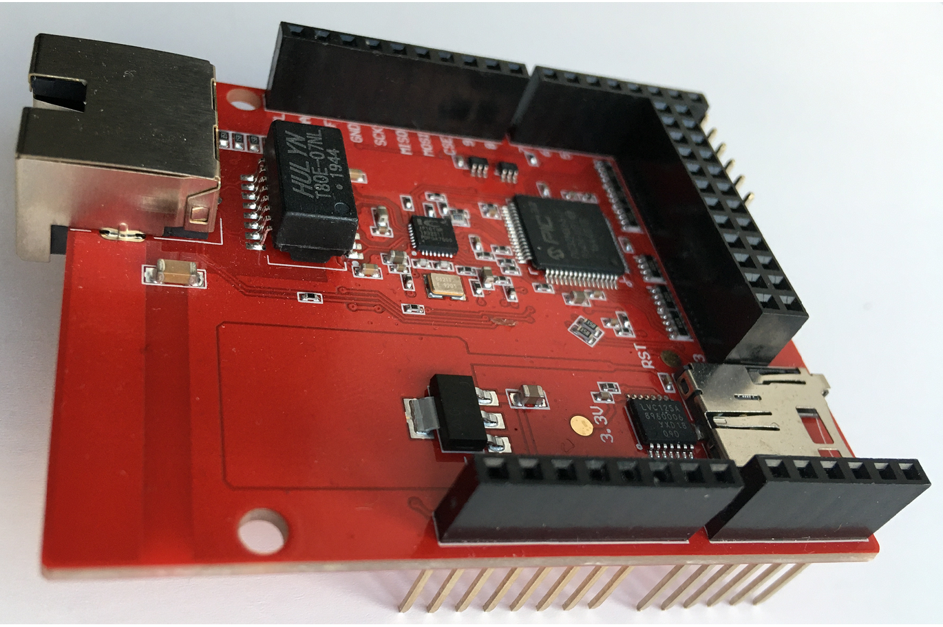
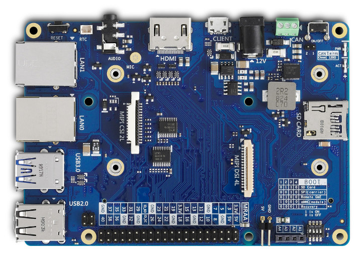
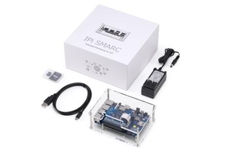
The I-Pi SMARC development kit contains an I-Pi carrier board, a LEC-PX30 SMARC module, a power supply, a USB programming cable, an SD memory card containing a Linux OS, and transparent acrylic shielding that offers protection but also ensures access to the device’s ports and IOs. The development kit is supported by the ADLINK change control process, thus it provides developers with the freedom to experiment with peripherals and sensors, and develop prototype versions of potential products with the assurance that there won’t be much to change when going from their prototype to final product.

Content of the I-Pi Kit

To make sure developing software for the SMARC is easy, the kit is supported by a hardware abstraction layer (HAL), called MRAA, and a software repository, called Useful Packages and Modules (UPM), both of which are from Intel and help streamline the software development process. The HAL (MRAA)  allows the operating system kernel to interact with the hardware in a general way, instead of at a detailed hardware level, so few or no changes are needed when kernel-mode code is run on different hardware platforms. MRAA simplifies the logic for connecting to different sensor pins and supports platforms like the Arduino and RPi along with programming languages like C++, Python, JavaScript, and Java. The UPM provides access to software drivers and libraries for a wide variety of commonly-used sensors and actuators, which are also available for Arduino and RPi platforms.

An issue I-Pi SMARC also solves for developers is the product Lifecycle management where hardware components change without substitutions being communicated to end-users, leaving commercial products built on it to rot. According to ADLINK, any component or process change to the ADLINK SMARC module will be announced in line with the industry-standard engineering and process notice (ECN and PCN) practices, with a minimum of six months before the implementation.  ADLINK guarantees 10-year availability support with after-sales support and return merchandise authorization (RMA) along with reporting and debugging on production quality issues.

Price information around the Industrial-Pi (I-Pi) SMARC kit is still a bit sketchy but you can find more information about the kit on the Announcement Page and on the recently created but seemingly empty Wiki created for it.

TI AM335x ARM SoM for Gateway Applications

MYIR introduces an Linux-ready industry-oriented MYC-C335X-GW CPU Module powered by TI’s AM335x ARM Cortex-A8 processor (800MHz AM3354 by default) which features PowerVR™ SGX530 for 2D and 3D graphics acceleration.

Measuring only 50mm by 40mm, the MYC-C335X-GW is the fourth AM335x CPU Module designed by MYIR especially for gateway applications. It integrates a DDR3L RAM memory, a Nand Flash or an eMMC Flash, EEPROM and PMIC. Two 0.8mm pitch 80-pin board-to-board expansion connectors are on the back of the module for interconnecting with a base board, thus providing an interface for the base board to carry out most of the I/O signals to and from the CPU module.

MYIR offers MYD-C335X-GW Development Board for evaluating the MYC-C335X-GW CPU Module, its base board has extended a rich set of peripherals and interfaces such as RS485, RS232, USB2.0 HOST, Gigabit Ethernet, SFP, WiFi/Bluetooth, USB based Mini-PCIe interface for 4G LTE Module, Micro SD Card slot, SIM card slot, RGB LCD and LVDS interfaces, JTAG, etc. The MYD-C335X-GW is a complete platform and solid reference design delivered with necessary accessories, detailed documentations, optional Camera and LCD modules which makes it ideal for evaluating and prototyping based on TI’s AM335x microprocessors. MYIR also offers design services to customize the base board or CPU module according to customers’ requirements.

Based on Linux 4.14.67 kernel, MYIR has provided abundant software resources including kernel and driver source code as well as MYIR’ s MEasy IOT Demo to allow customer to get a good experience and development reference.

MYIR offers below standard parts for the CPU Module, other configurations (AM335x processor, RAM, Flash, industrial or commercial grade) can be customized and the CPU Module price can be lower to $26.80/pc according to configuration and quantity.

More information about the ARM SoM can be found at MYIR’s website: http://www.myirtech.com/list.asp?id=629

High efficiency: A multi-mode, forced-frequency-resonant digital controller IC for SMPS applications

Infineon Technologies launches the XDP™ digital power XDPS21071, the first flyback controller in the industry with zero-voltage switching (ZVS) on the primary side to achieve high efficiency. This controller is aimed at fast-charging applications such as USB-PD or QuickCharge. Light-load efficiency is optimized for variable output application.

The XDPS21071 is a high-performance digital flyback controller with an integrated dual-MOSFET gate driver and a 600 V depletion startup unit. The primary-side controller drives a high-voltage external MOSFET in a flyback topology and an external low-voltage MOSFET to create a pulse for achieving ZVS condition at the high-voltage MOSFET. It supports fixed-frequency switching up to 140 kHz.

The patented forced-frequency-resonant (FFR) switching scheme is implemented by means of a digital algorithm, which is configurable via parameter settings (UART port is included) to meet application requirements and the conversion efficiency of international regulatory standards (i.e., EU CoC version 5 Tier 2 and DoE Level VI). Ease of design and system optimization are made possible thanks to the intelligent, self-adaptive multi-mode operation that matches each line/load conditions with the best-fit operational mode (i.e., FFR, CrCM, burst mode) for unparalleled system performance. Hereby ZVS operation enables for lowest switching losses. Highest system performance is achieved by only a minimal adder in BOM cost. This controller comes with adaptive overcurrent protection. It is lead-free and RoHS compliant.

45 W USB-PD SMPS reference design with XDPS21071.

Availability

The XDPS21071 in DSO-12 SMD package is now available. In addition to the controller, a 45 W USB-PD Type-C quick charger reference design (REF_XDPS21071_45W1) will be on offer in March 2020 featuring Infineon’s digital flyback controller XDPS21071, 700 V CoolMOS™ P7 Superjunction MOSFET (IPD70R360P7S), OptiMOS™ PD synchronous-rectification MOSFET (BSC0805LS) and small-signal-MOSFET (BSL606SN).

Arrow Electronics introduces low-cost, rapid prototyping data acquisition platforms

Low-power, low-noise Analog Devices ICs and Intel MAX 10 FPGA in compact 86.5mm x 25mm outline

Analog Devices and Arrow Electronics have worked with Trenz Electronic GmbH to produce three ready-to-use data-acquisition platforms that relieve the design and electronics manufacturing services for developers of professional measurement instruments.

Benefits of the AnalogMAX-DAQ1 Platform:

  • High-accuracy analog front-end: Ideal for applications requiring accurate data capture at high throughputs
  • Flexible platform: Based on the programmable Intel® MAX® 10 FPGA, easily adjusts to a wide range of use cases and production needs
  • Rapid prototyping and product development: Rapid development and testing with an out-of-the-box experience that includes a Jupyter notebook demo with Python code
  • Quick customization services: Add new functionality, lower BOM cost, or have the complete product designed

The AnalogMAX-DAQ1, AnalogMAX-DAQ2 and AnalogMAX-DAQ3 each combine an Analog Devices’ high-performance precision data acquisition signal chain and power solution, an Intel MAX 10 FPGA and a memory subsystem comprising up to 64Mb 166MHz SDRAM, 64Mb Quad SPI Flash, and 4Kb EEPROM in a compact 86.5mm x 25mm form factor. With a Micro USB receptacle, 23 GPIOs, and two SMA connectors, these platforms can be deployed in portable instrumentation and desktop equipment such as medical devices, as well as process-controllers and automated test equipment (ATE).

The AnalogMAX-DAQ1 is a high-accuracy programmable data-acquisition platform that integrates a complete precision signal chain for capturing high-frequency signals. This platform is based on the Analog Devices’ AD4003 18-bit 2Msample/s Easy Drive differential SAR ADC (analog-to-digital converter). An AD8251 10MHz programmable-gain instrumentation amplifier and AD8475 funnel amplifier provide low-noise gain and single-ended to differential signal conversion for driving the ADC. This platform can also be used with the pin-compatible AD4001, or AD4020 differential SAR ADC, offering users the choice of 16-, 18-, or 20-bit resolution and throughput from 500ksample/s to 2Msample/s.

Features:

  • Intel® MAX 10 Commercial [10M08SAU169C8G]
  • Package: UBGA-169
  • Speed Grade: C8 (Slowest)
  • Temperature: 0°C to 85°C
  • Package compatible device 10M02…10M16 as assembly variant on request possible
  • SDRAM Memory up to 64Mb, 166MHz
  • Dual High-Speed USB to Multipurpose UART/FIFO IC
  • 64 Mb Quad SPI Flash
  • 4Kb EEPROM Memory
  • 8x User LED
  • Micro USB2 Receptacle 90
  • 18 Bit 2MSPS Analog to Digital Converter
  • 2x SMA Female Connector
  • I/O interface: 23x GPIO
  • Power Supply:
  • 5V
  • Dimension: 86.5mm x 25mm
  • Others:
  • Instrumentation Amplifier
  • Differential Amplifier
  • Operational Amplifier

The AnalogMAX-DAQ2 leverages Analog Devices ADAQ798x 16-Bit μModule data acquisition System-in Package (SiP) solution, which reduces end system component count by combining multiple common signal processing and conditioning blocks into a single device including a low-noise, high-bandwidth ADC driver, a stable reference buffer, and a high-accuracy 16-bit SAR ADC , and efficient power-management circuitry. This platform comes with an option of the 1Msample/s ADAQ7980 or 500ksample/s ADAQ7988 μModule, driven by an AD8251 instrumentation amplifier. The ADAQ798x also integrates critical passive components to ensure specified performance, enabling users to achieve over 90dB typical signal-to-noise ratio (SNR) and -105dB typical total harmonic distortion (THD).

Mini USB-C PD sink board enables Power regulation for any device

The USB-C PD-Sink is a board by Pier 42 that enables any device to be powered from a USB supply. It allows the option to set the voltage at 5V, 9V, 12V, 15V or 20V and allowing current as high as 5A.

The current settings are very flexible in steps of 250mA from 0 to 5A, but this depends on whether the source can limit the current in those small steps. It uses 2oz copper thickness to ensure good current capacity.

The board was built to develop a standard way to use a USB-C power delivery (USB PD) instead of random power adapters. It will prevent the typical USB-C case where your power adapter cannot supply enough current for your load.

No programming or software configuration is needed for the regular operation of the board because all options are set through resistor values. Any type of power connector can be connected to the board through a 2-pin screw terminal or directly soldered into the PCB for projects on a low budget especially during rapid prototyping.

An I2C interface to a microcontroller is available, to access status and control registers. This part of the board is separated through a break-off tab (mouse bits) and can be snapped off. However, it is recommended to score a line along the holes on both sides before snapping off so that you put less stress on the components nearby.

A USB-A connector option at the output end was not included by design since the device could put more than 5 volts through the VBUS pin of the USB cable, which could destroy the device that is plugged in.

Some features of the device are :

  • USB-C PD Power Delivery Sink
  • Selector switch for 5V, 9V, 12V, 15V or 20V
  • Max current 5A, settable in 250mA steps through resistor options
  • Red LED to indicate failed power request
  • I2C telemetry interface to the controller chip
  • Snap off option for a telemetry interface
  • For fixed voltage, the switch can be replaced by wire jumper
  • small form factor to be heat-shrunk as part of the power cable
  • Size 48mm x 15mm (without telemetry interface)
  • Height 12mm with screw terminal and switch, 6mm without.
  • 2oz copper to safely handle 5A
  • Lead-free to be RoHS compliant

The USB-C PD Sink is available now on Tindie for $16, and you can order it with a barrel jack screw terminal for $18 all together.

Arduino Ethernet Shield powered by the PIC32MX controller

Angelu (Elsofgel), a Canadian-based electrical engineer has developed an Arduino shield to implement an SPI to Ethernet Interface (SEI) on the PIC32 microcontroller. While it seems very similar to the Wiznet’s chips, the major difference being that it is a software implementation and the physical layer (PHY) is an external device.

It interfaces the host controller via SPI interface with a clock speed up to 20MHz, and one extra interrupt line. One 8 bit GPIO port and one 15bit GPIO port that can be controlled by the host controller. The SPI implementation has a “Register Monitor Interface” that serially outputs most of the register’s values to a PC application which is very helpful during development.

He also wrote two host controller open-source applications in for the device. The first display’s sensor data like outdoor temperature, sensor location time, power grid frequency e.t.c., which you can find here. The other one just shows a very cute picture of a cat.

“There are three versions of the SEI, one implemented on the PIC32MX664F064 with 20K dedicated to the Ethernet Rx/Tx buffers, one implemented on PIC32MX695F512 with 103k of Rx/Tx buffers and one on PIC32MZ microcontroller that offers symmetric encryption. There is a version of each of the three that connects to a network switch KSZ8863RLL instead the classic PHY chip,” notes Angelu.

Though the PIC32MZ microcontroller implementation is not ready at the moment of writing, he also plans to build a version with VLAN capability.

There is no library for the shield yet, so the host controller accesses the registers directly in the examples above. Furthermore, the cat example is driven by an Xmega controller overclocked to 40MHz and the SPI running at 20MHz while writing, and 10MHz while reading.

The features of the shield include:

  • Extra 8 + 15 I/O pins that can be controlled via the SPI interface
  • Register Monitor Interface via a UART Tx pin that can be useful when debugging the Arduino code
  • 20 kB receive/transmit total buffer memory
  • 4 independent multi-subnet sockets
  • 20MHz SPI mode 0, 1, 2 or 3
  • Protocols: ARP, IPv4, ICMP, UDP, TCP, DHCP
  • PING reply algorithm
  • Interrupt System
  • PHY with Auto MDI-X capability
  • MicroSD socket onboard
  • 3.3 – 5V compatible

The PCB design is open source, and the User manual, schematics, and 3D pdfs are all available on Github. The shield is currently available on Tindie for $22 and some information about it is also available there.

L6983 38 V Step-Down Converter is a synchronous monolithic step-down regulator

STMicroelectronics’ step-down converter is an easy to use synchronous monolithic step-down regulator

STMicroelectronics L6983 Synchronous Step-Down Converter is an easy to use monolithic step-down regulator capable of delivering up to 3A DC to the load. The wide input voltage range makes the device suitable for a broad range of applications. The L6983 is based on a peak current mode architecture. The device is packaged in a QFN16 3×3 with internal compensation, thus minimizing design complexity and size.

The L6983 is available both in low consumption mode (LCM) and low noise mode (LNM) versions. LCM maximizes the efficiency at light-load with controlled output voltage ripple so the device is suitable for battery-powered applications. LNM makes the switching frequency constant and minimizes the output voltage ripple for light load operations, meeting the specification for low noise-sensitive applications. The L6983 allows the switching frequency to be selected in the 200kHz to 2.2MHz range with an optional spread spectrum for improved EMC.

The EN pin provides an enable/disable function. The typical shutdown current is 2µA when disabled. As soon as the EN pin is pulled up, the device is enabled, and the internal 1.3ms soft-start takes place. The L6983 features Power Good open collector that monitors the FB voltage. Pulse-by-pulse current sensing on both power elements implements an effective constant current protection, and thermal shutdown prevents thermal run-away.

Features

  • Two different versions: LCM for high efficiency at light loads and LNM for noise-sensitive applications
  • 200 kHz to 2.2 MHz programmable switching frequency; stable with low-ESR capacitors
  • Operating input voltage: 3.5 V to 38 V
  • Output voltage: 0.85 V to VIN
  • 3 ADC output current
  • Operating quiescent current: 17 μA
  • 2 μA shutdown current
  • Optional spread spectrum for improved EMC

Applications

  • Designed for 24 V buses industrial power systems
  • 24 V battery-powered equipment
  • Decentralized intelligent nodes
  • Sensors and always-on applications

Block Diagram:

more information: www.st.com

Low Power Brushed DC Motor Driver IC from Toshiba in Compact HSOP8 Package

Toshiba Electronic Devices has added the TB67H451FNG Motor Driver IC to its lineup of low power consumption brushed DC motor driver ICs. The new IC comes in the popular pin-assignment HSOP8 package and features automatic return after over-current detection. Over-current detection is a safety function that prevents damage to the IC by turning off the output when the output current exceeds the threshold level due to an overload or other reason.

The previous version of TB67H451FNG is the TB67H450FNG, this device is a latch-type device, where output is turned off indefinitely until the power is recycled or the standby mode is reasserted, whereas the TB67H451FNG has an auto-return function that resumes the operation without any external control. When the overcurrent condition subsides, operation returns to normal.

TB67H451FNG can drive brushed DC motors with a wide range of power supply, from 4.5V to 44V. These ICs can be used in applications like mobile devices and devices with 5V power supply, and industrial devices, home appliances, printers, and banking terminals that require a high power drive of up to 3.5A. For more information about TB67H451FNG, visit the official website Toshiba Electronic Devices and Storage Corporation.

R&S NGP800 Power Supplies Offer up to Four Independent Channels in a Single Instrument

Rohde & Schwarz released the R&S NGP800 family of power supplies, which include two and four channel models. Channels can be operated fully independently or synchronized, and features include a 5” high-resolution touch screen, which also displays detailed statistics. The devices offer voltages up to 250V, currents up to 80A, and power up to 800W. Each channel supplies up to 200W with a maximum of 20A or 64V, also covering 48V automotive and industrial applications.

A tracking function makes it possible for users to adjust voltage and current simultaneously on selected channels, with programmable output delays used to meet specific power-up sequences. The supplied voltage can be ramped up to the required level in any period from 10 ms to a minute. All outputs operate in either constant voltage mode or constant current mode.

It is possible to set up changes in voltage and current level over time, using the QuickArb function, which can simulate unstable power supplies with the R&S NGP800. Using Remote Sensing, users can regulate the voltage directly at the input terminals of the powered device itself, instead of the power supply’s output terminals.

Moreover, the R&S NGP800 includes functions for logging voltage, current and power values over time for all outputs. Data logs can easily be exported as .CSV files for in-depth analysis or documentation needs. The settings for all channels and functions can also be stored and recalled at the touch of a button, and even exported as a file to other R&S NGP800 to duplicate the power setup. All R&S NGP800 power supplies include overcurrent protection, overvoltage protection and overpower protection.

more information: www.rohde-schwarz.com

42V, 15A Synchronous Step-Down DC-DC Regulator

The LT8648S synchronous step-down dc-dc regulator from Analog Devices features second generation Silent Switcher architecture designed to minimize EMI emissions while delivering high efficiency at high switching frequencies. This includes the integration of input and boost capacitors to optimize all the fast current loops inside and make it easy to achieve advertised EMI performance by reducing layout sensitivity.

This performance makes the LT8648S suited for noise sensitive applications and environments. It is expected to be used in automotive and industrial systems as well as general-purpose voltage step-down applications.

The fast, clean, low overshoot switching edges enable high efficiency operation even at high switching frequencies, leading to a small overall solution size. Peak current mode control with a 25ns minimum on-time allows high step down ratios even at high switching frequencies.

Simplified schematic

External compensation via the VC pin allows for fast transient response at high switching frequencies. The VC pin also enables current sharing and a CLKOUT pin enables synchronizing other regulators to the LT8648S.

Burst Mode operation enables low standby current consumption, forced continuous mode can control frequency harmonics across the entire output load range, or spread spectrum operation can further reduce EMI emissions. Soft-start and tracking functionality is accessed via the SS pin, and an accurate input voltage UVLO threshold can be set using the EN/UV pin.

Summary of Features:

  • Silent Switcher ®2 Architecture
    • Ultralow EMI Emissions on Any PCB
    • Eliminates PCB Layout Sensitivity
    • Internal Bypass Capacitors Reduce Radiated EMI
    • Optional Spread Spectrum Modulation
  • High Efficiency at High Frequency
    • Up to 95.5% Efficiency at 1MHz, 12VIN to 5VOUT
    • Up to 93% Efficiency at 2MHz, 12VIN to 5VOUT
  • Wide Input Voltage Range: 3V to 42V
  • 15A Output Current
  • Low Quiescent Current Burst Mode® Operation
    • 100µA IQ Regulating 12VIN to 5VOUT
    • Output Ripple < 10mVP-P
  • External Compensation: Fast Transient Response and Current Sharing
  • Fast Minimum Switch On-Time: 25ns
  • Low Dropout Under All Conditions: 35mV at 1A
  • Forced Continuous Mode
  • Adjustable and Synchronizable: 200kHz to 2.2MHz
  • Output Soft-Start and Power Good
  • Safely Tolerates High Reverse Current
  • Small 36-Lead 7mm × 4mm LQFN Package
  • AEC-Q100 Qualification in Progress
Analog Devices Inc.
TOP PCB Companies