One of the best things about being a maker is the ability to make your own tools. We have covered the development of several electronics tools in past, from voltmeters to battery testers. For today’s tutorial, we will add another tool to the list by examining the development of a Miliohm meter made by danielrp @ www.instructables.com
A milliohm meter is a device used in determining the resistance of small resistors, PCB traces, motor coils, inductance coils, and transformer coils, or calculate things like the length of wires. It provides a resolution, not built into regular multimeters, making it easy to get accurate readings in the milliohm range.
There are quite a number of Miliohmeter builds on the internet, but today’s tutorial will chronicle the efforts of instructable user Danielrp. Daniel’s version of the meter is based on a precision current sink and a high-resolution ADC controlled by an Arduino Nano. The current sink is based on the LT3092 precision current source/sink which, using a network of resistors and transistors is set to function as a sink. For the ADC, the high resolution, MCP3422A0 I2C ADC is used. Just one of the channels of the ADC is used, and it is connected differentially to the Resistor under test “S+ S-“. The MCP3422 is configured as 18bit but as S+ is always going to be greater than S-, the effective resolution is 17bit.
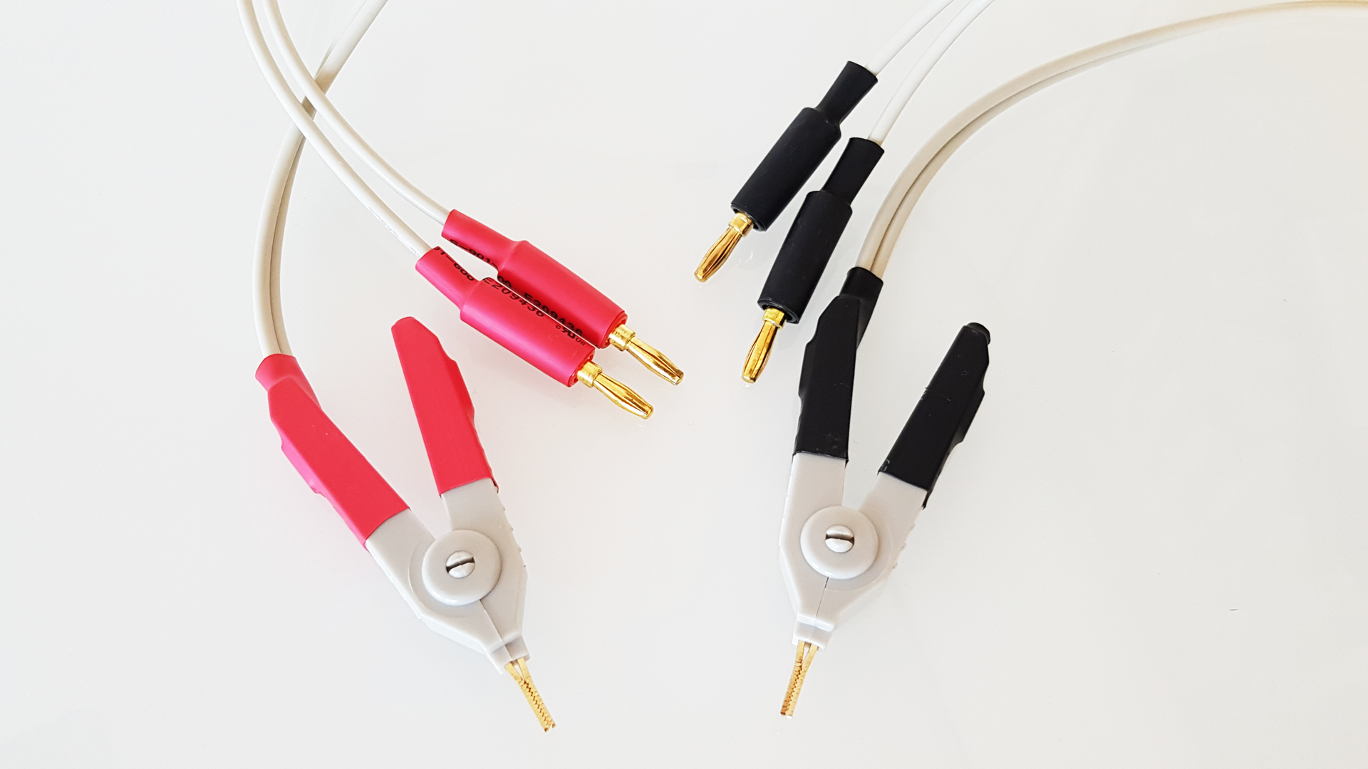
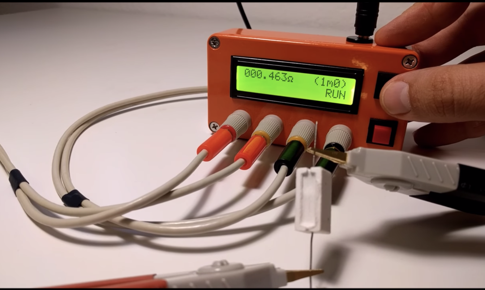
To reduce the influence of the resistance of the test leads on the measurement, the devices use Kelvin connectors as leads to connect the resistor under test to the measurement point.
Arduino based Milliohm Meter with LCD display – [Link]
The recent moves by Sonos can only be explained as targets towards expanding its connected ecosystem of smart devices and beyond. The wireless speaker company from Santa Barbara California, sometime last year acquired a French company that provides embedded assistants and interfaces for devices that run locally and offline. Of recent, the company set out to add to its league of acquisition the British data-over-sound company, Chirp.io.
Aimed at simplifying device-to-device connectivity via sound, Chirp, which was founded in 2011 at the Computer Science department of University College London, recognized the growing need for seamless low-cost, low power and frictionless communication between devices in the emerging IoT world. They pioneered a data-over-sound technology that creates simple-to-implement solutions to enhance connectivity and identification of machines. The technology helps to improve user experience and bring audio-capable devices into new possibilities thereby substantially lowering the cost for applications like proximity detection, device provisioning, and two-way acoustic NFC. They also capitalized on the digital signal processing capabilities of the Arm Cortex –M7 and Cortex-M4 to provide software-defined acoustic data transmission solutions which are quite robust and reliable, but not resource-intensive.
However, after working together with Sonos for a while now, Chirp has finally confirmed its been acquired by Sonos, describing it as “the perfect match for audio and wireless technology” since Sonos shares the same passion with them.
In an email sent to me, the chirp team mentioned that
“…Chirp has always held firm to a belief that robust, reliable data-over-sound could transform user experiences and bring new possibilities to audio-capable devices. Sonos shares this belief, alongside our common passions for engineering excellence, delightful user experience, and investment in research and development.”
The Chirp team has expressed their pleasure in seeing developers use their SDKs in a number of imaginative applications, but made it clear that starting from March 1ST, the Chirp SDK will no longer be available for users to download.
“…Having joined Sonos, access to the Chirp developer console will be closing on March 1st, meaning users will no longer be able to download Chirp SDK s after that date. If you are using an SDK that you have already downloaded for hobby or proof-of-concept work you can continue to do so freely.”
Meanwhile, these acquisitions will give Sonos a new set of talented employees to quickly bring them into a clear technology differentiation; achieving their goals without having to sacrifice their brand identity. Former CEO of Chirp and new Director of Sonos’ Emerging Technologies already confirmed that efforts with Chirp’s data-over-sound technology will now be focused on Sono’s personal Research and Development program.
F&S Elektronik Systeme GmbH presents a prototype of a direct solder module. It’a a 30 x 30mm “OSM-MX8MM” module that runs Linux on an i.MX8M Mini.
As part of the SGET, the standardization group SDT.05 was founded jointly by iesy GmbH, F&S Elektronik Systeme GmbH and Kontron AG. The aim of this group is a new standard for directly solderable modules. In the meantime, further 13 companies work on this standard.
Currently 4 sizes of 15 x 30mm, 30 x 30mm, 45 x 30mm and 45 x 45mm are planned. There will be modules from different providers in every size, also with different CPUs. A pre-release of the new standard will be available for embedded world 2020.
Features
Size-S „Small“ 30x30mm
Other sizes are planned
Open Source Standard
(not yet released)
Can be soldered on directly
(can be equipped by machine)
Scalable
Standardized interfaces
No connectors
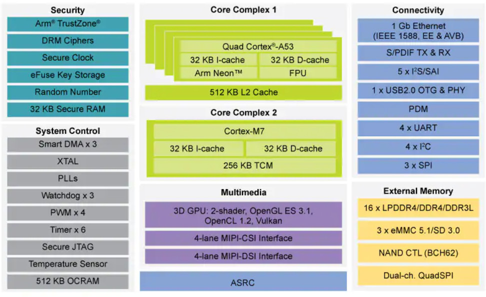
F&S Elektronik Systeme has been developing and producing embedded boards in Stuttgart for more than 20 years and offers a wide range of modules with NXP CPUs (from i.MX 6 Cortex-A7 to i.MX 8 Cortex-A53 quad-core). F&S Elektronik Systeme has developed a small (30 x 30mm) prototype so that potential customers of an OSM module not only have to look at graphic designs, but can also pick up a “real” module. A current NXP CPU, the i.MX 8 M Mini with 4x Cortex-A53 @ 1.8GHz, was selected. A powerful CPU with a lot of computing power and 2D / 3D graphics unit and video decoder. The pin-compatible i.MX 8 M Nano CPU can alternatively be equipped. RAM, flash on board and interfaces such as LAN, USB, SDIO, UART, I2C, SPI, audio, GPIO, MIPI-CSI and MIPI-DSI are available.
No pricing or availability information was provided for the OSM-MX8MM module. More information may be found in F&S Elektronik Systeme’s announcement and preliminary product page. Interested visitors can see the module at the F&S Elektronik Systeme booth at embedded world 2020 (Hall 2-138) and ask questions.
One of the best things about being a maker is the ability to make your own tools. We have covered the development of several electronics tools in past, from voltmeters to battery testers. For today’s tutorial, we will add another tool to the list by examining the development of a Miliohm meter made by danielrp @ www.instructables.com
A milliohm meter is a device used in determining the resistance of small resistors, PCB traces, motor coils, inductance coils, and transformer coils, or calculate things like the length of wires. It provides a resolution, not built into regular multimeters, making it easy to get accurate readings in the milliohm range.
There are quite a number of Miliohmeter builds on the internet, but today’s tutorial will chronicle the efforts of instructable user Danielrp. Daniel’s version of the meter is based on a precision current sink and a high-resolution ADC controlled by an Arduino Nano. The current sink is based on the LT3092 precision current source/sink which, using a network of resistors and transistors is set to function as a sink. For the ADC, the high resolution, MCP3422A0 I2C ADC is used. Just one of the channels of the ADC is used, and it is connected differentially to the Resistor under test “S+ S-“. The MCP3422 is configured as 18bit but as S+ is always going to be greater than S-, the effective resolution is 17bit.
To reduce the influence of the resistance of the test leads on the measurement, the devices use Kelvin connectors as leads to connect the resistor under test to the measurement point.
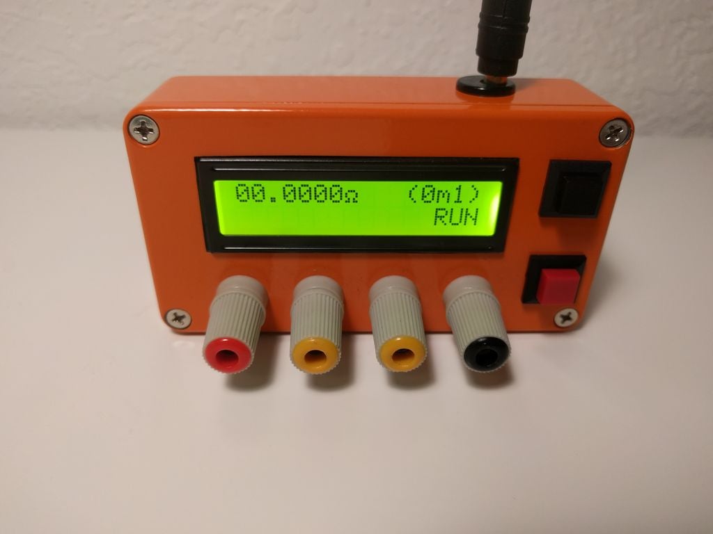
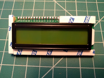
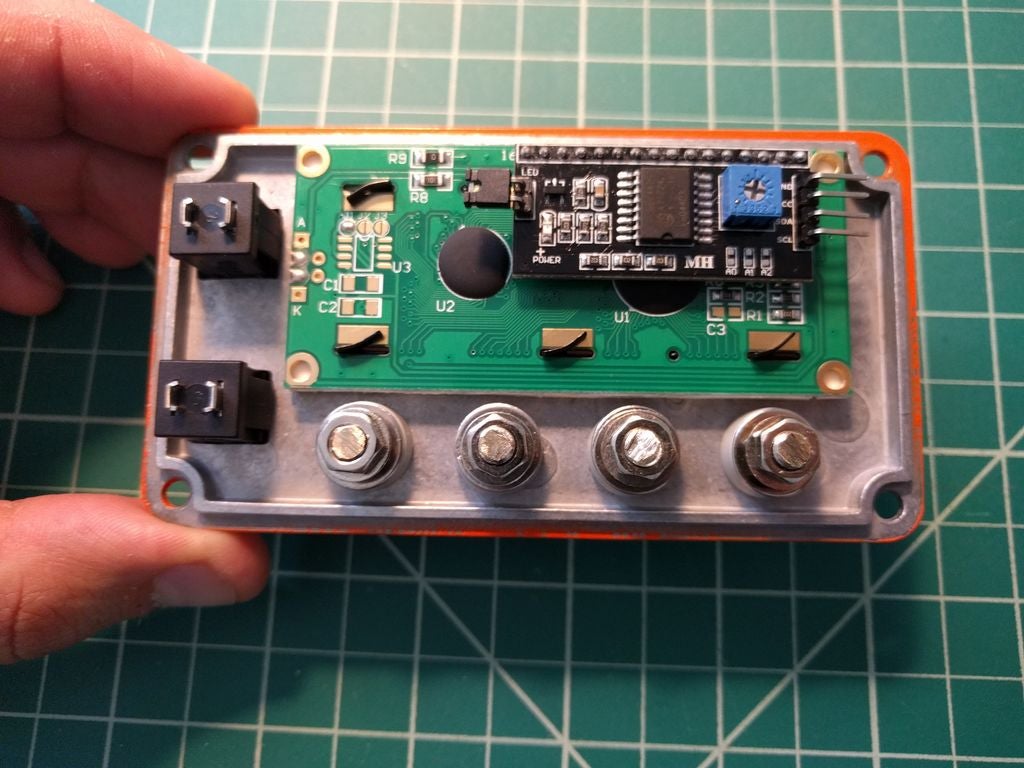
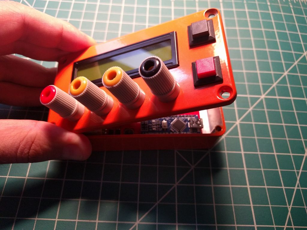
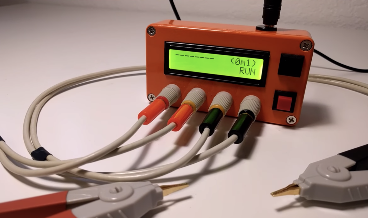
Users can make the selection between the above measurement ranges by using one of the two push buttons on the device. Visual feedback on the selections and meter readings is provided to users via a 16×2 LCD display, and the entire project is enclosed in an orange Hammond 1590B aluminum box to make it handy and presentable.
Ready to build? let’s dive in.
Required Components
Due to the bulkiness, the complete list of components required to build the project is attached under the download section. However, some of the key components to be used include:
Arduino Nano
16×2 LCD Display
ULN2003A
LT3092EST
MCP3422A0
Kelvin Connectors
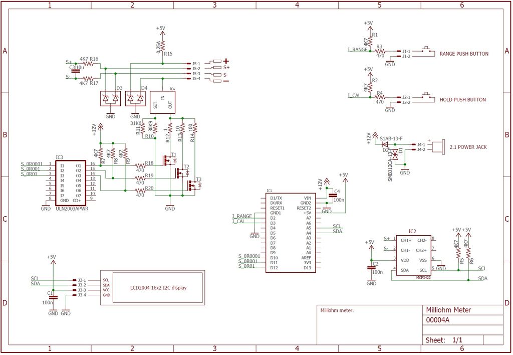
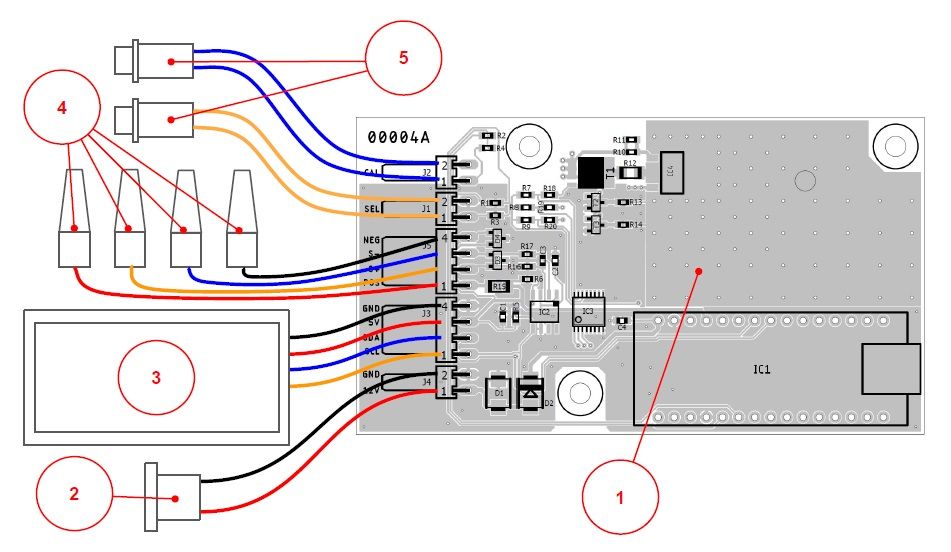
Schematics
Due to the complex nature of the project, implementing on a breadboard will not only be time-consuming but also make the project susceptible to errors. To prevent this, the project was implemented on a PCB designed with Eagle. The schematics showing how the components are connected on the PCB is provided below:
Both the schematics and PCB files are attached to the BOM under the download section. It should make modifying the project for your personal use a bit easier.
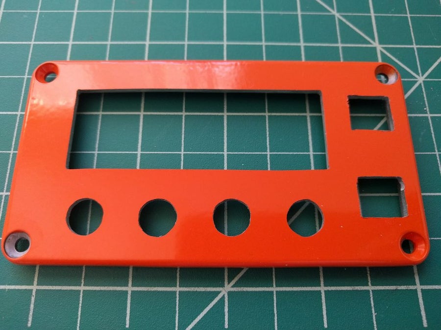
Enclosure and Assembly
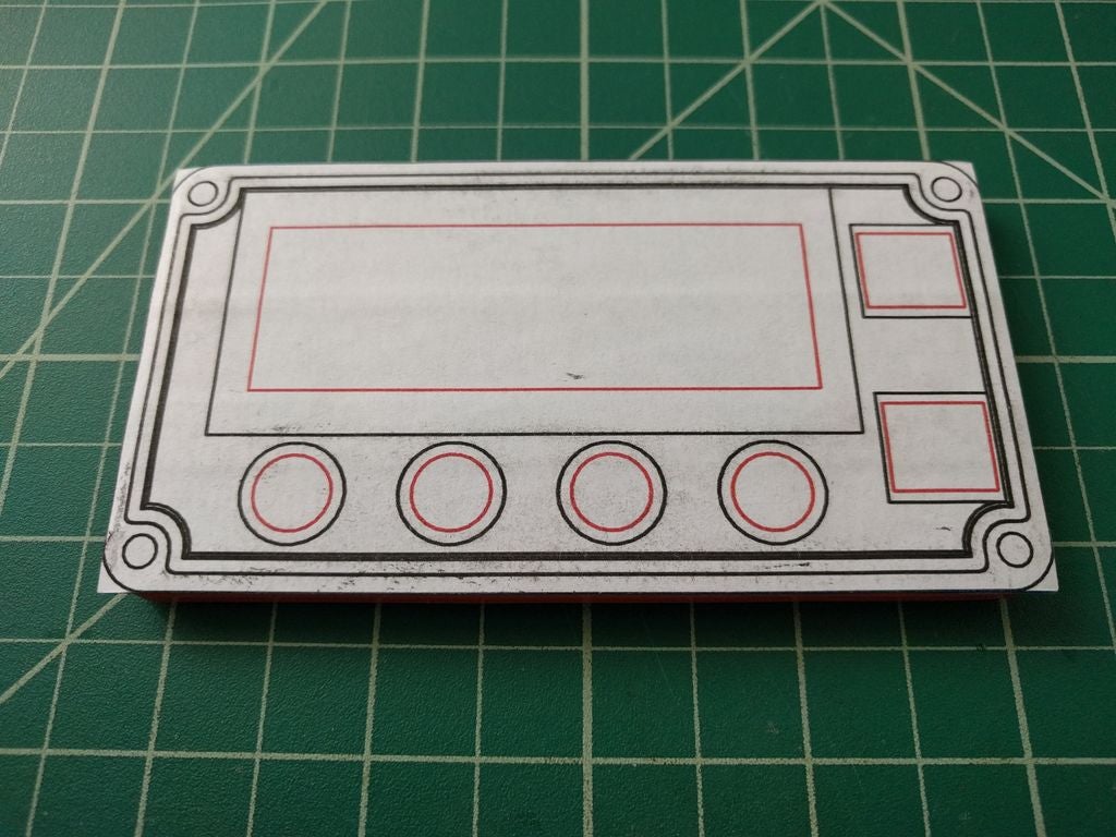
The PCB approach was adopted to make the project presentable and useful and to take things even further, DanielrP developed an enclosure for the project.
The modification to the Aluminium enclosure box was designed with Inkscape and the design files, along with the stencil are attached under the download section.
7. With all the components installed, the top/cover should look like the image below.
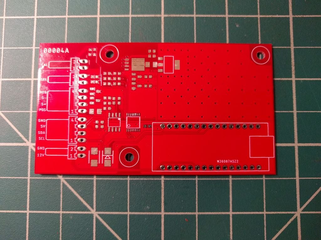
Before coupling together the enclosure, it might be smart to first get some components of the PCB in place. Since most of the components used for the PCB are SMT types, mounting them on the PCB will require the use of a hot-air gun or the use of a regular soldering iron along with a fine-tip tweezer, some solder wick, and a 0.02″ solder.
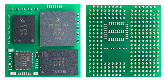
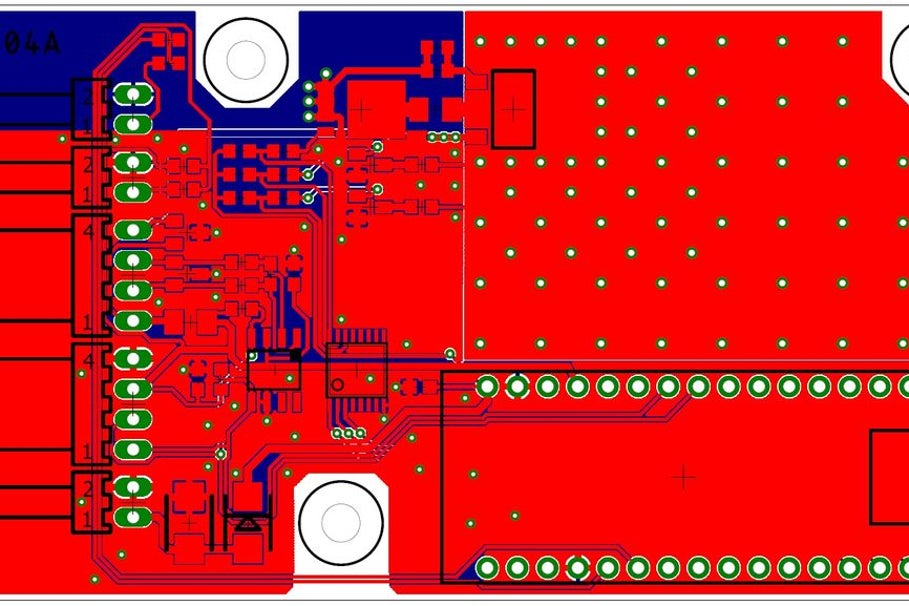
The image below provides a broad overview of where some of the components go on the PCB.
Since the kelvin connectors and switches are only useful on the outside of the enclosure, they will be connected to the PCB via jumper wires as shown above.
With the PCB and the box now ready, install the PCB in the box and connect the pushbuttons and kelvin connectors.
To make it easy to upload code to the setup when completed, you can open a small hole close to the USB port on the Nano, so a USB cord can be easily connected to it.
With this complete, we are now ready to write the code for the project.
Code
The algorithm behind the code for the project is quite complex. We set the scale for the project by driving the set pins connected to the ULN2003. The scale along with the mode (which is determined by the status of the pushbuttons), is then taken into account and the MCP3422 is read to obtain the resistance value and display it on the LCD.
Since the sketch is already a complex one, to reduce the complexity a bit, a number of libraries were used, including; the Wire.h library, the LiquidCrystal_I2C library, and the EEPROM library. The wire library was used to facilitate I2C Communication between the Arduino and the two I2C components of the project; the LCD and the MCP3422. The LiquidCrystal_I2C library, on the other hand, helped with interfacing with the LCD, while the EEPROM Library was used in accessing the EEPROM on the Arduino to store information about the mode and meter scale.
The Wire and EEPROM libraries come preloaded with the Arduino IDE, while the LiquidCrystal_I2C library can either be installed via the link attached to it or by installing it via the Arduino Library Manager.
As usual, I will do a quick run down and explain some snippets/parts of the Sketch. The code is quite bulky and might be difficult to cover all of it but luckily, Daniel did a good job with comments on each line of code so it should be easy to follow it.
We start the sketch by including all the libraries we will be using.
Next, we specify the dimensions of the display and create macros for the scale. This basically sets the status of pins involved with setting the scale.
Next, create macros for the Arduino built-in led, which will be used to provide visual feedback as regards the status.
We follow this with a configuration of the pushbuttons. One to turn it on or off and the other to take it in and out of calibration mode.
Next, we declare some of the variables that we will be using for the MCP3422 related data. We specify variables to hold the channels, the slave address and other things.
//MCP3422
#define MCP3422_CH1 0x00
#define MCP3422_CH2 0x01
#define MCP3422_SR 0x03 //3.75 SPS (18bit)
#define MCP3422_GAIN 0x00 //x1
#define MCP3422_CR_STARTONESHOT 0x80 // /RDY bit = 1, /O/C bit = 0
#define MCP3422_CR_READY 0x80        // /RDY bit mask
#define MCP3422_NCH 2u    //Number of channels available
#define MCP3422_ADD 0x68  //Slave address
Next, we create a string of messages that will be displayed.
Next, we call the setupDisplay() function to initialize the LCD and display a sort of splash screen.
setupDisplay();
The above is followed by setting the speed of I2C communication, turning the backlight of the LCD high, and rounding up the setup function by initializing Serial communication so the serial monitor can be used for debugging purposes.
  Wire.setClock(400000);  //Speed for both display and MCP3422
  lcd.setBacklight(HIGH);
  Serial.begin(9600);


}
Up next is the void loop() function. The function starts with a line of code to obtain an update on the status of the pushbuttons, the modes and scale among others.
This is followed by an if statement which checks if the device is in hold mode. If the device is in hold mode, the scale and the measurement are obtained but if it’s not(run mode), Update bufferA with the “RUN” text, Read the RUN scale, Set the RUN scale in the current sink, check if data is available from the MCP3422, and start a new data conversion on the channel.
if(true == eeIsHoldMode())
  {//Hold Mode
    writeString(1u, 12u, strHOLD);                    //Update bufferA with the "HOLD" text
    eeReadU8(EE_U8SCALEHOLD, u8CurrentScale);         //Read the HOLD scale
    eeReadU32(EE_U32MEASHOLD, u32CurrentMeasurement); //Read the HOLD measurement
  }
  else
  {//Run Mode
    writeString(1u, 12u, strRUN);                     //Update bufferA with the "RUN" text
    eeReadU8(EE_U8SCALERUN, u8CurrentScale);          //Read the RUN scale
    changeScale(u8CurrentScale);                      //Set the RUN scale in the current sink
    //Read the ADC if a new measurement is available.
    if(MCP3422_IsDataAndRead(u32CurrentMeasurement, bMCP3422ValIsPositive))
    {//New conversion available
      if(false == bMCP3422ValIsPositive)
      {
        u32CurrentMeasurement = 0;
      }
      MCP3422_StartConversion(MCP3422_CH1);   //Restart conversion
    }
  }
Finally, the display buffer is updated, and the value is displayed on the LCD using the updateDisplay() function which wraps up the loop().
  updateDisplayBuffer();                              //Update the rest of BufferA
  updateDisplay();                                    //Write the necessary chars in the display
}
The void loop() and void setup() discussed above contain very few lines of code because the majority of the work is done in several other functions. From the function which handles data conversion on the MCP3422 ADC to the one used in setting the scale and the one used in updating the display, all of this function play an important role and while its a bit difficult to go over them one after the other because of how bulky it will make the tutorial, the code to implement them is properly commented by Danielrp so it should be easy to follow.
The complete sketch is attached in the zip file under the download section below.
Demo
With the code complete and the hardware in place, connect the device to your computer and upload the code to it.
After a while, you should see the display come up as shown in the image below.
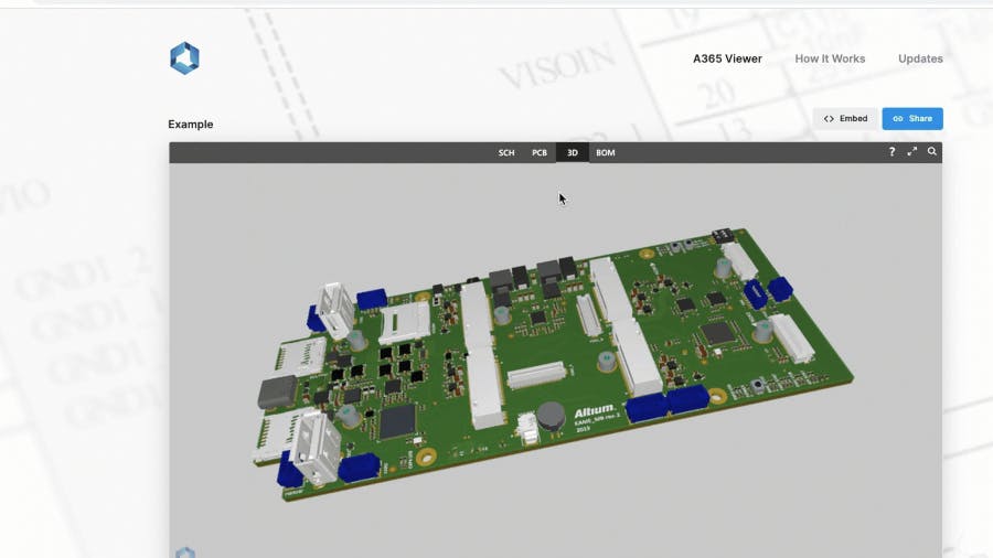
Altium has launched a new, cloud-based application – the A365 Viewer – that redefines the way that printed circuit board designs are shared between designers, part suppliers, and manufacturers.
“Adding the Altium 365 Viewer has significantly enhanced the user experience when navigating the product documentation on our website. Now Arduino users can freely browse schematics, PCB layout and even 3D models of the Arduino boards and modules online, without the need to download or install anything additional. The capability of being CAD-agnostic will shorty allow Arduino to add the online design viewer to every product page, including the ones designed in Autodesk Eagle.” – Fabio Violante, CEO, Arduino
Altium, a global leader in PCB design software, announced the launch of a new cloud-based application that redefines the way that printed circuit board designs are shared between designers, part suppliers, and manufacturers.
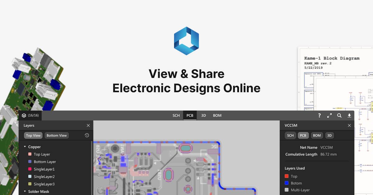
The A365 Viewer, powered by the Altium 365 cloud platform, is a brand new, and innovative way to view and share electronic designs through a browser on any web-enabled desktop, phone or tablet. Schematics, PCB layout, and 3D visualization provide an interactive eCAD experience with no downloads or installations required. The A365 Viewer is part of Altium’s cloud strategy and newly launched Altium 365 cloud platform.
Simplicity is the Ultimate Sophistication
Until now, designers have been forced to share their PCB designs through PDFs or static images. With the new A365 Viewer, an interactive experience is created that retains all of the key relevant information that’s typically lost when sharing static files. For example, the A365 Viewer allows users to search for, select, cross-probe and inspect components and nets while moving seamlessly between schematic, PCB and 3D views of their board.
Using the A365 Viewer requires no CAD tools or experience. The A365 Viewer is designed to work with multiple eCAD formats, currently supporting Autodesk®️ Eagle™ and Altium Designer™. Other popular PCB design software formats will be supported in the near future.
Visually stunning, interactive CAD centric renditions of user PCBs, including Schematic, PCB, 3D and BOM all easily available through a browser on any web-enabled device.
Easily Embedded on Your Website
Anyone can easily embed the viewer on their website, free of charge, by visiting www.altium.com/viewer/. As an example, a well-known developer of electronics hardware and software kits, Arduino, is helping engineers and makers to easily and quickly visualize the PCB designs and assemblies available in their product kits, by embedding the A365 Viewer on the Arduino website.
Built-in Design IP Protection
The A365 Viewer protects the IP rights of design owners while retaining the CAD design details via a new process called Published Design Impression (PDI). The Viewer processes the design source files to create a Published Design Impression, or PDI. The PDI is a CAD-aware, perishable snapshot of the design that captures limited information such as components, net connectivity and basic geometrics, excluding design primitive data that would be required to fully comprehend and author changes to the design.
The design sources are discarded immediately after being used solely for the purpose of creating a PDI. The design is available for the duration of the user’s browser session and is automatically removed when the browser tab is closed.
We embedded it in Electronics Lab
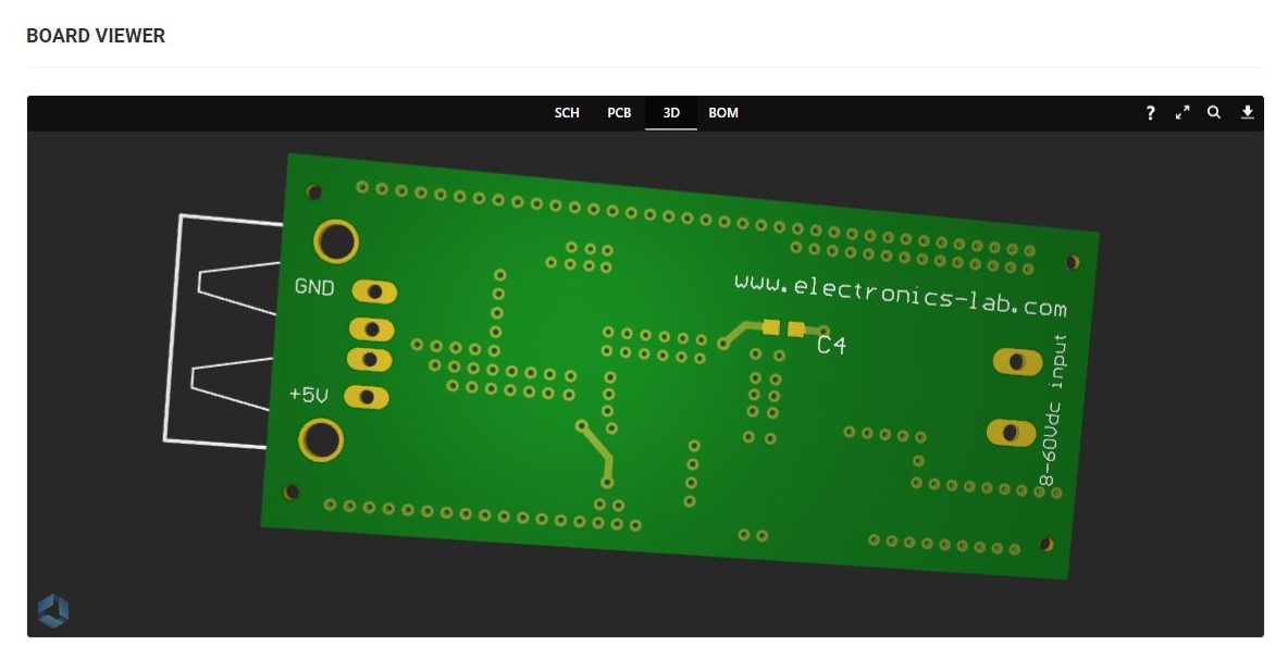
We have embedded the viewer on a project here on electronics-lab.com to test it out. You can check the A365 Viewer on 60V to 5V @ 3.5A Buck converter with USB output near the bottom of the page. It seems a great tool, to view Schematic, PCB, 3D View and BOM of any project on Eagle and Altium. More CAD tools support is on the way. Share your opinion on the comments!
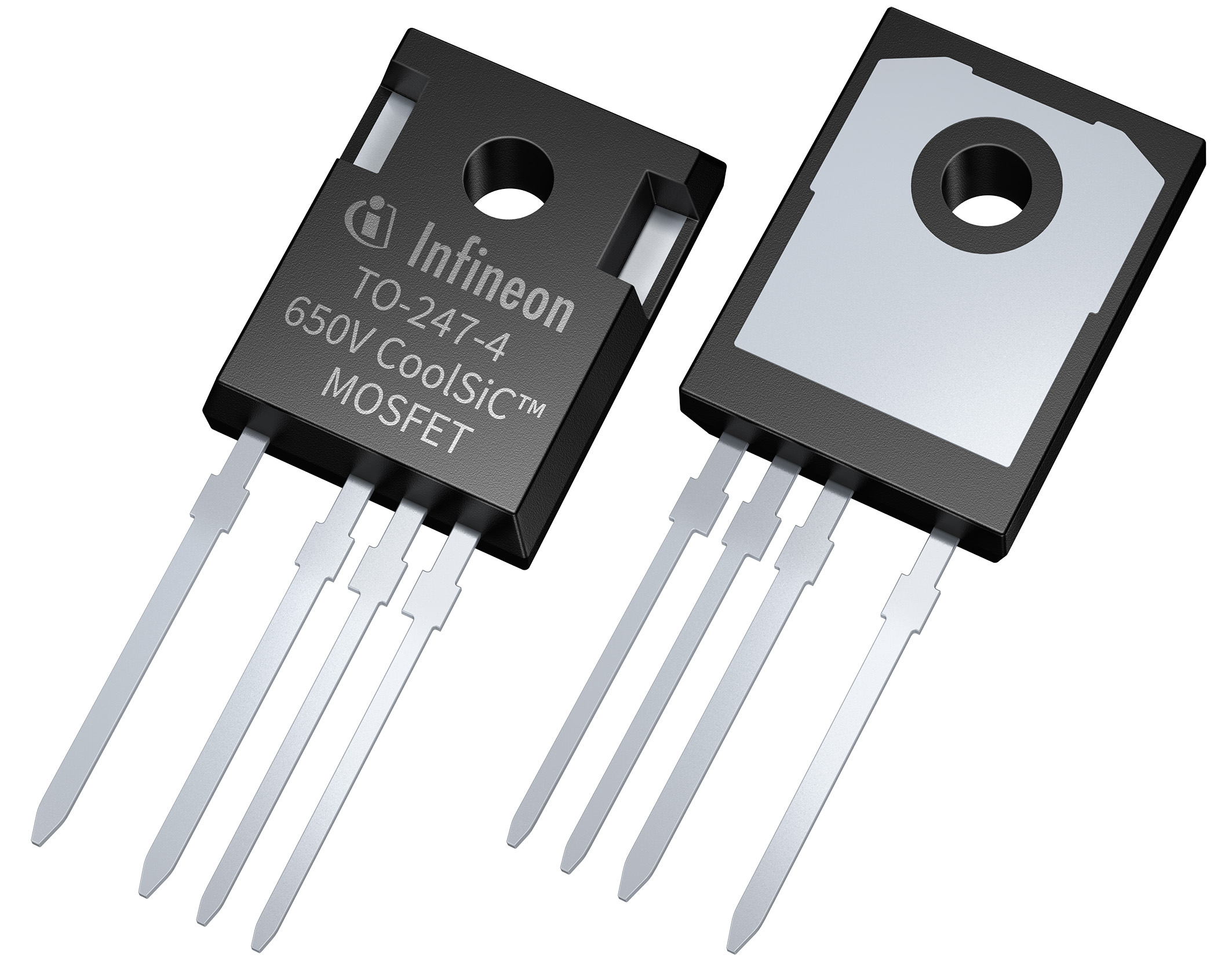
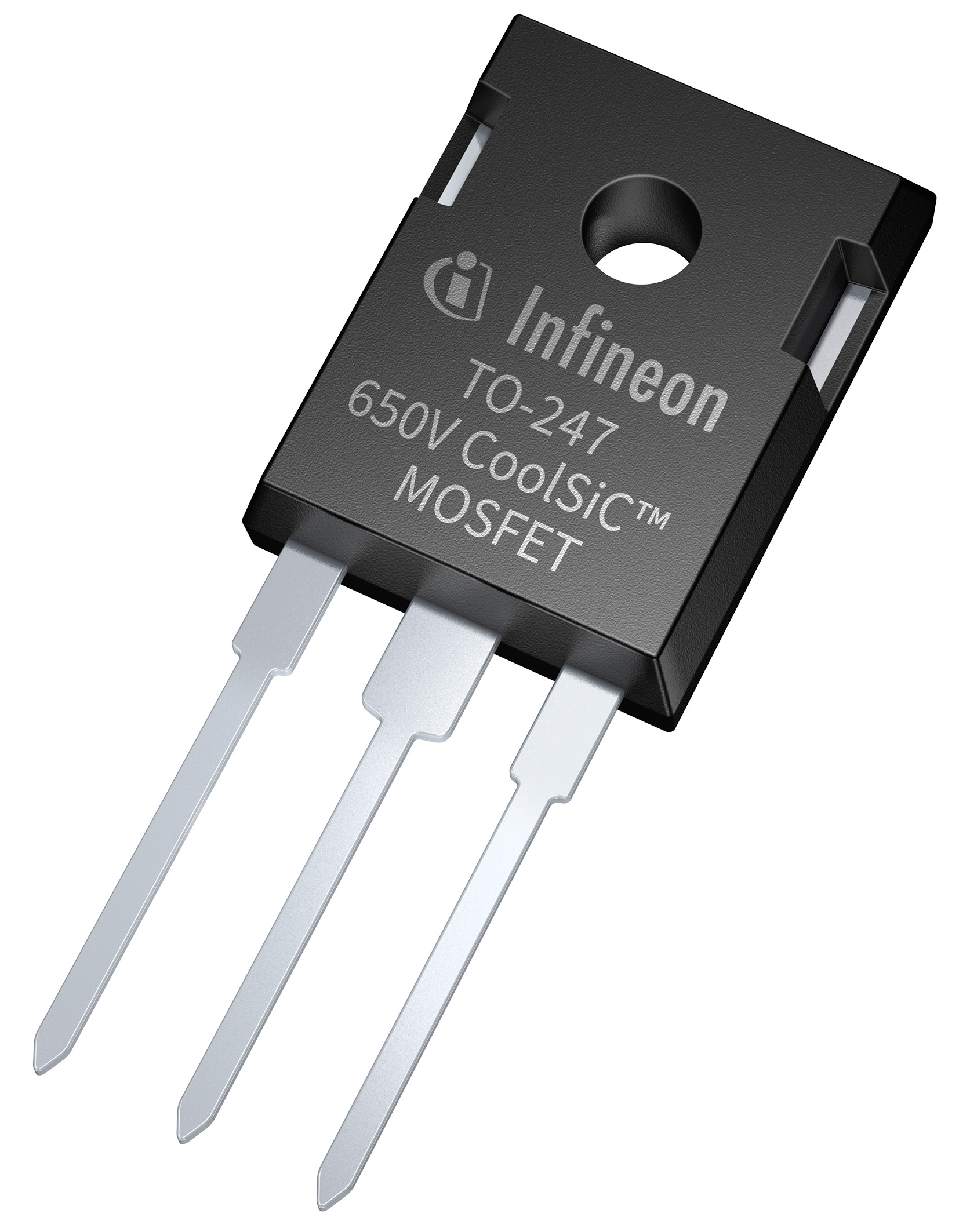
Infineon Technologies AG continues to expand its comprehensive silicon carbide (SiC) product portfolio with 650 V devices. With the newly launched CoolSiC™ MOSFETs Infineon is addressing the growing demand for energy efficiency, power density, and robustness in a wide range of applications. Amongst them are server, telecom and industrial SMPS, solar energy systems, energy storage and battery formation, UPS, motor drives as well as EV-charging.
“With this launch, Infineon complements its broad silicon, silicon carbide, and gallium nitride-based power semiconductor portfolio in the 600 V / 650 V power domain,” said Steffen Metzger, Senior Director High Voltage Conversion at Infineon’s Power Management & Multimarket Division. “It underlines our unique position in the market being the only manufacturer with such a broad offering for all three power technologies. Additionally, the new CoolSiC family supports our claim to be the number 1 supplier of SiC MOSFET switches for industrial purposes.”
The CoolSiC MOSFET 650 V devices are rated from 27 mΩ to 107 mΩ. They are available in classic TO-247 3-pin as well as TO-247 4-pin packages, which allows for even lower switching losses. As for all previously launched CoolSiC MOSFET products, the new family of 650 V devices are based on Infineon’s state-of-the-art trench semiconductor technology. Maximizing the strong physical characteristics of SiC, this ensures that the devices offer superior reliability, best-in-class switching and conduction losses. Additionally, they feature highest transconductance level (gain), threshold voltage (V th) of 4 V and short-circuit robustness. Thus, trench technology allows for the lowest losses in the application and highest reliability in operation – without any compromise.
650 V CoolSiC MOSFETs offer attractive benefits in comparison to other silicon and silicon carbide solutions in the market such as switching efficiency at higher frequencies and outstanding reliability. Thanks to the very low on-state resistance (R DS(on)) dependency on temperature they feature an excellent thermal behavior. The devices boast robust and stable body diodes retaining a very low level of reverse recovery charge (Q rr), roughly 80 percent less compared to the best superjunction CoolMOS™ MOSFET. The commutation-robustness helps in achieving very easily an overall system efficiency of 98 percent, e.g. through the usage of continuous conduction mode totem-pole power factor correction (PFC).
To ease the application design using CoolSiC MOSFETs 650 V and to ensure high performance operation of the devices, Infineon offers dedicated 1-channel and 2-channel galvanically isolated EiceDRIVER™ gate-driver ICs. This solution – combining CoolSiC switches and dedicated gate-driver ICs – helps lowering system costs as well as total cost of ownership and enables energy efficiency gains. The CoolSiC MOSFETs also work seamlessly with other ICs from Infineon’s EiceDRIVER gate-driver family.
Availability
The CoolSiC MOSFET 650 V family comprises eight variants housed in two through hole TO-247 packages. They can be ordered now. Three dedicated gate-driver ICs will be available starting March 2020. More information is available at www.infineon.com/coolsic-mosfet-discretes.
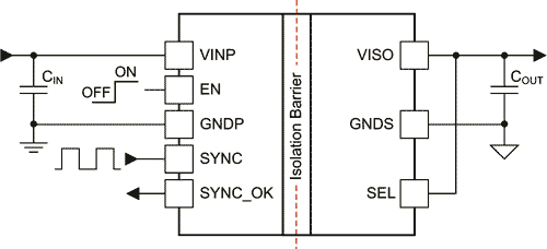
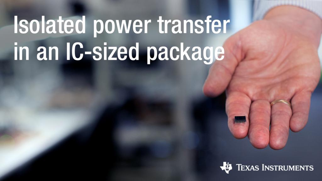
Engineers can shrink their power solution by as much as 80% and maximize efficiency in high-voltage industrial applications with a new high-density, isolated DC/DC bias power supply.
Texas Instruments (TI) introduced the first integrated circuit (IC) developed with a new proprietary integrated transformer technology: a 500-mW high-efficiency isolated DC/DC converter with the industry’s lowest electromagnetic interference (EMI), the UCC12050. Its 2.65-mm height enables designers to reduce their solution volume by as much as 80% compared to discrete solutions and 60% compared to power modules – with twice the efficiency of competing devices. Built for industrial performance, the UCC12050’s 5-kVrms reinforced isolation and 1.2-kVrms working voltage protect against high-voltage spikes in systems such as industrial transport, grid infrastructure and medical equipment.
Simplified Application Schematic.
TI’s breakthrough integrated transformer technology enables high-density isolated DC/DC power conversion, while maintaining low EMI. The single-package, surface-mount architecture gives designers an easy-to-use, low-profile IC that reduces the bill of materials (BOM), and efficiently operates across a wide temperature range. An EMI-optimized, low capacitance transformer and quiet control scheme streamline EMI compliance while providing a reliable solution with options for reinforced or basic isolation.
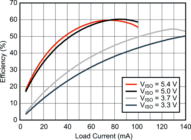
Typical Efficiency vs. Load @ VINP = 5.0 V.
Key features and benefits of the UCC12050
Small size, increased power density:
Available in a 16-pin small-outline integrated circuit (SOIC) package measuring 10.3 mm by 10.3 mm by 2.65 mm, the UCC12050 offers 60% efficiency – twice that of competing devices of similar size – and twice the power density of comparative isolated power modules. Delivering 0.5 W in the new architecture improves reliability, enables a small BOM and simplifies board layout.
Ultra-low EMI:
The UCC12050’s integrated transformer with very low primary-to-secondary capacitance is optimized for EMI performance, and its quiet control scheme makes it easier for engineers to have their designs pass Comité International Spécial des Perturbations Radioélectriques (CISPR) 32 Class B EMI tests, with margin, on a two-layer printed circuit board. The solution also eliminates external filter components such as low-dropout regulators and ferrite beads normally required to meet EMI certification, which significantly reduces component selection and design time.
Reinforced isolation, wide temperature range:
The UCC12050’s reinforced isolation with 8-mm creepage and clearance is used for protection and robustness against ground potential differences. Its high efficiency and extended –40 °C to 125 °C operating temperature range deliver more power in extreme conditions.
This new high-density isolated power converter, the latest industry-leading device in TI’s power-management portfolio, offers small size and ease of use for any industrial application requiring isolation. Additionally, the new UCC12040 provides all of the same benefits with 3-kVrms basic isolation.
Package, availability and pricing
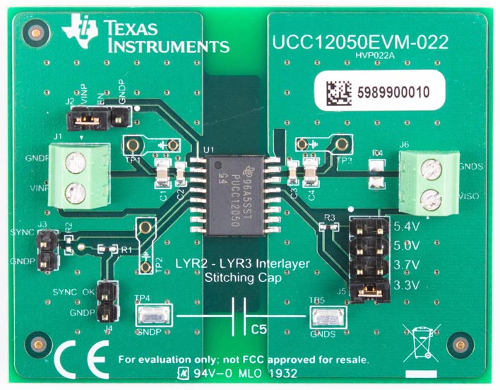
The UCC12050 and UCC12040 are available in volume production from TI and authorized distributors in a 16-pin, 10.3-mm-by-10.3-mm-by-2.65-mm SOIC package. Pricing starts at US$3.90 and US$3.15, respectively, in 1,000-unit quantities. Engineers can evaluate this product with the UCC12050EVM-022 evaluation module, available on TI.com for US$99.
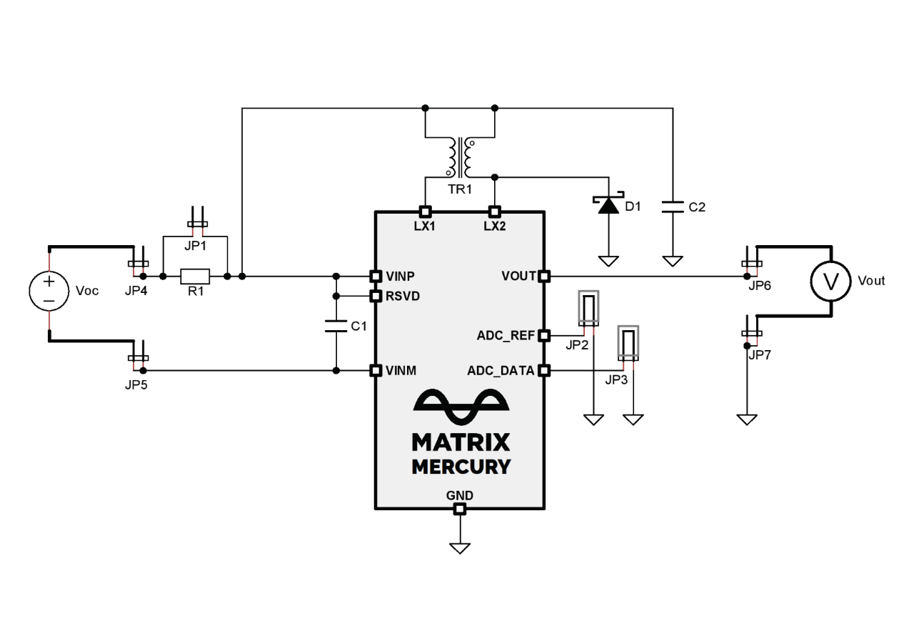
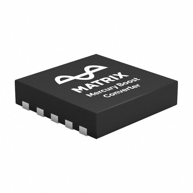
MATRIX Industries’ nanopower energy harvesting boost converter with microwatt cold-start, input impedance matching, and regulated output
MATRIX Industries’ Mercury is a family of highly integrated DC/DC boost converters that are ideal for harvesting and managing surplus energy from extremely low input voltage sources such as TEGs (thermoelectric generators) and thermopiles. The patented transformer reuse topology works as a flyback converter and can operate from input power of as little as a few microwatts. The unique impedance matching feature presents a constant impedance load and enables the highest efficiency energy harvesting across the entire operating range of input voltages.
Features
VIN as low as 10 mV (VOC=20 mV, RIN=5 Ω) to VOUT of up to 5 V
VIN as low as 6 mV (VOC=12 mV, RIN=5 Ω) to VOUT of 3 V
Ultra-low quiescent current of 700 nA ensures the fastest possible charge times of the output reservoir capacitor
Cold-start with VOC=16 mV (RIN=5 Ω, 1:100 transformer)
Up to 80% peak conversion efficiency
Near-ideal impedance matching with input source
Built-in VOC monitoring through an 8-bit ADC
True shutdown by disconnecting output when VOC is below startup requirement securing zero power leakage
Three external components are required: input capacitor, output capacitor, and transformer
Optional Schottky diode for efficiency improvement
Compact WLP package available
There are multiple input protection voltage options available based on the ratio of the transformer. The 8-bit on-chip ADC detects when VOC exceeds the programmed limit and turns off the input to ensure reliable operation. The result of the measurement is transmitted via a two-wire interface to a microcontroller. The converter is available in maximum output voltages from 2 V to 5 V. Integrated VOUT regulation prevents voltage overshoot, securing reliable operation with various battery types.
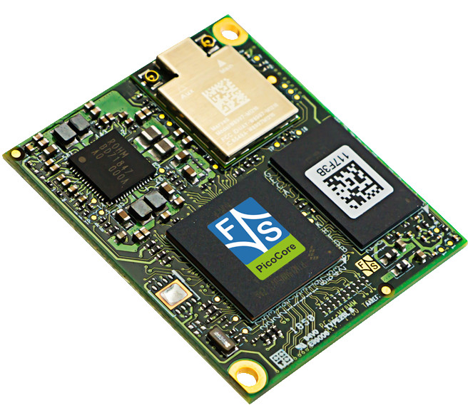
COM modules with NXP i.MX 8M Nano CPU High performance in a compact format
Based on the NXP® i.MX 8M Nano applications processor, F&S Elektronik Systeme has developed an inexpensive CPU module (35x40mm) with many industrial interfaces and extensive software support.
The heterogeneous multi-core processor consists of up to four Arm® Cortex®-A53 cores (1.5GHz) and an additional Cortex®-M7 for real-time processing. Up to 2x Gbit Ethernet, CAN-FD, USB, 2x SDIO, 4x I2C, 2x SPI, 4x UART, audio (Line In/ Out/ Mic/ Headphone or I2S), GPIOs, PWM and MIPI-CSI for camera connection are available. Displays can be connected either via a MIPI-DSI interface (4 lanes) or via LVDS (2 channels). The maximum resolution is FullHD. The optional WLAN/ BT5.0 LE module with antenna socket also makes portable applications possible.
The i.MX 8M Nano is equipped with OpenGL 2.1/ 3.0/ 3.1 and OpenCL 1.2, providing sufficient performance for a modern user interface.
The PicoCore™MX8MN is offered with up to 8GB RAM, 512MB SLC NAND Flash or 32GB eMMC. A small NOR Flash for storing device parameters is of course also provided.
Besides Secure Boot (protection of the system against manipulation and protection of the software against decryption), an additional security chip (NXP A71CH Plug-&-Trust-Secure-Element) offers further security for IoT connections. The programming of the certificates can be done by the customer himself, alternatively F&S Elektronik Systeme offers this as a service.
The operating system Linux® (with support for Buildroot and Yocto), was ported by the experienced software team of F&S Elektronik Systeme. For all interfaces the drivers have been adapted and tested. Different memory sizes and different displays are supported. For many touch controllers there are ready-to-use drivers. For the Cortex®-M7 an adapted FreeRTOS and various “Bare Metal” examples are available. The communication between Cortex®-M7 and Cortex®-A53 is implemented and tested. The Cortex®-M7 is able to process real-time tasks shortly after power-on.
Extensive documents explain the development on Linux side as well as on Cortex®-M7 side. With the help of the virtual machine provided for download, the development of the own application, e.g. under QT, can be started immediately.
The PicoCore™ standard (35×40 mm) uses two connectors (Hirose DF40C) with 100 pins each. This allows a compact design and a small board-to-board distance (1.5-4mm board) and is available in 0°C – 70°C but also down to -40°C – +85°C.
With the F&S project guarantee, F&S Elektronik Systeme accompanies the customer from the start of the project to the successful completion of the project. Starterkit (including 7″ touch display), workshops, documents for hardware and software development and free support by the experienced engineers of F&S Elektronik Systeme GmbH are available for this purpose.
The PicoCore™MX8MN is available at least until 2029 and in the meantime six PicoCore™ COM modules with NXP CPUs are available, more will follow.