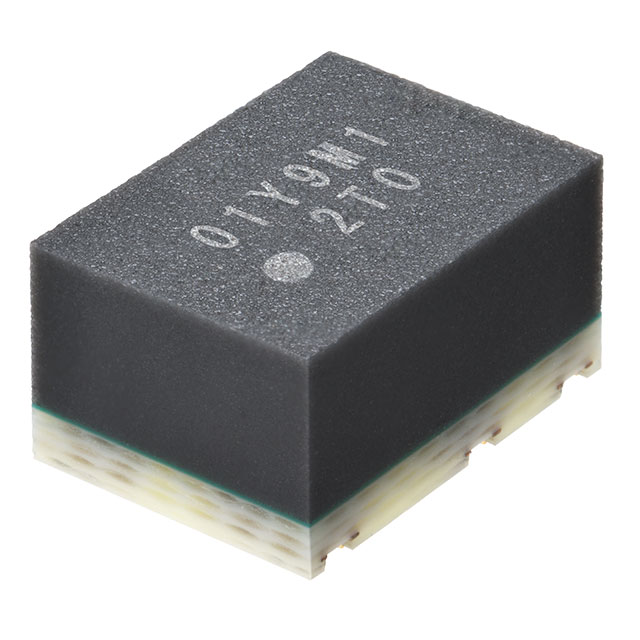
OMRON Corporation of Kyoto, western Japan globally released its new MOS FET (*1) relay module “G3VM-21MT” on December 2, 2019.
The product is the first electronic component in the world (2) to adopt a “T-type circuit structure” (3). With a T-type circuit structure consisting of compact-size and longer-lifecycle solid-state relays that output signals using no physical contact, the relay module minimizes the leakage current (*4) that has long been a problem with semiconductor test equipment. G3VM-21MT allows high-precision measurement and improves the productivity of electronic components.
Features
Contribute to reduce the mounting space on the print circuit board by small package
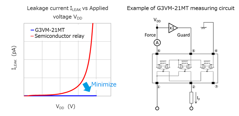
Current leakage when the main line is open and sub line is close :1 pA (Maximum) at VOFF =20 V
Contact form: 1a (SPST-NO) + T-switch function
Surface-mounting
G3VM-21MT enables switching measurement signals in test equipment mainly used to perform electrical tests for semiconductor devices. In addition to the MOS FET relay features of compact size and longer lifecycle, G3VM-21MT is the world’s first MOS FET relay module with “T-type circuit structure” which consists of three MOS FET relays that help reduce the leakage current to a minimal level without affecting test equipment’s inspection accuracy while allowing high-precision measurement and decreasing maintenance frequency of test equipment.
Amid the digital age where functions of electronic components are getting diversified and production volume is increasing, there is a growing need for higher performance of semiconductor test equipment. Mechanical reed relays (*5), which have been used for a part that performs a high-precision measurement in semiconductor test equipment, have extremely low leakage current but they require replacement on a regular basis, maybe several times for every single month due to wear and abrasion of the contacts that lead to affecting measurement accuracy. Such maintenance work may substantially affect production efficiency and so the adoption of solid-state relays has been long desired for their longer lifecycle. So far, MOS FET relays are considered not suitable for precise electrical tests due to technical difficulty to reduce leakage current in relation to its feature and were not used in test equipment which requires high reliability.
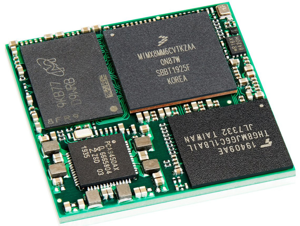
Kontron, a leading global provider of IoT/Embedded Computing Technology (ECT), will present its new System-on-Module (SoM) based on the latest processor and memory technology at the Embedded World trade fair in Nuremberg. The new SoM SL i.MX8M Mini provides an excellent and cost-effective basis for individual board and application developments.
The new SoM SL i.MX8M Mini is based on the latest processor technology 4x Arm® Cortex®-A53, 1x Arm® Cortex®-M4 and the memory technology LPDDR4. The compact module stands for maximum simplicity and efficiency within the smallest space (30 mm x 30 mm). It offers the highest performance for computing-intensive applications, demanding 3D visualizations and is optimally equipped with extensive interfaces. The ready2use Linux Board Support Package (BSP) is immediately and easily deployable for IoT and Industry 4.0 applications. Thanks to its compact design, the SoM module is predestined for a wide range of baseboard designs. Kontron also provides a corresponding evaluation board (form factor: 4.3″ diagonal) as a reference design. Since it is a machine-solderable module, there are no costs for the connectors on the SoM module and on the baseboard, nor for manual assembly.
To meet even the highest security requirements, the SoM SL i.MX8M Mini can be equipped with the latest encryption techniques, secure boot, and other security features. In combination with current wireless technologies and modern software architectures, it is a perfect building block for the development of secure devices in large IoT networks.
The Kontron System-on-Module is equipped with 1GB LPDDR4 RAM (optionally up to 4 GB), 2 MB NOR Flash and 8 GB eMMC (optionally up to 164 GB) as a standard. The SoM has 1x 1 Gbit/s (MAC), 2x USB 2.0 OTG and 4x UART ports. Numerous digital I/Os, as well as PWM and two SDIO interfaces, make the SoM module perfectly suited for industrial applications. 1x MIPI DSI is available for connecting a display and 1x MIPI CSI2 for connecting a camera. Power is supplied via a 5V DC connection. The application range lies between -25°C and +85°C.
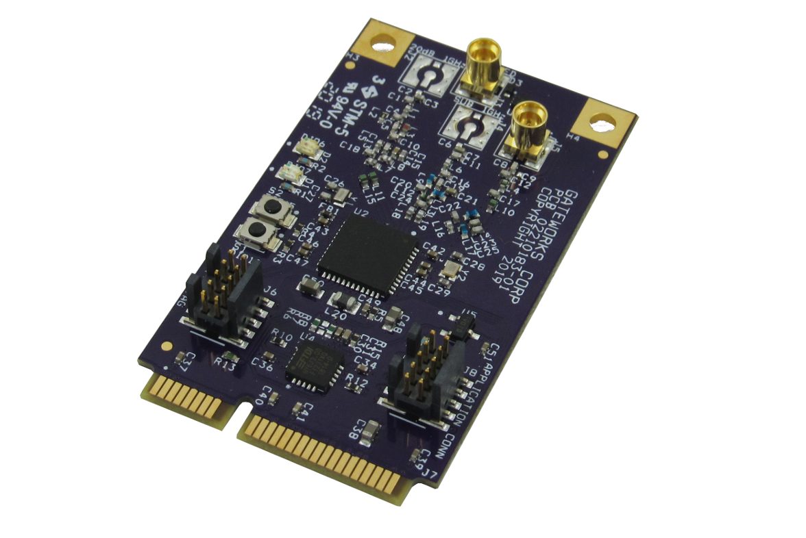
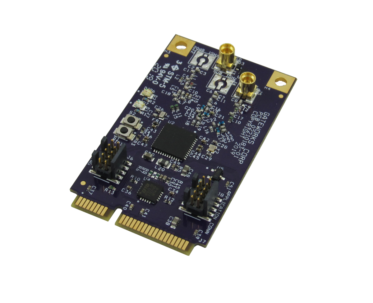
The Internet of Things (IoT) is rapidly being adopted by nearly every industry in the world to allow control and monitoring of almost anything! Gateworks has released the second generation of the GW16122 IoT Radio for rugged and industrial applications. This next-generation card features greatly improved output power through a 20dBm power amplifier, more storage space and a simplified design. Software from TI includes a TI 802.15.4 Stack, 6LoWPAN, Wi-SUN and KNX RF support. The GW16122 additionally features a 2.4 GHz RF output for Bluetooth 5 LE, Thread and Zigbee. This Mini-PCIe radio card provides low-power and long-range radio communications.
Second Generation GW16122 Mini-PCIe IoT Radio:
Updated – TI CC1352P Dual-Band Wireless Radio Transmitter/Receiver
Sub-1 GHz Radio (868MHz EU, 915 MHz US)
Improved – +20dBm output power using high-power amplifier for longer distances
Increased – flash storage from 128KB to 352KB
Increased – SRAM from 20KB to 80KB
Simplified – design with removal of large TI Tiva MCU
4 GHz RF Output Supports Bluetooth 5 with LE, Thread and Zigbee
Enables Gateworks SBCs as an IoT Gateway / Collector
-40C to +85C Temperature Range
When compared to many other IoT technologies such as SigFox and Lora, this technology requires no monthly fees or consortium memberships. All the software is Open Source and the entire network is completely private with zero dependencies on the coverage of third party networks. The latest GW16122 will enable Gateworks SBCs to serve as an IoT Gateway for all embedded rugged and industrial applications!
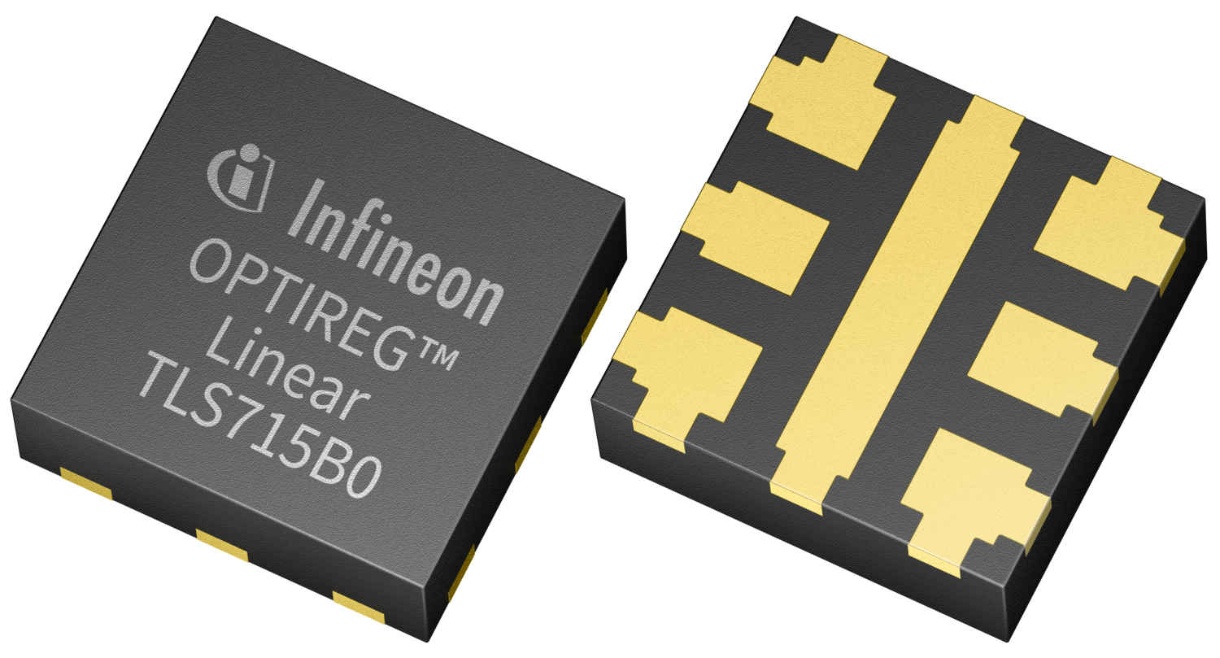
TLS715B0NA V50 – OPTIREG™ Linear Voltage Regulator is a low dropout linear voltage regulator for load current up to 150 mA. An input voltage of up to 40 V is regulated to VQ,nom = 5 V with ±2 % precision. The TLS715B0, with a typical quiescent current of 36 μA, is the ideal solution for systems requiring very low operating current, such as those permanently connected to the battery.
Summary of Features
Wide Input Voltage Range from 4.0 V to 40 V
Output Voltage 5 V
Output Voltage Precision ±2%
Output Current up to 150 mA
Low Current Consumption of 36 μA
Very Low Dropout Voltage of typically 180 mV at 100 mA Output Current
Stable with Small Output Capacitor of 1 μF
Enable
Overtemperature Shutdown
Output Current Limitation
Wide Temperature Range from -40°C up to 150°C
Green Product (RoHS compliant)
AEC Qualified
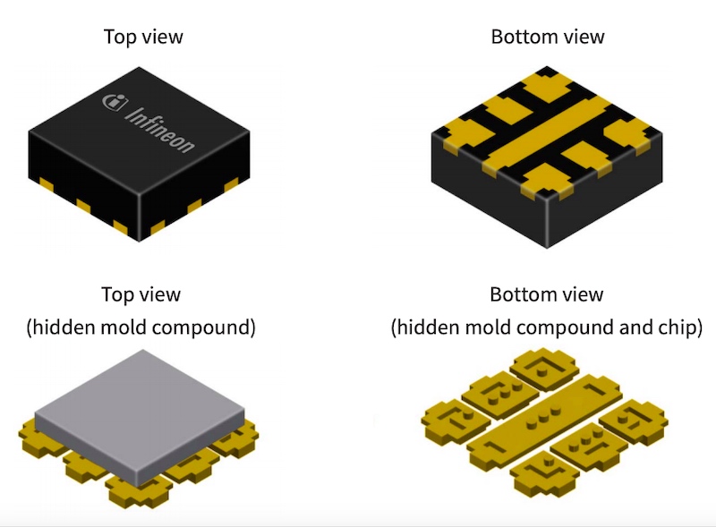
What are Flip-Chips?
With flip-chip technology, the ICs are installed upside down in the package. With the heated part of the IC facing the bottom of the package and being closer to the PCB, thermal inductance can be improved by a factor between 2 and 3. The higher power density enables a significantly smaller footprint than conventional package technologies.
The footprint of Infineon’s new linear voltage regulator (TSNP-7-8 package, 2.0 mm x 2.0 mm) is more than 60 percent smaller than that of an established reference product (TSON-10 package, 3.3 mm x 3.3 mm) while the thermal resistance stays the same. This makes the new device particularly suitable for applications with very limited board space, such as radar and cameras. The OPTIREG TLS715B0NAV50 provides 5 V with a maximum output current capability of 150 mA.
Flip-chip technology has been used in consumer and industrial markets for several years. Due to increasingly strict space requirements, particularly in the growing number of radar and camera systems, also automotive electronics require smaller power supply solutions – albeit with much higher quality requirements. In order to offer best-in-class flip-chip quality Infineon does not rely on a subsequent qualification of existing consumer and industrial products but rather on a dedicated production process for automotive devices.
Low Dropout Voltage
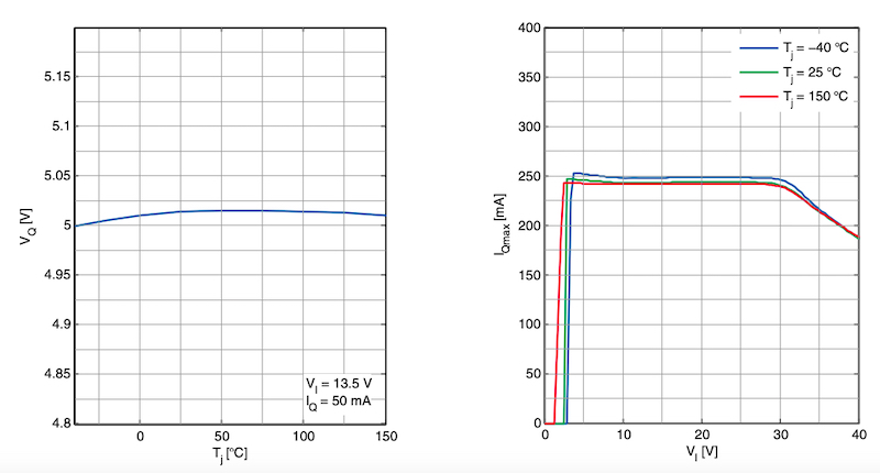
The TLS715BONAV50 features a dropout voltage of 180 mV at output currents below 100 mA. Importantly, the device’s dropout region only begins at an input voltage of 4.0 V.
(Left) Output voltage VQ versus junction temperature Tj. (Right) Output current IQ versus input voltage VI. Image used courtesy of Infineon
This makes the TLS715B0NAV50 an appropriate choice to supply automotive systems with their unavoidable bus voltage fluctuations due to start-stop conditions.
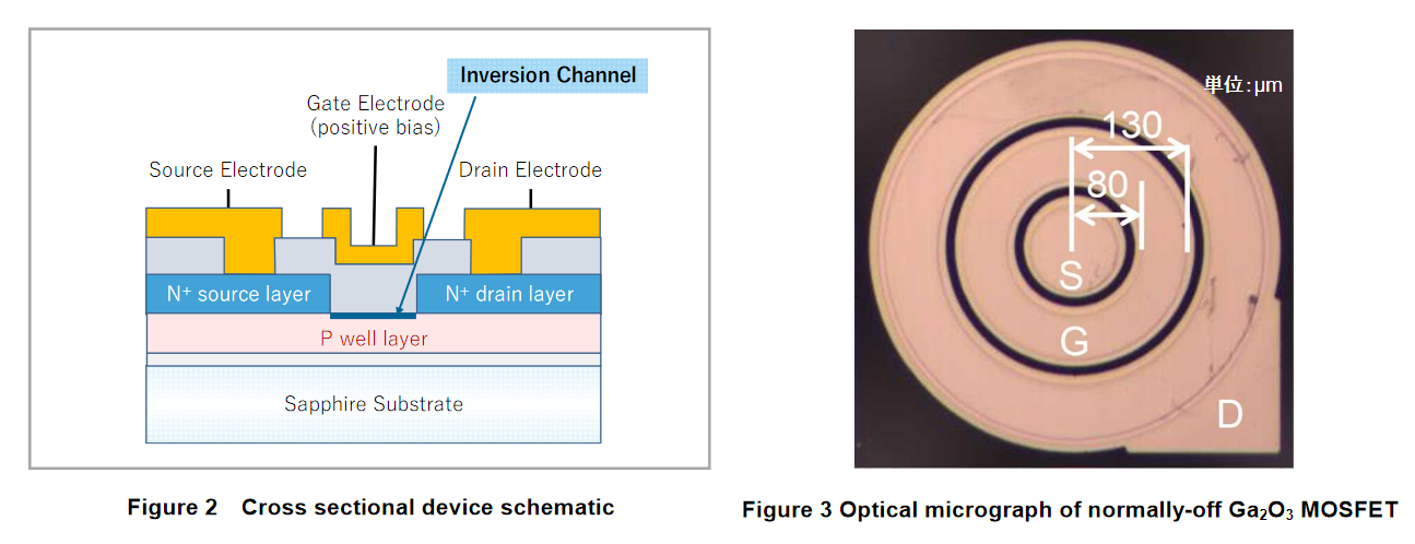
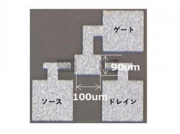
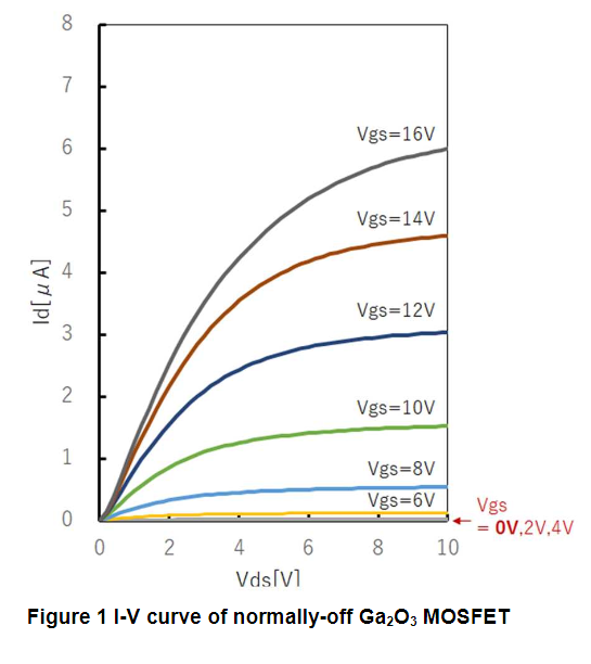
Startup company Flosfia has reported that its gallium-oxide power semiconductor can outperform the characteristics of silicon-carbide, but in a normally-off configuration.
Flosfia Ltd. (Tokyo, Japan), founded in 2011, is a pioneer of the use of corundum-structured gallium oxide (α-Ga2O3) as a power semiconductor. The company said it has achieved a channel mobility of 72cm2/Vs in normal-off operation which it compares to 30cm2/Vs for silicon-carbide.
Whereas other power semiconductors may need the power to be applied to turn-off the transistor having a technology that turns off when no voltage is applied to the gate is an important characteristic of power transistors for safe and secure electrical systems.
Flosfia calculated the characteristic on-resistance of GaO MOSFETs with a withstand voltage of 600V to 1200V by device simulation and found that the on-resistance was approximately 50 percent or less that of commercially available SiC.
Flosfia has signed an agreement with Hakuto and Kyoei Sangyo for these two companies to handle corundum-type gallium oxide power devices as domestic distributors.
A number of smartphone manufacturers have, for a while, been experimenting with E-paper displays with phones like the Hisense A2 and Yota’s Yotaphone 1 and 2 implementing an e-paper based display as a secondary screen. While the use of e-paper displays brought advantages like extended battery life, and reduced pressure on the eyes in bright lights, for phones like the Hisense A2, the addition of a second screen leads to an unavoidable increase in the price of the phones, which made them a bit not attractive to a certain category of the market. To mitigate this and go as bold as guys like Onyx (with the InkPhone), Hisense, announced the launch of a single E-ink Display based smartphone called; Hisense A5.
Hisense A5
The A5 is a relatively affordable Smartphone with a single e-paper that allows the phone to attain a really long battery life. The A5 which runs the Android 9 Pie OS comes with a single black and white 5.84-inch E-Ink Carta display with a resolution of 1440 x 720 and adjustable screen brightness via the built-in front-lit system.
Under the hood, the A5 runs a Qualcomm 660 Octa-core processor, with 4GB RAM and 64GB of internal storage, rounded up with a 13MP rear-facing camera, and a 5MP front-facing camera. All of this is packed into a Black or White colored case (option) and weighs about 158g, majorly due to the non-removable 4000mAh battery, which Hisense says could last up to 10 days on a single charge.
Some of the highlight features of the phone include:
Adjustable front light and a 5.84” multi-touch e-Paper display with 1440 x 720 resolution display
5.0MP front-facing camera and 13.0MP rear camera with flash
3.5mm audio jack, built – in speaker and microphone
802.11a/b/g/n WiFi 4, GPS and Bluetooth 4.2
1 x micro USB OTG port
Non-removable 4000 mAh battery which lasts up to 10days on a single charge
built-in Gravity, Ambient light, and Proximity sensors
Dimensions: 15.41 x 7.46 x 0.80 cm
Like every other smartphone, the A5 also has its plus and minuses. “Liliputing” reports that Hisense A5 has relatively limited support for the US wireless network; the phone only supports some of AT & T, Sprint, T-Mobile and Verizon’s 4G LTE network bands, so depending on where you live, the Hisense A5 may actually serve better as an eReader or small tablet than as a phone. Also due to the slow refresh-rate nature of E-paper displays, the A5 also performs poorly for activities like gaming, video calls, and the likes, as such, it may really be an option for those who are only interested in activities like checking emails, reading e-books, browsing the web and accessing social media platforms.
Lastly, while the device runs on Android, it is important to note that it does not come with Google Play, which means you will have to find a way of getting Google Play on it, or side installs desired apps somehow.
The smartphone is available for sale on Aliexpress for $234 but currently sells for $220 at GearBest, with a pack that includes a manual written in Chinese, a charger, a SIM needle, one USB cable, and one screen protector.
ON Semiconductor’s NCxx333 Zero Drift Operational Amplifiers deliver premium analog performances for front end amplifier circuits and power management designs. A comprehensive choice of packages matching industry-standard pinouts, addressing the various form factor requirements for automotive, industrial, telecom, wearable, Internet-of-Things, test equipment, and instrumentation.
The high analog performance offered by the zero-drift architecture enhances motor control feedback-loop accuracy and power supply control loop contributing to higher system efficiency. The high DC precision parameters of input offset voltage and offset temperature drift makes these amplifiers the ideal choice for low side current sensing and voltage differential measurement on front end sensor functions. The very small voltage variation across temperature coupled with the close to zero offsets ensures the stability of the system operation facing wide temperature exposure without using complex and expensive software calibration algorithms resulting in a more manageable design and product maintenance.
Block Diagram
Features
Gain-Bandwidth Product:
270kHz (NCx2333)
350kHz (NCx333, NCx333A, NCx4333)
Low Supply Current: 17uA (typ at 3.3V)
Low Offset Voltage:
10uV max for NCS333, NCS333A
30uV max for NCV333A, NCx2333 and NCx4333
Low Offset Drift: 0.07uV/°C max for NCS333/A
Wide Supply Range: 1.8V to 5.5V
Wide Temperature Range: -40°C to +125°C
Rail-to-Rail Input and Output
Available in Single, Dual and Quad Packages
NCV Prefix for Automotive and Other Applications Requiring
Unique Site and Control Change Requirements; AEC-Q100 Qualified and PPAP Capable
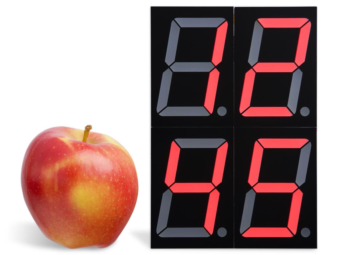
This is a giant digital clock, featuring four large LED displays that provide the time in a format you can read from the other side of the room. by David Johnson-Davies:
This clock was inspired by some 2.3″ one-digit 7-segment displays I saw on AliExpress [1]. I decided it would be fun to have a clock that you can see clearly from a distance. The displays come in a variety of colours and voltages; I chose the red 4V versions so I could drive them directly from the microcontroller’s I/O lines without needing driver transistors. My displays are common-cathode, but a minor change to the program would make it work with common-anode displays.
Big digit 7-segment Clock using ATtiny3216 – [Link]
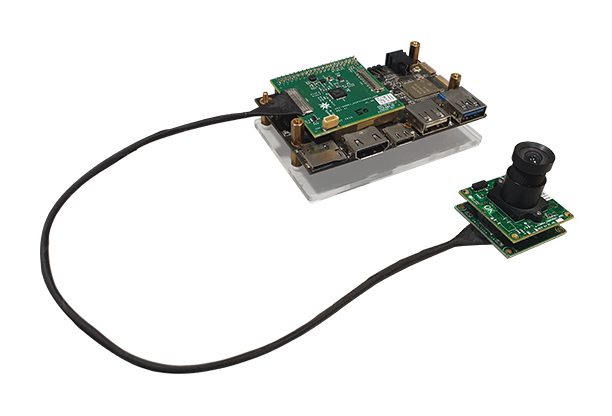
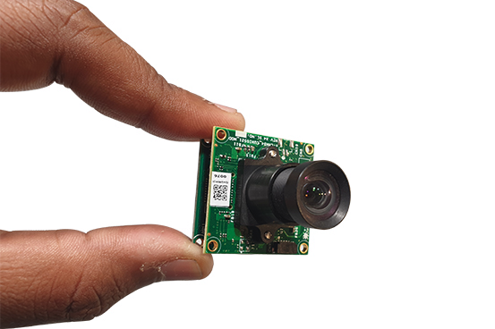
e-con Systems Inc., a leading embedded camera solution company, today announced the launch of e-CAM50_CU96, A lowlight 5MP camera board for 96Boards compliant Rock960 developer kit featuring Rockchip RK3399 processor. e-CAM50_CU96 is based on OnSemi’s 1/2.5″ AR0521, a 2.2 µm pixel CMOS image sensor with integrated Image Signal Processor (ISP).
e-CAM50_CU96 is capable of streaming HD (1280 x 720) at 70 fps, FHD (1920 x 1080) at 60 fps and 5 MP (2592 x 1944) at 25 fps in uncompressed (UYVY). The higher Signal to Noise Ratio (SNR) supported by this camera helps to produce clear images without noise and a better dynamic range helps in retaining more details in shadows and highlights. Along with these features, the powerful in-built ISP helps to bring out the best-in-class video in uncompressed UYVY format. The camera is also provided with the S-mount (M12) lens holder that enables customers to choose the lens from a wide range of options as per their requirements.
e-CAM50_CU96 Camera
The Rock960 platform kit is based on the RK3399 SoC which is a Dual Cortex-A72 + Quad Cortex-A53 CPU, with up to 2 GHZ frequency. This board comes with 4GB RAM, 32GB eMMC, USB3.1 type C, HDMI 2.0, 4 lane CSI-MIPI, etc on the 96Boards Consumer Edition Standard form factor.
With Capability to stream 5MP at 25 fps, Rockchip based Rock960 is a perfect partner for e-CAM50_CU96 to run applications requiring high-resolution images. High-quality video from e-CAM50_CU96 integrated with Rockchip’s powerful multi-core processor enables running of robust vision and image processing applications (Realtime camera vision application eg: Face detection, object identification).
e-CAM50_CU96 Video
Availability
e-CAM50_CU96 is currently available as Engineering samples for evaluation. Customers interested in evaluating e-CAM50_CU96 can request samples from e-con Systems’ online store.
When we are listening to a song, we perceive the sinusoidal sound waveforms as music. Their amplitude gives us how loud the signal is and the frequency tells us if the sound is low or high pitched. However, the third important parameter, which is the phase, is harder to experience by ears.
This tutorial will clarify and give more details about the phase parameter that we already explored in one of our previous tutorials about Phase Splitters. The first section will, therefore, give a presentation of the concepts of phase and phase difference as a reminder.
In the second section, we detail more aspects of the concept of phase shift and we focus on a particular case when the signals are not synchronized.
The third and last section will finally present the important role of the phase difference in the interference phenomenon.
Presentation
The phase of a sine signal is often noted with Φ and measured in radians (rad) or degrees (°) and can vary between -π and +π rad or -180° and +180°.
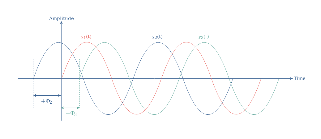
On a graph, the phase of an AC signal represents the initial state of its related sine function at the origin of time :
fig 1: Illustration of three sine waveforms with different phases
The phase Φ of a signal can be of three different nature and dictates the position of the waveform around the vertical axis :
Equal to 0 (° or rad) such as for the signal y1(t) which act as a reference signal
Be positive such as for the signal y2(t)
Be negative such as for the signal y3(t)
The phase of a single signal is not very relevant because whether the AC waveform is of electrical or mechanical nature, the perception will remain unchanged if the signal has a phase or not. What is more important and can clearly be perceived is a phase difference, also called a phase shift between two signals of the same frequency.
Phase difference
Between signals of the same frequency
What is important to keep in mind during this section is that we only talk about a phase shift between two signals with identical frequency. Consider therefore two signals of the same frequency with different phases and possibly different amplitudes: y1(t)=Asin(ωt+Φ1) and y2(t)=Bsin(ωt+Φ2). We define the phase difference as the quantity ΔΦ21=Φ2-Φ1.
In Figure 1, we have ΔΦ21=+Φ2, ΔΦ31=-Φ3, and ΔΦ32=-Φ3-Φ2. A positive phase difference, such as ΔΦ21, indicates that the signal y2(t) temporarily precedes the reference signal y1(t), we also say that y2(t) leads y1(t). A negative phase difference, such as ΔΦ31 and ΔΦ32, indicates that the signal y3(t) follows the signals y1(t) and y2(t), we also say that y3(t) lags y1(t) and y2(t).
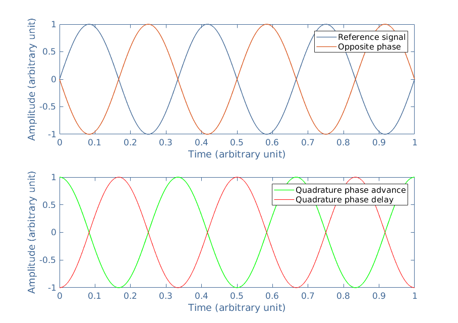
Among all of the values between -180° and +180° or -π and +π rad that a phase difference can take, a few ones can be highlighted and illustrated in the following Figure 2 :
fig 2: Illustration of some relevant phase shifts
An opposite phase is characterized by a phase shift of +180° or +π rad, which is strictly identical to -180° or -π rad. If the reference signal is Vref=vrefsin(ωt), then the opposite signal is Vopp=vrefsin(ωt+π)=-vrefsin(ωt), therefore, Vref+Vopp=0.
Quadrature signals are characterized by a phase shift of +90° or +π /2 rad for the “advance” and -90° or -π /2 rad for the “delay”.
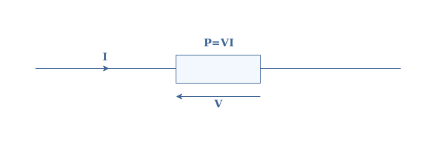
Between the current and voltage signals
In this subsection, we focus specifically on the phase shift of the current (I) and voltage (V) signals across an electrical dipole and investigate its consequences regarding power.
In the DC regime, the dissipated power (P) across a dipole is given by the product of the voltage and current :
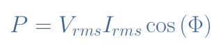
In the AC regime, this representation is no longer true since both the voltage and current are alternating. Consider the voltage across the dipole to be V=Vrms√2.sin(ωt) and the current of the same frequency presenting a phase difference of +ΔΦ: I=Irms√2.sin(ωt+Φ). With Vrms and Irms being the root mean square values.
It can be shown that the active power dissipated in the dipole in AC regime is given by Equation 1:
eq 1: Dissipated power in AC regime
The term cos(Φ) is known as the power factor and gives the efficiency of a receptor to absorb the power of a source. This factor is a real number between 0 and 1 and these two extrema reflect very different behavior :
If cos(Φ)=1 the dipole is considered purely resistive, the phase shift between the voltage and current is zero. The dipole does not present any inductive or capacitive behavior.
If cos(Φ)=0 the dipole is purely reactive, the phase shift between the voltage and current is maximum, equal to ±90° or ±π/2 rad. In this case, the dipole does not consume any power but instead returns it to the circuit.
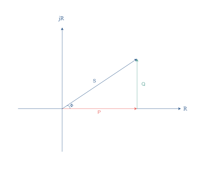
The power given in Equation 1 is called the active power (P), the product Vrms×Irms is known as the apparent power and noted S. It is the power that would be dissipated if the component was purely resistive. The quantity Vrms×Irms×sin(Φ) is the reactive power and noted Q. These quantities can be linked thanks to the phase shift ΔΦ in the same complex power diagram :
fig 3: Definition of the active, apparent and reactive power
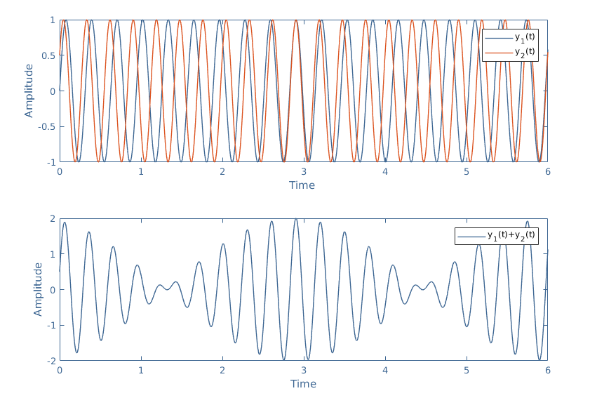
Between signals of similar frequency
In this section, we consider two signals y1(t) which is the reference and y2(t) phase-shifted of Φ of similar frequencies but not strictly identical: ω1≠ω2. Usually, a phase-shift can only be defined for two signals of the same frequency, but in this particular case, it still makes sense to define a phase-difference as the frequencies are similar. If the frequencies are too different, usually when ω1>2ω2 for example, it does not make sense to define it since the phase difference varies as much as the signal itself.
In the case where the signals are of similar frequency, the phase difference is not constant anymore but slowly varies with time: ΔΦ(t)=(ω2-ω1)t+Φ.
The superposition of these two signals is interesting because of the creation of a beating phenomenon such as illustrated in Figure 4:
fig 4: Illustration of the beating phenomenon between two signals of similar frequency
The beating takes his name from the acoustic domain where this phenomenon is particularly audible and easy to experience, however, it also appears in optics, electronics, mechanics etc… The beating is actually a particular case of interference, which we focus on in the next section.
Interference
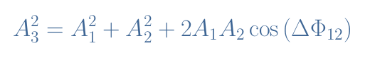
We can see in Figure 4 that a superposition of sine waveforms results sometimes in addition to the amplitudes when the signals are in phase or in a subtraction when the signals are in opposition of phase. This phenomenon is known as interference and takes place when the signals are of the same frequency.
Consider again two sinusoidal waveforms of identical frequency : y1(t)=A1sin(ωt+Φ1) and y2(t)=A2sin(ωt+Φ2). Let’s call y3(t) the superposition y1(t)+y2(t) and A3 its amplitude. It can be shown that the amplitude of y3(t) satisfies the following equation :
eq 2: Amplitude of the superimposed signal
We can notice that the phase difference between y1(t) and y2(t) plays an important role in the final amplitude of the resulting signal. Two cases are interesting to highlight :
ΔΦ12=0, the signals are in phase and the amplitude A3 is maximal as satisfies A32=(A1+A2)2. In this case, we say that the interference between y1 and y2 is constructive.
ΔΦ12=±π rad, the signals are in opposition of phase and the amplitude A3 is minimal and satisfies A32=(A1-A2)2. In this case, the interference between y1 and y2 is destructive.
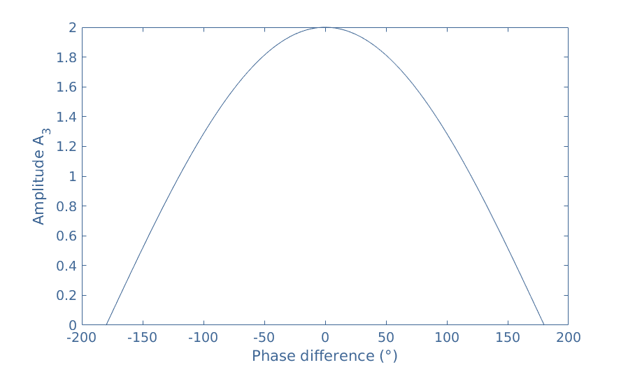
When the phase difference is between these two extrema, we can plot a graph showing the evolution of A3 as a function of ΔΦ12 :
fig 5: Amplitude of the resulting signal as a function of the phase difference
In this figure, we choose for the sake of simplicity A1=A2. We can see again that when ΔΦ12=0, A3=A1+A2=2 and when ΔΦ12=±180°, A3=A1-A2=0.
Conclusion
This tutorial has given a detailed presentation about the concept of phase and phase difference, moreover, it has pinpointed its importance through some examples.
First of all, we present what is the phase of a signal and in which unit it is measured. The concept of phase alone, however, is not very relevant and this is why we focus on the following sections about the phase difference or phase shift.
In the first paragraph of the second section, we define the phase shift ΔΦ and give some vocabulary related to particular cases of phase difference: in-phase (ΔΦ=0°), the opposition of phase (ΔΦ=±180°) and the quadratures (ΔΦ=±90°).
In a second subsection, we highlight the importance of the phase-shift between the current and voltage in a circuit. The power dissipated in any electronic component is directly proportional to the cosine of the phase shift, which is called the power factor.
In the last section, we link and explain the interference phenomenon to the phase shift parameter. The beating phenomenon which is explained previously in the article is a particular case of interference.