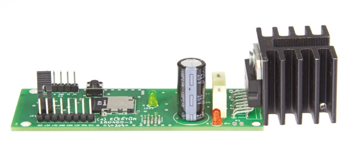
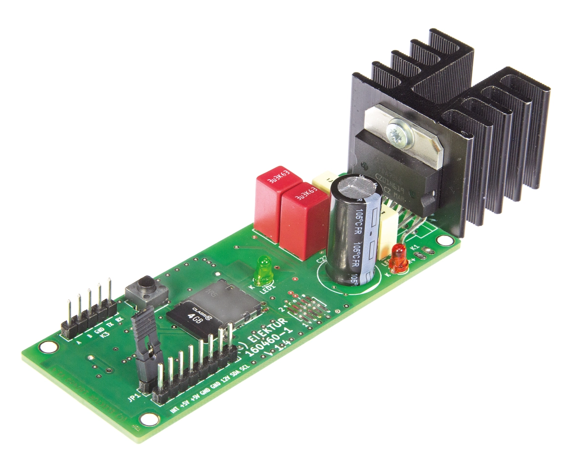
With a smartphone or an MP3 player it’s easy to play audio files, but generally not at room strength or if you can, only in wretched quality. The Card Sound project makes it possible to fill the room with music and have excellent sound reproduction! This lightweight and compact player also stands out for its modest quiescent current consumption and desirable extra features such as I²C and RS-485 control.
Quick Features:
Analogue/digital supply voltages: 3 to 18 VDC / 4.5 to 12 VDC
Analogue/digital current requirements: see Measurements panel
Sinewave output power Pout into 4 or 8 Ohm: 12.5 W or 6.25 W (measured at 10.0 V peak-to-peak)
Output: short-circuit protected max. 2 A
Harmonic distortion: see Measurements panel
Zero-value noise: around 1.4 mW
Data formats: PCM 16, 24, 32-bit for each of 32, 44.1, 48, 96, 128 kHz Stereo
Dimensions (L x W x H): 89 x 33 x 30 mm
Weight without SD card: 26 g
Figures valid with a supply voltage of 5 VDC (digital) and 12 VDC (analogue) for a 1 kHz sinewave signal with 16 bits and 44.1 kHz sampling rate
Article Details:
Original publication: Elektor magazine issue 1/2018 on page 44.
Author: Falko Bilz
Free download expires: Friday 31 January, 2019.
Original article production number: 160460
PCB available: yes, see Products below
Like what you’re seeing? Then go to the article page and download a pdf copy of the full, original article. Downloading is free from Friday 24 January to Friday 31 January 2020.
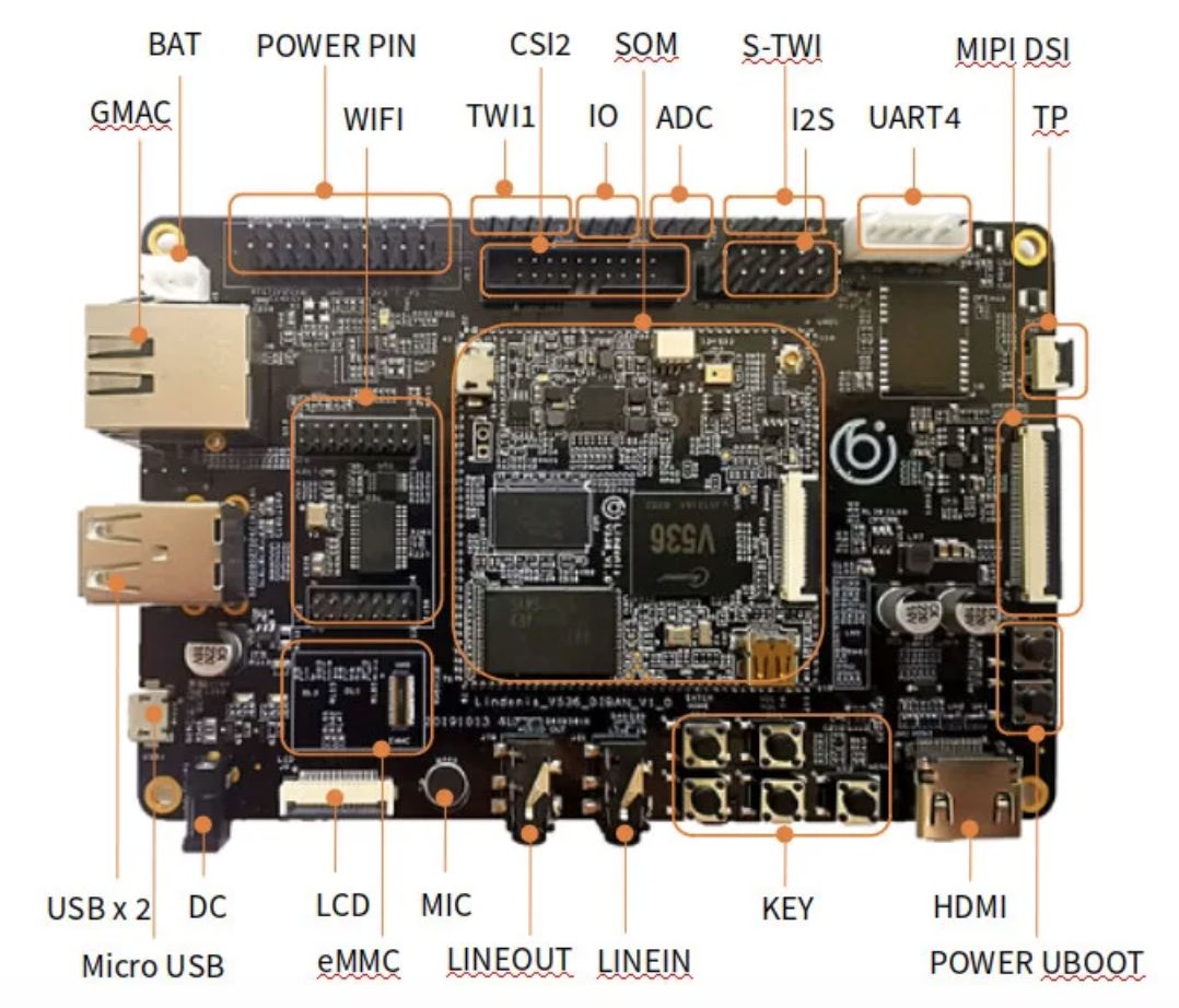
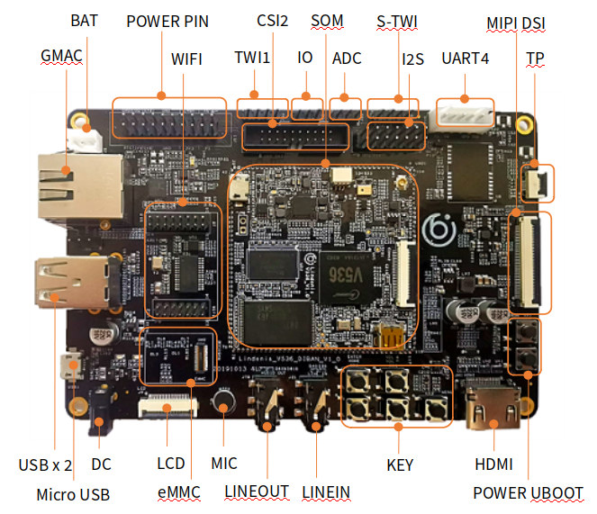
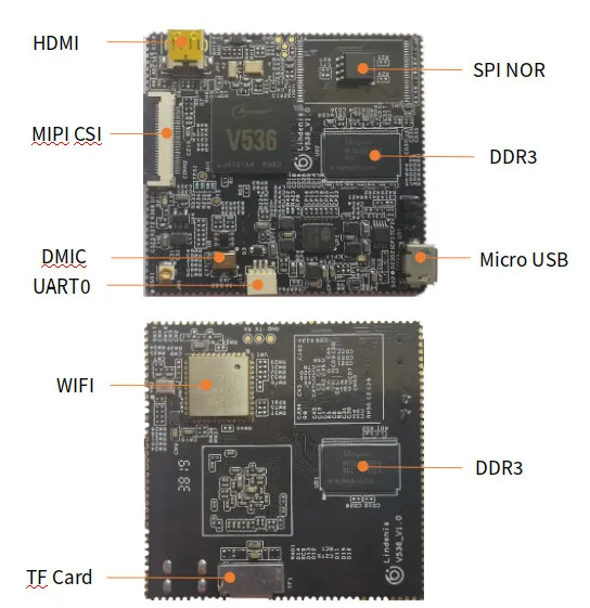
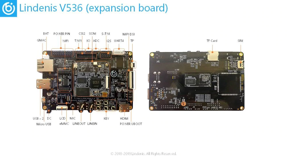
Similar to the earlier Lindenis V5 designed for AI video processing and 4K encoding, Lindenis has released another single-board computer that uses SoM and baseboard design for 4K camera applications called the Lindenis V536.
The Lindenis V536 which runs on a new Allwinner dual Cortex-A7 processor and a single MIPI SCI interface was designed for applications that rely heavily on popular open-source packages such as Live555, V4L2, FFmpeg and custom framework, and libraries. Capable of doing a lot on image signal processing and video encoding/decoding functions, the Lindenis V536 is suitable for sample applications like 4K camera applications, media player applications, and low-latency A/V streaming applications. It supports functions like image mirroring and flipping, color enhancement and adjustment, bad pixel, and lens shading correction, providing ISP tools for the PC, contrast and sharpness enhancement, motion smear and color noise removal, real-time multi-stream encoding capability, eight ROI encoding as well as MJPEG / JPEG baseline encoding.
Hardware features and specifications include:
Expansion board
Dimension: 130 x 85mm
1 DVP connector for camera input
eMMC flash module connector and MicroSD card slot for storage
Analog microphone and 3.5mm line in and out jacks for audio
14-pin I2S header, 3-pin ADC header, 3-pin EINT – GPIO header and 4 –pin TWI header with 1 TWI and S-TWI each
Power supply – 5V/2A micro USB connector, 5V/2A via DC jack, 3.7V battery connector, and 20-pin power supply header
Core Board
50 x 50mm in size
1GB DDR3 for system memory
Allwinner V536 dual-core Cortex –A7 processor @ 1.2 GHz and 4K H.265/H.264 video decoding and encoding @30 fps, 28nm process
SPI NOR flash or SPI NAND flash, bootable MicroSD card for storage
MIPI CSI connector and MIPI HDMI 1.4 port for video input and output
Digital microphone for audio
802.11b/g/n/ac Wi-Fi 5 and Bluetooth 4.2 via AP6255 for connectivity
Baseboard Interface – Castellated holes
Power supply: 5V/2A via micro USB port or castellated holes
The Lindenis V536 also comes with an SDK that includes an OpenWrt with Linux 4.9, Arm GCC based cross-toolchain, U-Boot 2014.07 and an integrated build system. It is sold for a regular price of $52 while the SBC is sold for $94 together with other accessories like the HDMI cable, flash module, camera module, and Bluetooth/Wifi module.
More about the board and the SDK can be found on its wiki page.
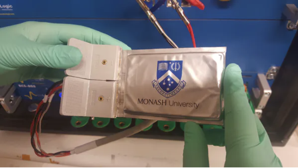
What would you give for a battery, 5x the storage capacity of whatever you’re reading from? Well, the countdown to commercial availability for batteries of this type of capacity has already begun and it would be considerably cheaper than then currently available batteries.
This radical improvement comes from using sulfur cathodes rather than graphite in lithium-ion batteries. Sulfur ranks high on the list of very abundant materials and is relatively cheap to produce unlike rare minerals like cobalt used to produce regular lithium-ion batteries. So why didn’t anyone think of this until now?
Actually, it’s pretty well known that lithium-sulfur batteries can store far more energy than their lithium-ion counterparts, six-times in theory. However, the battery’s performance degrades quite rapidly due to its high storage capacity (That’s six times the stress—pretty understandable), as the sulfur cathode is nearly double its usual size when the battery is fully charged which destroys electron paths in the binder across the electrodes. As a result of this, repeated charging and discharging lead to rapid deterioration of the batteries’ performance.
Solving this problem was the goal of a research team at Monash University led by Mahdokt Shaibani, and their efforts have led to the development of a new technique for processing lithium-sulfur batteries that allows them to undergo hundreds of charge-discharge cycles without breaking down. Attaining a level of stability that is already being considered as a huge breakthrough in battery technology.
The team’s technique involved tweaking the process of making lithium-ion batteries just a little differently so that the binder across the electrodes can accommodate the expansion of the sulfur electrodes. In an article published to explain their work, Mahdokt Shaibani said:
“To make sure our batteries would be easy and cheap to manufacture, we used the same material as a binder but processed it a little differently. The result is a web-like network of binder that holds particles together but also leaves plenty of space for the material to expand. These expansion-tolerant electrodes can efficiently accommodate cycling stresses, allowing the sulfur particles to live up to their full energy storage capacity.”
The Research Team (Credit: Monash University)
The approach adopted by the team not only favors high-performance long cycle life but also simplifies manufacturing and reduces associated cost, along with a significant reduction in hazardous waste thanks to the water-based nature of the process.
The research team includes Professor Mainak Majumder (Monash University), and Associate Professor Matthew Hill (CSIRO and Monash University) who is renowned for translating laboratory success to industrial application in record time, which is somewhat our hope for this breakthrough.
The study was published on Science Advances on Saturday, 4 January 2020. More information on the research can be obtained from the publication.
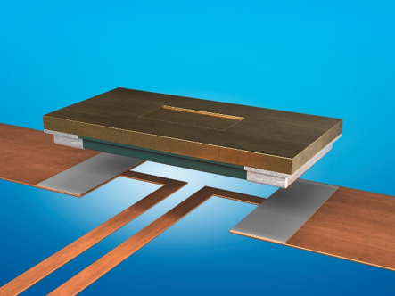
Isabellenhütte has developed a new range of precision resistors in standard sizes with resistances ranging from 1 to 6 mOhm for applications that require small and low-ohmic shunts. In terms of their construction, the components are also less complex than the current ISA-PLAN®resistance families. And yet, they offer the same performance quality: very good long-term stability, a low temperature coefficient, and low thermoelectric voltages.
With the FMx shunt family, Isabellenhütte has now plugged a gap in the standard size range for precision resistances. It has not been possible with the previous product ranges to realize the usual S (2512), P (2010) and K (1206) standard sizes in the resistance range from 5 to 1 mOhm. The impetus for this new development was provided by increasing demand for these resistances as well from a wide range of industries, including the automotive sector (for in-car chargers and assistance systems) and industry (for BLDC drive units), but also from the consumer market (e.g. for white goods).
The development approach
The large cross-sectional areas required for low-ohmic components have been achieved by a change in construction, and the production process has also been significantly simplified. A further milestone for the FMx shunts has been the development of the NOVENTIN® resistance alloy to make it possible to realize these low-ohmic values in defined sizes. Until now, the ISA-PLAN® resistances (SMx, VMx and CMx) have followed a sandwich construction, consisting of a substrate – usually copper – an adhesive and a resistance film made out of the ZERANIN® and MANGANIN® resistance alloys developed in-house by Isabellenhütte. The FM in the title of the new range stands for “Full Metal”, i.e. the components are fashioned in the corresponding thickness out of a full metal plate made of the resistance material in question and directly soldered onto the underside. These variant is very low-ohmic due to the large cross-sectional areas. 1 mOhm is realized with the ZERANIN® alloy, 2 mOhm with MANGANIN®, and, for the first time, NOVENTIN® is being used in ISA-PLAN® products for the resistance range from 3 to 6 mOhm. The new design has given rise to a particularly robust construction which also makes it possible to leave out some work stages and reduce costs. An important point for the automotive industry is this: The components form a soldering point meniscus to guarantee the possibility of automated inspection of the soldering points.
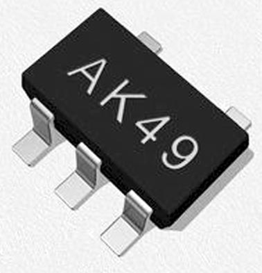
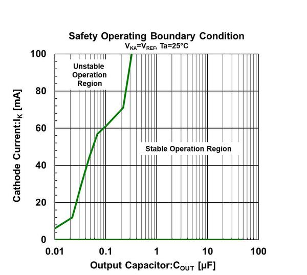
NJR provides samples of a new adjustable shunt regulator NJM17431 with high precision and wide stable operation region that has been designed by latest process and analog circuit technology for many years.
Because the NJM17431 has 0.8% accurate voltage reference and wide stable operation region for large capacitive load, it can be used for a very wide range of applications. And it can replace Zener diode with the NJM17431.
Since the stable operation region is wide, it will help engineers reduce the design man-hours and the burden of replacement evaluation.
The NJM17431 operates stable in the range of 0.01 μF to 100 μF with the actual usage cathode current region.
Characteristics
Reference Voltage Tolerance: 2.5 V±0.8%
Adjustable Output Voltage: VREF to 36 V
Wide Stable Operation Region
Low Temperature Coefficient of Voltage Reference
The output voltage can be set with two external resistors
Bipolar Technology
Package: SOT-23-5
The part will enter mass-production in the second quarter of 2020. More information: www.njr.com
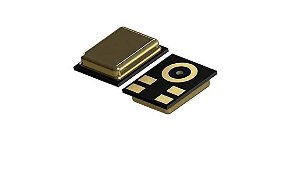
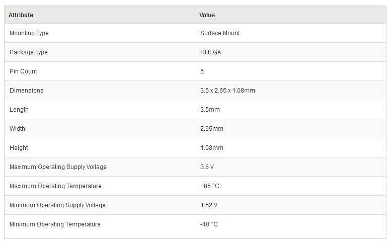
The MP23ABS1 is a compact, low-power microphone built with a capacitive sensing element and an IC interface. The sensing element, capable of detecting acoustic waves, is manufactured using a specialized silicon micromachining process to produce audio sensors. The MP23ABS1 has an acoustic overload point of 130 dBSPL with a typical 64 dB signal-to-noise ratio. The sensitivity of the MP23ABS1 is -38 dBV ±1 dB @ 94 dBSPL, 1 kHz.
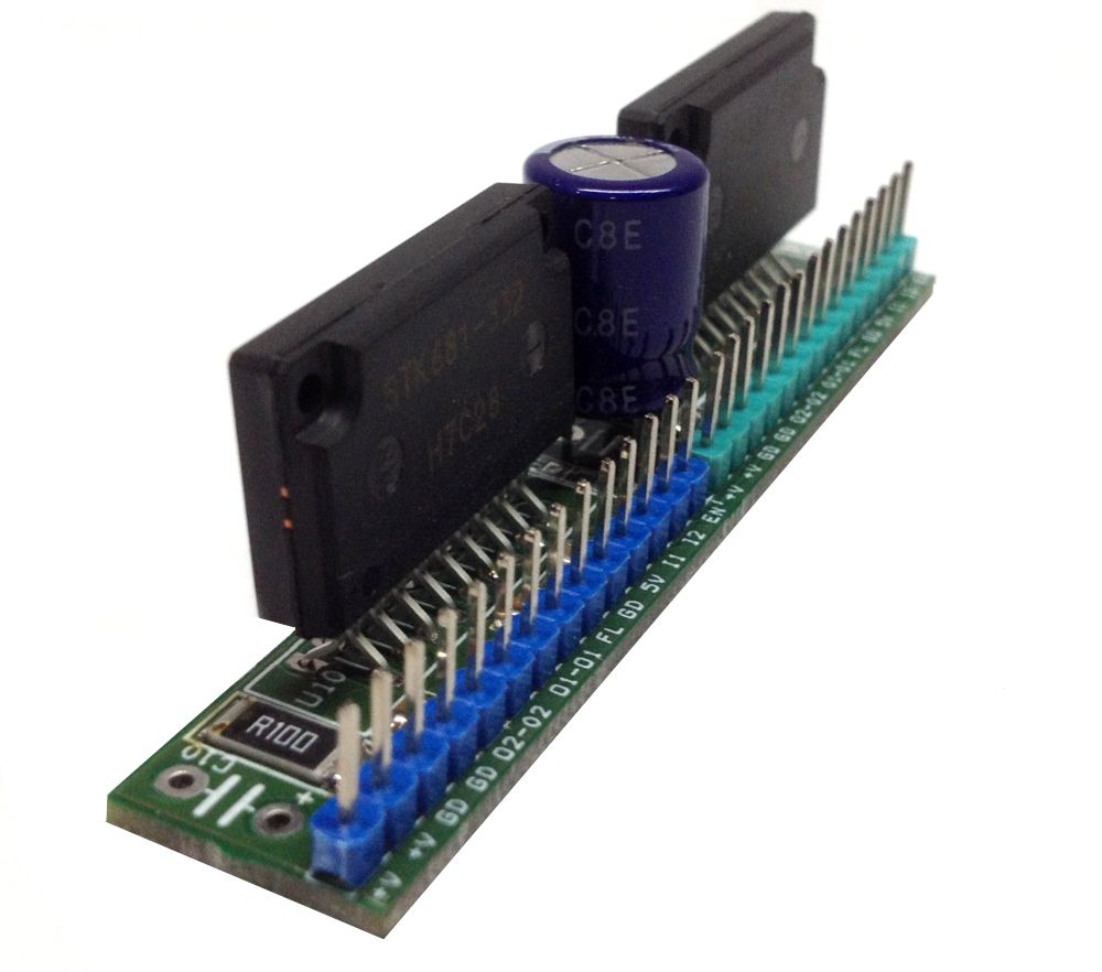
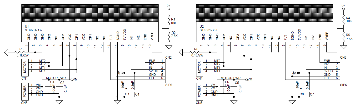
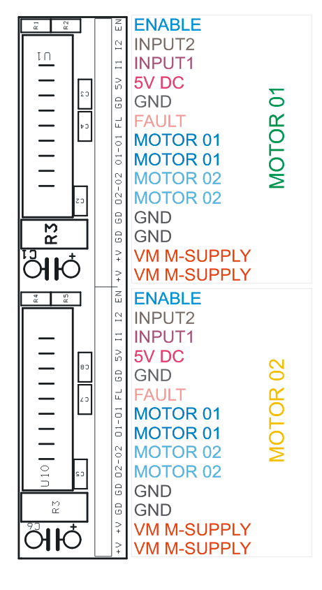
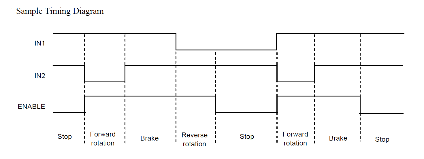
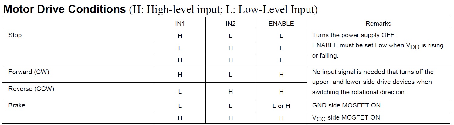
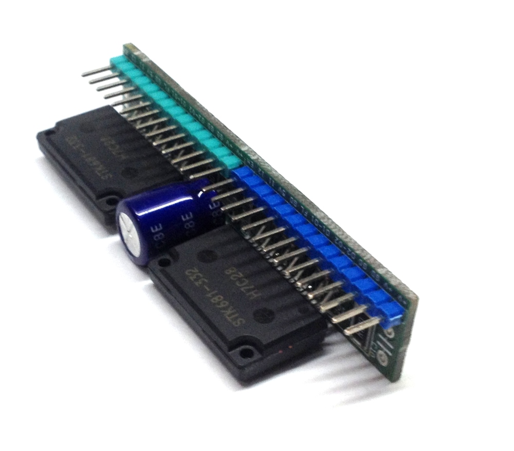
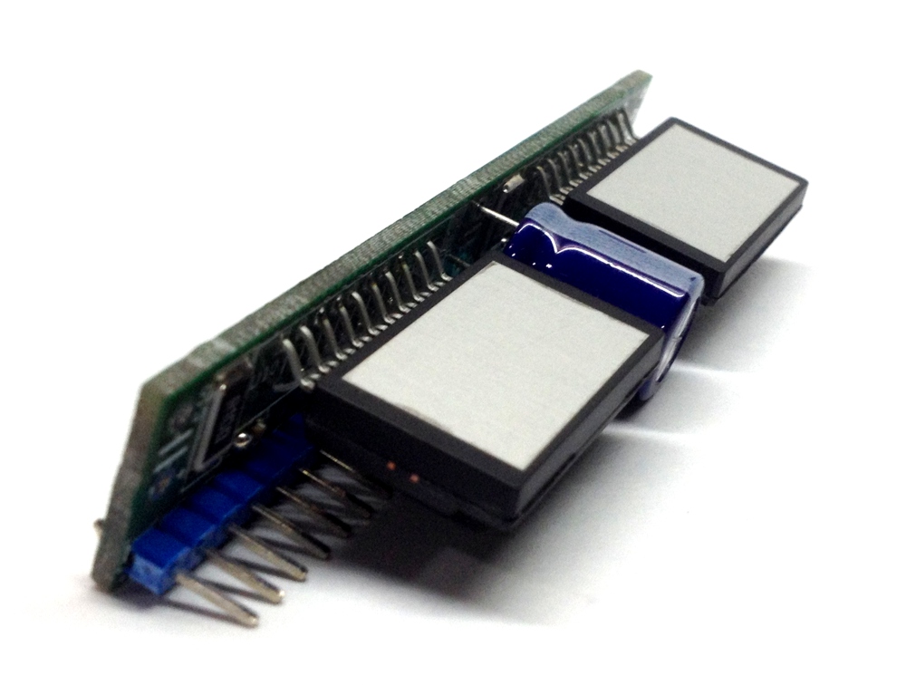
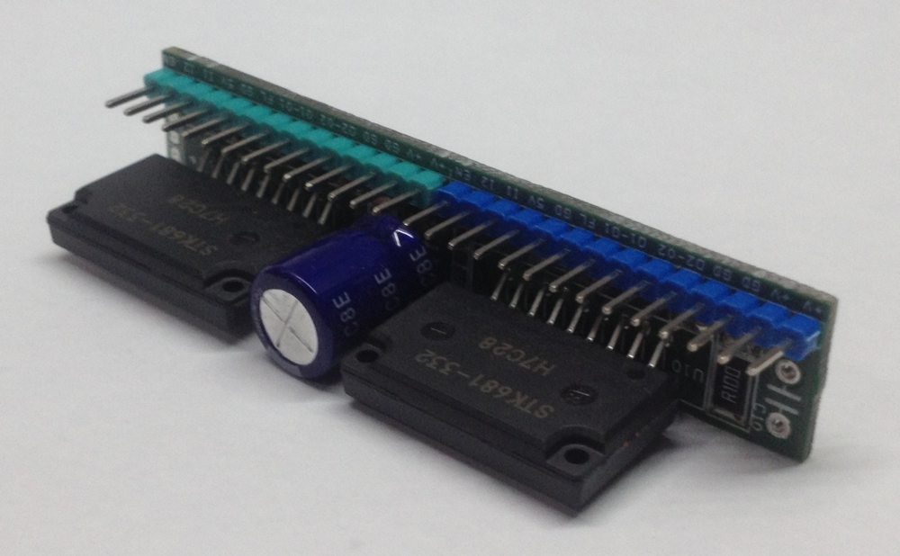
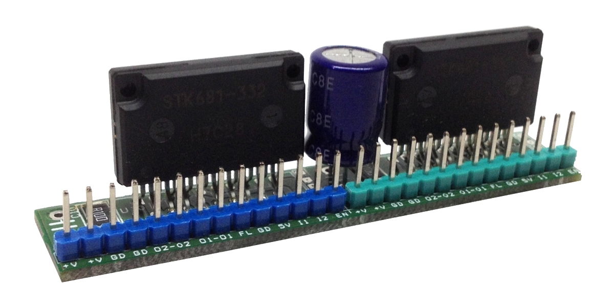
This high current forward-reverse DC motor driver is built using STK681-332 IC from ON Semiconductor. The circuit can drive brushed DC Motor with up to 12 A peak current. The circuit requires 3 input signals: Enable for PWM input for speed control, IN1 and IN2 to change the motor direction and to apply the brake while the motor is in running condition. Monitor (Fault) pin is used when either of the outputs short-circuits detector, overcurrent detector, or overheat detector is activated. When the detector is activated, this pin is set low and all outputs are latched off. If the output pin is short-circuited directly to VCC or connected directly to GND, an output short circuit condition is detected and the output is latched in the off state. To restart the operation, turn on 5V supply again. The maximum input frequency is 50 kHz. Both ICs required a large size heat sink to dissipate heat.
Dual Forward/Reverse DC Motor Driver with Brake for Robots – [Link]
This high current forward-reverse DC motor driver is built using STK681-332 IC from ON Semiconductor. The circuit can drive brushed DC Motor with up to 12 A peak current. The circuit requires 3 input signals: Enable for PWM input for speed control, IN1 and IN2 to change the motor direction and to apply the brake while the motor is in running condition. Monitor (Fault) pin is used when either of the outputs short-circuits detector, overcurrent detector, or overheat detector is activated. When the detector is activated, this pin is set low and all outputs are latched off. If the output pin is short-circuited directly to VCC or connected directly to GND, an output short circuit condition is detected and the output is latched in the off state. To restart the operation, turn on 5V supply again. The maximum input frequency is 50 kHz. Both ICs required a large size heat sink to dissipate heat.
Features:
DC Supply Input Up to 48V DC
Maximum Peak Current 12Amp
External current detection resistor allows overcurrent detection and peak current control in the PWM operation mode.
Maximum Operation Frequency 50Khz
Allows forward, reverse, and brake operations in accordance with the external input signal.
12A peak startup output current and 12A peak brake output current.
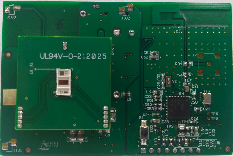
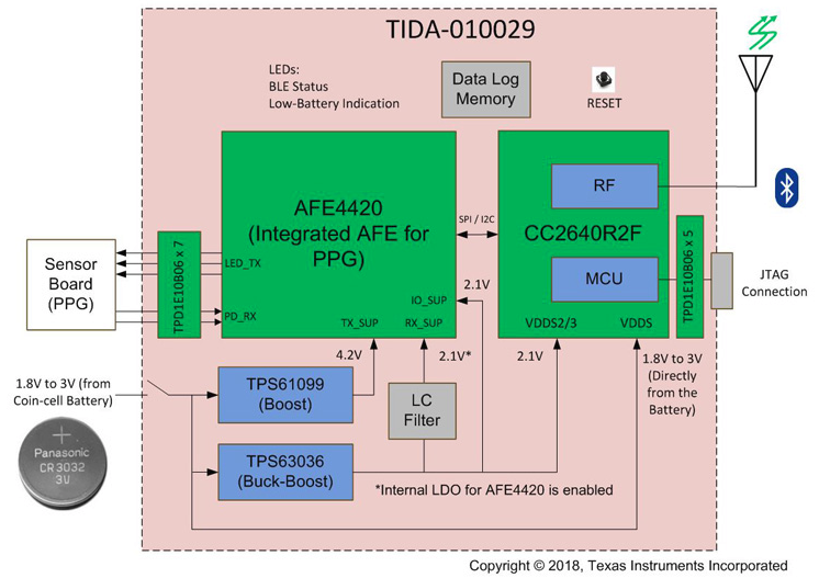
This reference design enables a wearable, optimized saturation of peripheral capillary oxygen (SpO2) and multi-sensor, multi-wavelength optical heart rate monitor (HRM). It uses AFE4420 device, which is a single-chip, bio-sensing front end for photoplethysmography (PPG) measurements. It supports up to four switching light-emitting diodes (LEDs) and up to four photodiodes to enable signal acquisition of up to 16 Phases. The CC2640R2F device (supporting Bluetooth® low energy 4.2 and 5) transfers the measured data to a remote location. This patient-monitoring design uses a single CR3032 battery with a 30-day life cycle. Raw data is available to calculate heart rate, SpO2, and other related parameters. 2 onboard light-emitting diodes (LEDs) identify low-battery detection and a Bluetooth connection.
Features
Provides raw data to calculate heart rate, SpO2, and other related parameters
Uses single-chip, bio-sensing, front-end AFE4420 device for PPG measurement
Supports up to 4 LEDs and 4 photodiodes with ambient subtraction to improve signal-to-noise ratio (SNR)
Enables signal acquisition of up to 16 phases and multi-wavelength measurements with the flexible allocation of LEDs and photodiodes in each phase
Integrated Arm® Cortex®-M3 and 2.4-GHz RF transceiver (CC2640R2F) supports wireless data transfer through Bluetooth® low energy 4.2 and 5.0
Operates from CR3032 (3-V, 500-mA coin cell battery) with a battery life of 30 days using highly efficient DC/DC converters
Small form factor helps in easy adaption to wearable applications
Block Diagram
TIDA-010029 Wearable, 16-phase multi-sensor SpO2 and heart rate monitor (HRM) reference design with Bluetooth® 5 block diagram image
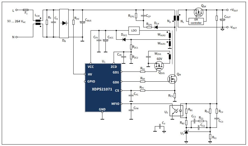
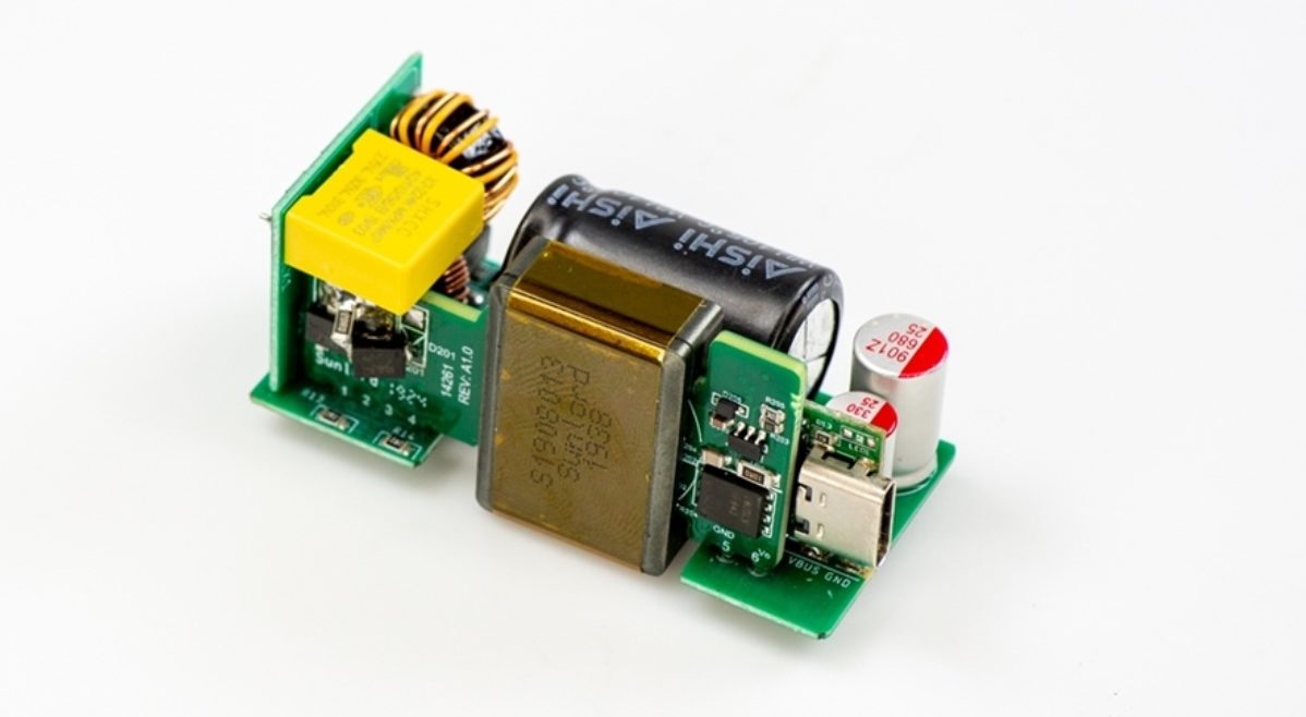
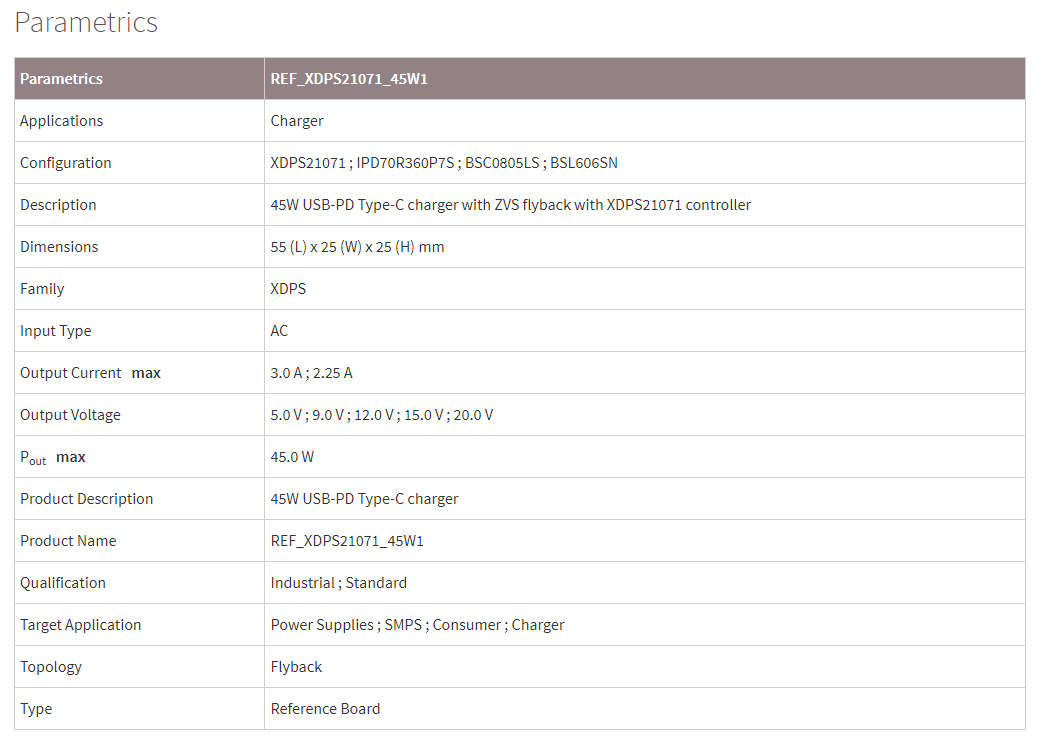
The REF_XDPS21071_45W1 from Infineon is a 45W USB-PD type C charger reference design in a small form factor. The reference design has been developed to demonstrate the performance by meeting various regulatory limits as well as allowing for small form factor designs.
It features Infineon’s digital flyback controller XDPS21071, 700V CoolMOS™ P7 Superjunction MOSFET (IPD70R360P7S), OptiMOS™ PD synchronous-rectification MOSFET (BSC0805LS) and small-signal-MOSFET (BSL606SN).
This 45W USB-PD 3.0 type C charger has a universal input voltage range of 90- to 264-Vac. The supported output is 5V/3A, 9V/3A, 12V/3A, 15V/3A and 20V/2.25A. Its peak efficiency is 90%, with a low standby input power of <30mW.
Circuit Overview
The REF_XDPS21071_45W1 circuit is similar to a typical flyback converter design with SR in the secondary high-side. The XDPS21071 is a cycle-by-cycle peak current flyback controller with secondary-side control by means of a MFIO pin. The particular design can achieve close to ZVS with the help of an additional ZVS winding and ZVS circuit driven by the GD1 pin.
Simplified circuit diagram
With the ZVS feature, the switching loss is reduced significantly at high-line so that the switching frequency can be set at around 140kHz. For low-line, the system would run in DCM operation. Besides having high efficiency at full load, the controller can achieve high efficiency at both medium and light load by implementing FRM and ABM. The controller integrates a HV start-up cell. Connected with a resistor, RHV (102kΩ) from the bulk capacitor, it can achieve VCC start-up charging and also the brown-in and brown-out features.
In addition, it has various protection features to protect the system from hazards, such as OCP, Vout OVP, OLP, OTP, latch enable, CS pin short before power-up, etc.
Summary of Features
High density with 21.5W/in3 PCBA design
High efficiency with adaptive ZVS operation and frequency law for variable output design
DCM operation design
Small form factor with planar transformer design
Brown-out, output short, overload and output overvoltage protection