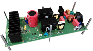
SECO-1KW-MCTRL-GEVB is a Compact Intelligent Power Module (IPM) Motor Drive
The SECO-1KW-MCTRL-GEVB is a complete reference design for three-phase motor drives, featuring the NFAQ1060L36T intelligent power module in a DIP/6 package. Rated for 230 Vac input and delivering up to 850W. All the necessary system blocks for a motor drive are part of the solution: EMC filtering and rectification stage, interleaved two-channel PFC, auxiliary power supplies, three-phase inverter and measurement and protection. The graphical user interface ensures an easy startup for evaluation purposes running voltage/frequency control. Furthermore, the system can accommodate additional control strategies.
Features
850W Intelligent Power Module (IPM) three-phase motor driver
VIN: 230 Vac,rms ± 15% (single-phase)
IOUT: Irms 10 ARMS per phase
Compatible with three-phase motors: PMSM, BLDC or ACIM
DIP/6 IPM NFAQ1060L36T, three-phase/10A with integrated gate drivers
Cross-conduction, overcurrent and thermal protection embedded in DIP/6 module
Plug-in connector interface for MCU cards (Arduino DUE footprint)
Voltage/frequency control strategy implemented
NCS2250SN2T3G: Push Pull Output Comparator implemented in Itrip protection system
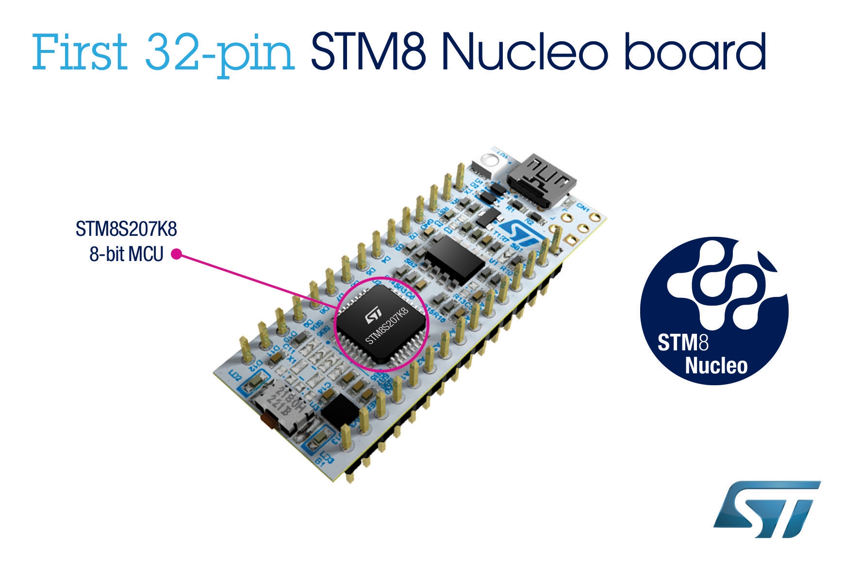
STMicroelectronics is making design starts using 8-bit STM8 microcontrollers (MCUs) faster, more affordable, and more accessible for creative minds of all types by introducing new development boards in the easy-to-use Nucleo-32 form factor.
The compact boards are controlled and powered conveniently through a USB connection. An ST-LINK debugger/programmer is integrated, which saves using an external debug probe and allows simple drag-and-drop Flash programming. Arduino™ Nano pins simplify functional expansion using off-the-shelf shields and let users connect with open-source hardware communities. The boards are supported by major development toolchains including IAR Embedded Workbench for STM8 and Cosmic CXSTM8.
STM8 MCUs feature a high-performing 8-bit core, generous on-chip memory including up to 128Kbyte of Flash, and state-of-the-art peripherals shared with the STM32 MCU family such as timers, analog peripherals, CAN2.0B, and digital interfaces. The STM8 MCUs are a popular choice for creating smart sensors, actuators, and other products within tight power, space, and cost constraints.
The first available STM8 Nucleo-32 board, the NUCLEO-8S207K8, contains a 32-pin STM8S207K8 MCU, which provides features including 12 high-current outputs and multiple capture-compare channels.
Features of the NUCLEO-8S207K8 STM8 Nucleo-32 board include
STM8S207K8T6C microcontroller in LQFP32 32-pin package
4 LEDs:
USB communication
Power
User
Default
1 reset push-button
Board connectors:
ARDUINO® Nano V3 expansion connector
Micro-B USB connector for the ST-LINK
SWIM interface
Flexible power-supply options: ST-LINK USB VBUS or external sources (3.3 V, 5 V, 7 V – 12 V)
On-board ST-LINK/V2-1 debugger/programmer with SWIM connector and USB re-enumeration capability: mass storage, Virtual COM port and debug port
Comprehensive free software STM8 libraries including a variety of software examples
Support of a wide choice of Integrated Development Environments (IDEs) including STMicroelectronics free STVD-STM8 (using Cosmic toolchain), IAR™, Cosmic free IDEA
It’s becoming quite obvious that traditional batteries are limiting the progress of IoT devices. They are expensive, they contain harmful chemicals and most importantly All-Batteries-Will-Die. Vemund Kval Bakken chief technology officer and co-founder at ONiO say the real problem with the battery approach to IoT comes when you actually consider the battery shelf life as well as the environmental aspects. A battery shelf life between 5 to 10 years means that 99% of the batteries’ capacity was depleted during storage. The shelf life degrades significantly to less than 5 years in temperate regions due to much higher leakage. There are obvious solutions to this problem, you could just use a charger, or, you could use very specific battery topology or chemistry. Both make the devices quite expensive and difficult to export. They hinder the Deploy and Forget vision for IoT devices.
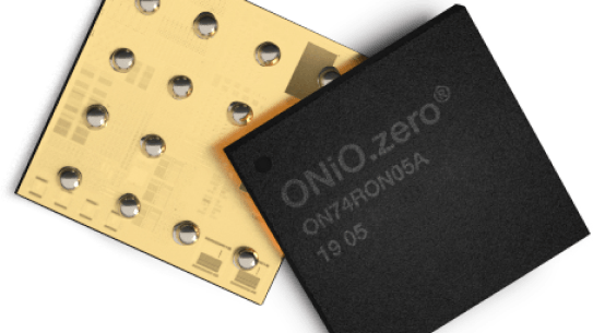
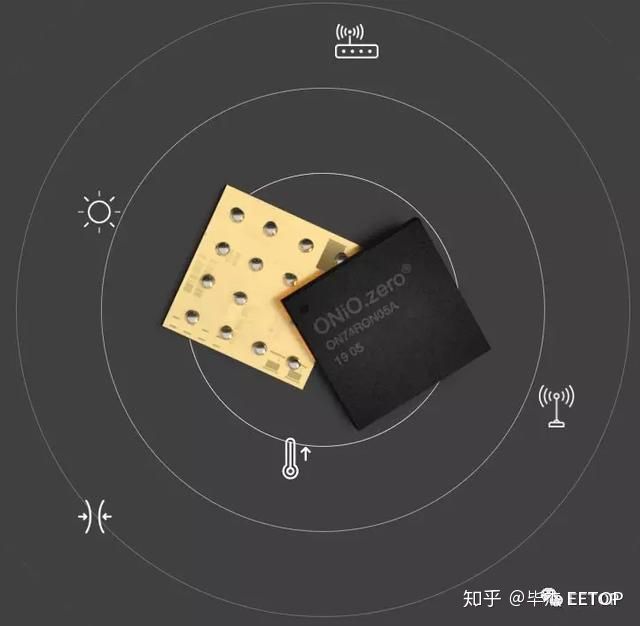
ONiO.zero MCU
His team has created ONiO.zero to address this problem. In their own words,
“ONiO.zero is an ultra-low-power wireless microcontroller that uses energy harvesting technology. It operates solely with energy from its surroundings. No coin-cell, no supercapacitor, no lithium, no battery at all”.
In practice, there are no limitations on the lifetime of the chip. Also, while traditional solutions require about 15 external components and inductors to work. ONiO requires just one. This implies tremendous savings for your Bill of Materials.
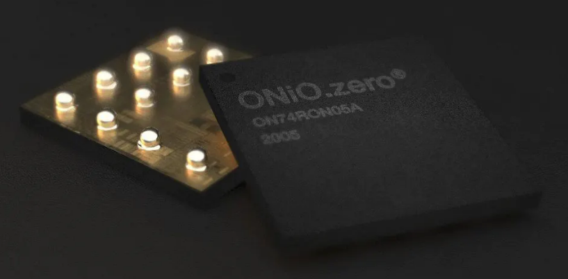
ONiO.zero harvests energy from it’s surrounding
The real promises here are fewer components and smaller designs, which is needed in a wide range of solutions, watches, wearables, machine parts – you name it. But more importantly, it means greener and more climate-friendly devices.
Programmable output power (-40 to 0dBm). PA supports operation down to 850mV – 0dBm. IEEE 802.15.4 UWB transmitter. 3.5 to 10GHz.
Optional 433MHz MICS radio transmitter for medical devices.
Peripherals
Industry Standard I2C, SPI and UART.
Asynchronous AES module for encryption/hash generation.
GPIO with asynchronous interrupt/wake up.
Programmable current source.
Biasing external sensors.
At the time of writing, ONiO.zero is not yet commercially available but you can find more information and monitor its progress via its Official product page.
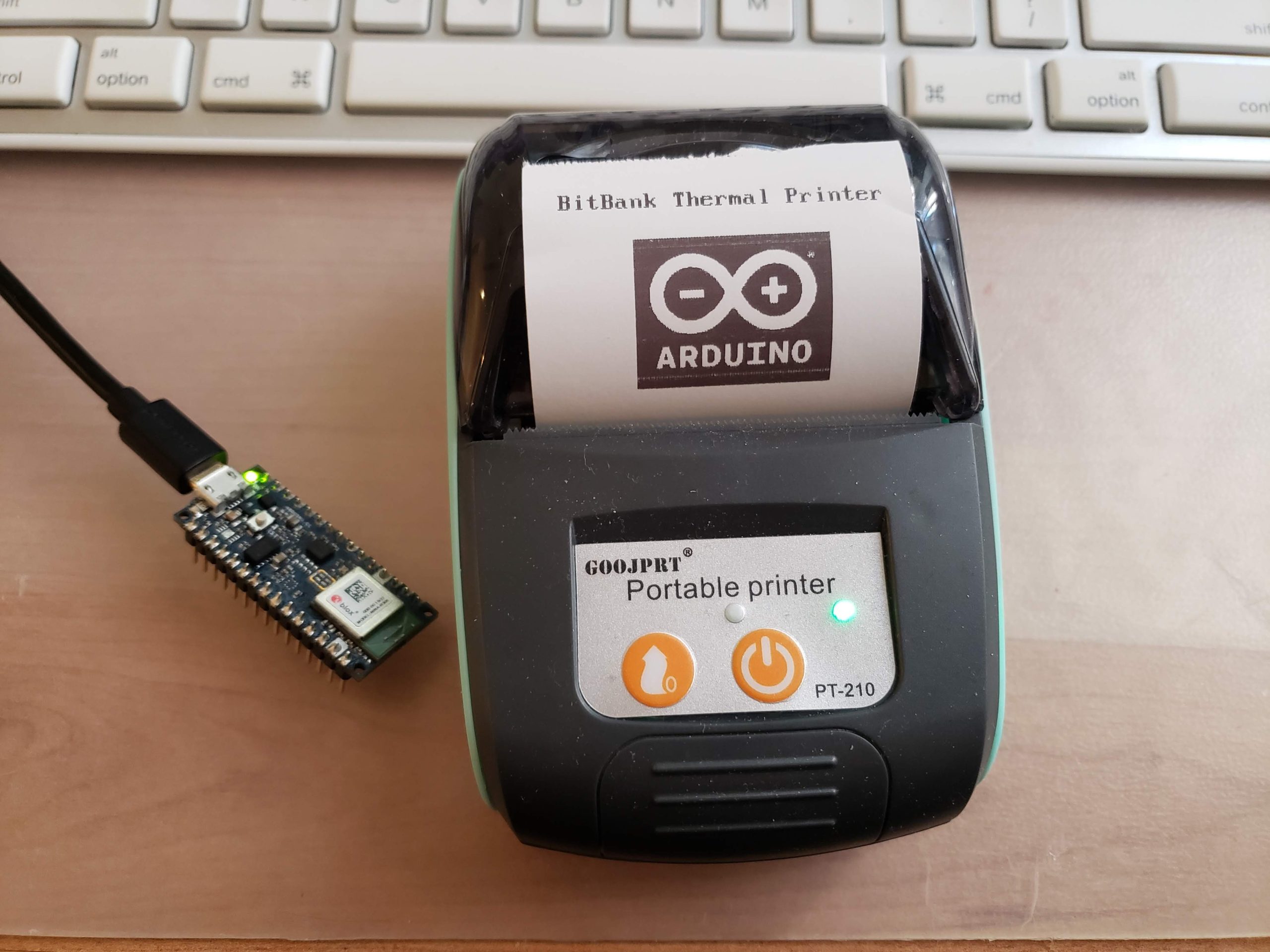
This Arduino library allows you to easily generate text and graphics and send them to a BLE thermal printer. Since there are many different BLE APIs depending on the board manufacturer, I decided to support the more popular ones – ESP32 and Arduino (Nano BLE 33). The two main features of thermal printers are supported by this code – plain text and dot addressable graphics. The graphics are treated as a display driver. You define a buffer and draw text, dots, lines, and bitmaps into it, then send it to the printer. Text output supports the various font size+attribute options of the printer. See the include (.H) file for a description of each function.
Features
Supports the GOOJPRT PT-210 printer (so far)
Compiles on both ESP32 and Arduino Nano 33 BLE
Supports graphics (dots, lines, text, bitmaps) and plain text output
Includes easy to use BLE scanning and connection logic
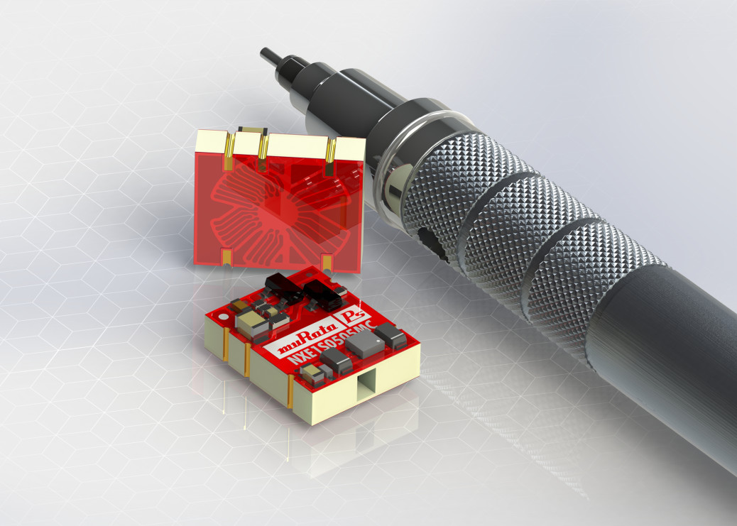
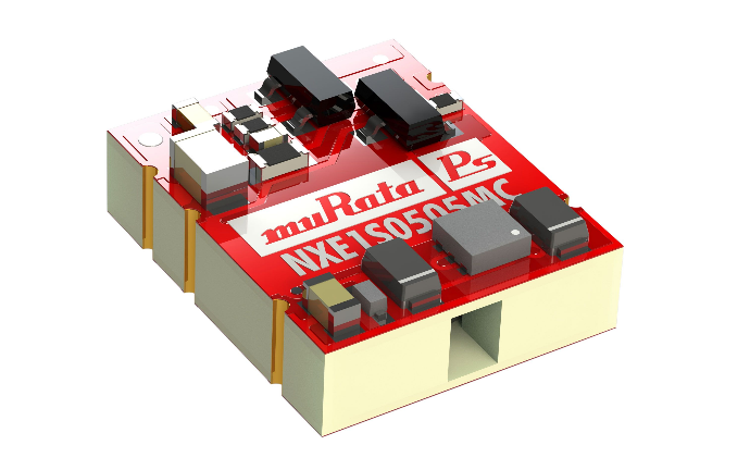
The NXE1 series is a new range of low cost, lower profile, fully automated manufacture surface mount DC-DC converters. The NXE1 series automated manufacturing process with substrate Embedded Transformer, offers increased product reliability and repeatability of performance in a halogen-free, iLGA inspectable package. The NXE1 series, industry-standard footprint is compatible with existing designs. The NXE1 series has a MSL rating 2, and is compatible with a peak reflow solder temperature of 245°C as per J-STD-020 and J-STD-075.
Teardown Video
The module is on sale for 2.7 EUR for single quantities. More information: power.murata.com
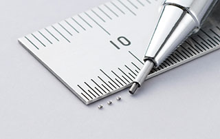
Murata has successfully commercialized the world’s smallestPTC thermistor (resettable fuse) with part number PRG03BC181QB6RL, in a 0201-inch size (0.6 x 0.3 x 0.3mm) package targeted for mobile devices. With an operating temperature from -20 deg C to 60 deg C the new PTC can provide excellent long term stability in high-temperature environments.
They has succeeded in commercializing the world’s smallest1 PTC thermistor2 (commonly known as a resettable fuse*3) in the 0201 inch size (0.6×0.3×0.3mm) for mobile devices, and has recently begun mass production of this device under the part number PRG03BC181QB6RL.
PRG03BC181QB6RL
As smartphones and mobile devices become increasingly multifunctional and more compact, demand is growing for smaller components that protect small electronic circuits and ensure device stability. PTC thermistors exhibit a rapid increase in electrical resistance when their temperature rises beyond a certain point, allowing them to protect circuits and components from damage. By identifying overcurrent in circuits that may occur during assembly or when a device is dropped or receives a sudden impact, PTC thermistors work to prevent abnormalities and failures in mobile devices.
Drawing on process technology originally developed by Murata based on its mainstay multilayer ceramic capacitors and multilayer devices, the PRG03BC181QB6RL has achieved an approx. 80% smaller volume and an approx. 70% smaller footprint than the company’s previous PTC thermistor (the 0402 inch size, 1.0×0.5×0.5mm). Built using Murata’s unique ceramic materials, the new product maintains its stable properties for a long time, thereby contributing to improving the safety of electronic devices.
Product highlights
The world’s smallest size (0201 inch, 0.6×0.3×0.3mm) ideal for multifunctional smartphones and small wearables
Murata’s own ceramic technology enables small resistance change and excellent long-term stability in high-temperature environments
Operating temperature range: -20°C to +60°C
NTC thermistors*4 have been used widely for controlling the temperature of electronic circuits in mobile devices. The new PTC thermistor will help manufacturers to prevent short circuits and further improve the safety of their products.
AC electric signals can be represented by three different methods in order to characterize and realize algebra operations with them. Already two methods have been presented in previous tutorials and a new graphical one is introduced later in this tutorial.
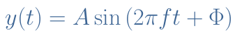
The most simple and natural way is to write an AC signal y(t) as a sine function of time such as explained in the tutorial of Sinusoidal Waveforms :
eq 1: Natural representation of an AC signal
With A being the amplitude, 2πf=ω being the angular velocity and f the frequency, Φ being the instant phase.
However, this representation is not convenient to realize algebra of two or more AC signals of the same frequency because there is no general trigonometric formula Asin(X)+Bsin(Y) to write a result under the form shown in Equation 1.
In the Complex Numbers tutorial, we have seen that y(t) can be rewritten as a complex number. This second way of writing a sine waveform simplifies the algebra between AC signals.
eq 2: Complex representation of an AC signal
Indeed, let’s consider for example that we want to add two signals y1(t) and y2(t), with their respective parameters A1, A2, Φ1, Φ2 and ω1=ω2. Using the complex form, the term ejωt can be put as a common factor :
eq 3: Addition of two complex AC signals
With A3 and Φ3 depending on A1, A2, Φ1, Φ2 being the new parameters amplitude and instant phase of the resulting signal y3(t).
In this tutorial, we will introduce a new representation of sine waveforms which is graphical and it is known as the phasor representation. The first section will present this new concept and clarify where it comes from.
At the core of the article, we will focus on the phasor’s algebra: how to realize additions/subtractions and differentiations/integrations. It will be highlighted why this representation makes the algebra of AC signals more convenient.
Presentation
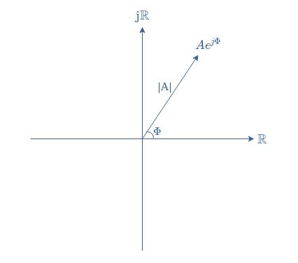
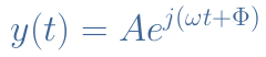
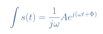
The idea of a phasor comes from the complex representation of AC signals. From Equation 2, we can indeed split the exponential term in two parts : Ae(jωt+Φ)=AejωtejΦ. We call phasor the quantity AejΦ, which is a complex number and can, therefore, be represented in the complex plane as a vector where Φ is the angle between the real numbers axis and phasor and A is the module of the vector :
fig 1: Representation of a phasor in the complex plane
Sometimes, AejωtejΦ can refer to the phasor, in this case, the vector rotates anticlockwise at an angular velocity of ω.
There is no real point in representing a single signal as a phasor, however, phasor diagrams become appreciated to solve some problems with two or more AC signals in an easier way than with algebra as we will present in the next section.
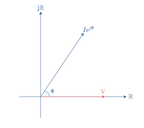
A phasor diagram consists of the same figure as presented above but with two or more vectors. Consider for example an AC signal which voltage and current are phase-shifted of Φ: V(t)=Vsin(ωt); I(t)=Isin(ωt+Φ). In this case, we represent V(t) as a reference phasor aligned with the real number axis and I(t) with an angle Φ oriented in the anticlockwise direction :
fig 2: Phasor diagram of two phase-shifted signals
In this particular case, the current is leading the voltage or we can also say that the voltage is lagging the current. More information about this fact can be found in the tutorial of Phase Splitter.
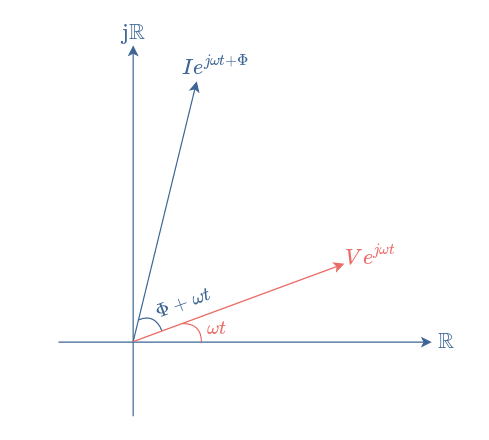
We note that since phasors represent the state of a signal at a particular period of time, an infinity of a diagram is available if we take t≠0. For this reason, the following diagram presented in Figure 3 is strictly similar to the one in Figure 2.
fig 3 : Phasor diagram at t≠0
However, we mostly prefer to draw the diagram such as presented in Figure 2 since it establishes a reference and because the angle ωt is not relevant.
One last comment before focusing on the phasor algebra would be to add those phasor diagrams that are only possible to draw when the signals are of the same frequency. The phase shift between two signals that are not synchronized isn’t constant and therefore the phasor diagrams at different times t1 and t2 would change.
Phasor algebra
Addition and subtraction
Phasor diagrams are very convenient when we need to add and subtract two signals that are not in phase.
When two signals are in phase, let’s say V1(t)=v1sin(ωt) and V2(t)=v2sin(ωt) it is indeed easy to addition them : V1(t)+V2(t)=(v1+v2)sin(ωt). However, when the signals are not in phase, this procedure does not work for the reasons mentioned in the introduction.
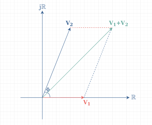
Consider two voltages signals of same frequency phase-shifted of Φ radians: V1(t)=v1sin(ωt) and V2(t)=v2sin(ωt+Φ). Figure 4 shows the procedure to add these two phasors :
fig 4: Addition of two phasors
Since the addition is a commutative operation, two ways of proceeding will lead to the same result: from V1 we add V2 (dashed blue line) or from V2 we add V1 (dashed red line).
If we consider the grid of Figure 4 to represent 1 V for each division, we can then determine the new amplitude and phase of V1+V2. We can see that V1+V2 can be written as a complex number of 5+5j. The amplitude of the output is, therefore √(52+52) = √50 ≈ 7 V and the phase is 45° or π/4 radians. Finally, we can say that V1+V2=7×sin(ωt+π/4).
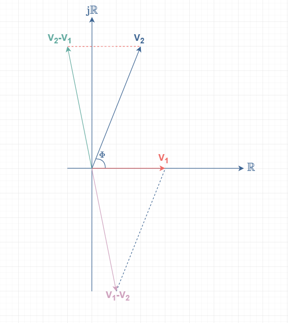
The procedure to subtract these two signals is the same, however, the subtraction is not commutative. This means that the result of V1-V2 or V2-V1 is different, as we are used to for real numbers :
fig 5: Subtraction of two phasors
The amplitude of V1-V2 or V2-V1 is identical and in our example would be equal to √(52+12) = √26 ≈ 5.1 V. The phase of V1-V2 is equal to atan(-5/1) ≈ -79° and the phase of V2-V1 is -79+180°=101°.
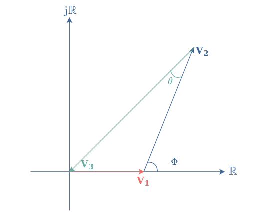
The phasor diagram is particularly helpful for some specific problems. Indeed, consider two signals of the same frequency V1 and V2 that are phase-shifted of an angle Φ, such as in Figure 4.
The problem is: which phase and amplitude are needed for a third signal V3 that results in destructive interference such as V1+V2+V3=0 ?
The phase diagram quickly and intuitively solves this problem :
fig 6 : A three signal destructive interference
Differentiation and integration
The differentiation or integration of phasors can help to solve differential equations related to first or second-order circuits.
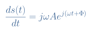
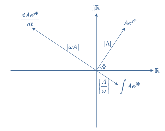
In order to understand how a differentiation or integration can be represented in a phase diagram, we start from the complex form and consider a phasor Aej(ωt+Φ).
The differentiation of s(t) is given by the expression in Equation 4 :
eq 4: Differentiation of a complex AC signal
The integration of s(t) is given by the expression in Equation 5 :
eq 5: Integration of a complex AC signal
The imaginary unit j can be rewritten ejπ/2, therefore the differentiation operation is similar to multiplying the phasor by ω and proceed to a rotation of +π/2 rad or +90°. The integration is similar to multiplying the phasor by 1/ω and proceed to a rotation of -π/2 rad or -90° such as illustrated in Figure 7 :
fig 7: Differentiated and integrated phasors in a phase diagram
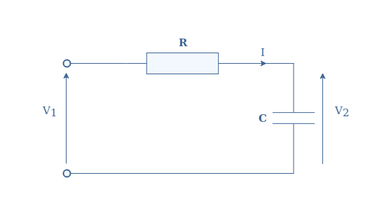
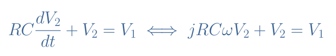
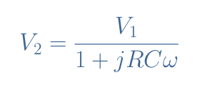
Consider an RC series circuit in which input voltage is the sine reference V1=v1ejωt and the output voltage is the unknown V2.
fig 8: RC series circuit
The voltages are linked by the following differential equation, which can be written in the classical form (left of the equivalence symbol) or with the phasor notation (right) thanks to the formula of derivation :
eq 6: Differential equation of an RC series circuit
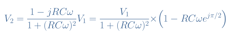
From this equation, we can express the unknown V2 as a function of the reference voltage :
Which can be rewritten by multiplying the numerator and denominator with the complex conjugate :
eq 7: Expression of the phasor V2
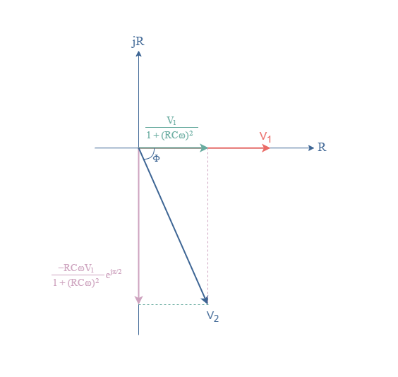
From this expression, we can represent the phasors of the RC circuit in a phase diagram in Figure 9 and proceed to the addition of two phasors in order to draw V2 :
fig 9: Representation of the input and output phasor of an RC series circuit
Both the amplitude and phase of V2 can be measured from this phase diagram with the same procedure that has previously been explained.
Conclusion
This tutorial has shown us a new method to represent and realize algebra on AC signals which is called phasors. A phasor can be both represented by a complex notation and also graphically in the complex plane as a vector which norm represents the amplitude and angle the phase of the signal.
When representing two or more signals in the same phase diagram, one of the signal always play the role of reference with a phase of 0°, aligned with the real number axis. The addition operation is commutative and can, therefore, be realized in two ways that lead to the same result. The subtraction is realized such as the addition but is not commutative.
Moreover, we have seen two other useful operations: differentiation and integration. In a phase diagram, the differentiation is equivalent to a positive rotation of 90° with multiplication by the frequency, the integration is equivalent to a negative rotation of 90° with a division by the frequency. These two operations are helpful in order to solve differential equations intervening in RC and LC circuits for example.
As the number of IoT devices increases, managing them all to keep online, secure, updated with the latest firmware, and remotely available, at all times, even when deployed behind firewalls and NATs, becomes quite the task. While quite a number of solution exists to some of these problems, they all usually have challenges like; the solution addressing just one or two problems or requiring technical know-how/skills (software or hardware) that could be expensive/scarce. To provide a holistic solution to this remote device management related problems, Norway-based qbee AS, launched its platform qbee.io.
The platform, which as a venture is backed by Innovation Norway and Simula Innovations, is designed to help users achieve four major things including; remote access, security, automation, and device monitoring.
For remote access, qbee.io allows connections over SSH but it can also map any other port such as web servers on 80/443 and Node-Red on 1880 or VNC. Out of the box, qbee routes all ports through a VPN connection using https on port 443. Its remote access features always draw a comparison with the TeamViewer IoT agent which doesn’t have some of the other features.
For Security, qbee performs actions like; check firmware libraries for CVE vulnerabilities, checks if newly updated libraries are available and make suggestions on upgrades, check which users are active and how old the passwords are (people tend to forget to remove pre-configured support accounts), rotate ssh keys, and close all incoming ports (ssh is routed through VPN). All of these actions and more are combined to ensure IoT deployments stay secure.
For device monitoring, qbee.io enables full configuration management through its state-based engine or via Ansible. It allows you to monitor device health by fetching metrics via log files, which could help you monitor issues like the device’s flash running out of space due to memory leaks or other performance-related problems. It also allows you easily update libraries and software and keeps an audit log so you know accessed the system or initiated a particular change.
Some of the highlight specifications and features of qbee include:
Enforce firewall security and update users or ssh keys.
Secure remote web server and remote desktop (VNC) access.
See current device metrics like CPU and memory use.
Software and package management
Monitor critical processes and respawn them.
Login access through a secure reverse tunnel
Configure services like Node-Red through templating.
Get logs and audit trails for any change or deviation.
Get alerts if devices go offline. Watchdog for the network stack.
Get visual feedback about device state and location.
One of the delightful things about qbee is its vendor-agnostic nature which allows it to work without the need for software development or containers. It works via the use of a lightweight, secure qbee agent packages which when on your IoT deployment, constantly monitors your system, receiving state information from the qbee backend server and autonomously enforcing the received data in the field. A flow chart showing how it works is provided in the image below.
The qbee agent packages currently exist for all Debian based systems and can be custom created for any other Linux based distribution. The absence of software development activities in qbee deployment makes it not just easy and fast to deploy, but also increases the range of devices(Legacy or new) on which it can be deployed.
Qbee offers value to everyone along the IoT development chain. It helps developers deploy without the time and resources required for software development, helps CIO/CISO keep an eye on security, and provides manufacturers a full IoT device management platform with remote access, security analysis, metrics and much more.
Qbee currently has 3 user plans including; “Small” which covers 1-25 devices at $4.30/month, “Medium” which covers 26-100 devices at $1.55/month, and “Large” which covers 101 – 250 devices at $0.90/month.
More information on qbee features, deployment, use cases, and pricing can be found on their website.
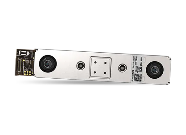
Intel® RealSense™ T261 Tracking Module is a tracking capable device that is based on the visual and inertial sensor fusion. This module uses dual fisheye cameras and Inertial Measurement Unit (IMU) for tracking features. The T261 module features processing from the Intel® Movidius™ Myriad™ 2 MA215x ASIC for 6 Degrees of Freedom (DoF) data streaming to the host system. This module is best suited for robots, drones, and augmented as well as virtual reality applications.
Features
Intel® Movidius™ Myriad™ VPU 2
High precision Visual Inertial Odometry Simultaneous Localization and Mapping (V‑SLAM) algorithms
6DoF data streaming to host
Low latency
OV9282 dual fisheye lenses with a combined with combined 163±5° FOV
BMI055 IMU for accurate measurement of rotation and acceleration
Picosun Group, global provider of leading AGILE ALD® (Atomic Layer Deposition) thin film coating solutions, reports record performance of silicon-integrated, three-dimensional deep trench microcapacitors manufactured using its ALD technology.
Increasing efficiency and performance demands of portable and wearable electronics, along with their shrinking size in accordance with the Moore’s law, set new challenges to the power management of these devices as well. A solution is further integration of the devices’ key components into so-called SiP (systems-in-package) or SoC (systems-on-chip) architectures, where everything, including the energy storage such as batteries or capacitors, is packed close to each other into one compact, microscale-miniaturized assembly. This calls for novel techniques to increase the performance and shrink the size of the energy storage unit as well. Three-dimensional, high aspect ratio and large surface area deep trench microcapacitors where ultra-thin, alternating layers of conducting and insulating materials form the energy storing structure, provide a potential solution.
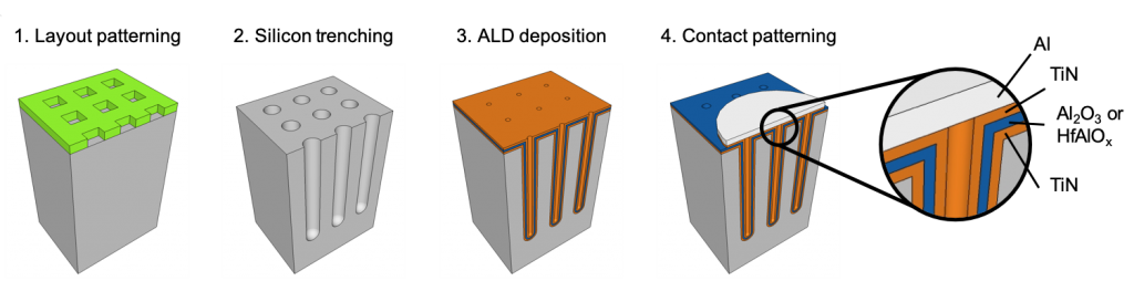
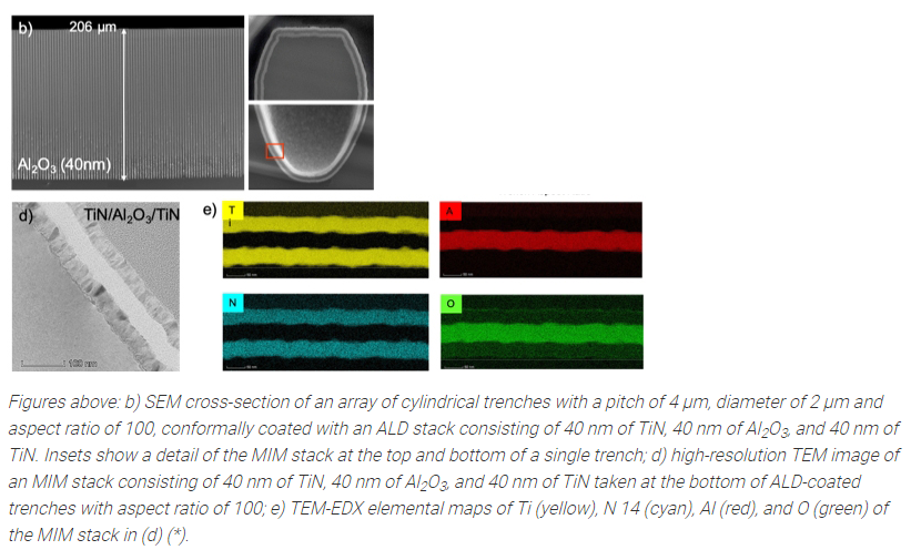
Picosun’s ALD technology has now realized unprecedented performance of these 3D microcapacitors. PICOSUN® ALD equipment were used to deposit film stacks of conductive TiN and insulating dielectric Al2O3 and HfAlO3 layers into high aspect ratio (up to 100) trenches etched into silicon. Up to 1 µF/mm2 areal capacitance was obtained, which is the new record for this capacitor type. Also power and energy densities, 566 W/cm2 and 1.7 µWh/cm2, were excellent and surpassing the values achieved with the most of the other capacitor technologies. The ALD microcapacitors showed also outstanding voltage and temperature stability, up to 16 V and 100 oC, over 100 hours continuous operation (*).
These excellent performance indicators pave the way to industrial applications of this capacitor technology. This is further facilitated by ALD’s mature position in modern semiconductor industries, where the technology is already integrated into practically all advanced microchip component manufacturing lines.
“We exploited the room available on the bottom of silicon wafers, of which only a few micrometers of silicon are used for electronic components in integrated circuits, to fabricate silicon-integrated 3D microcapacitors with unprecedented areal capacitance. The electrochemical micromachining technology, developed at the University of Pisa over the past decade, enabled etching of high density trenches with aspect ratios up to 100 in silicon, a value otherwise not achievable with deep reactive ion etching. This posed the basis for increasing the areal capacitance of our 3D microcapacitors upon conformal coating with an ALD metal-insulator-metal stack,” says Prof. Giuseppe Barillaro, group leader at the Information Engineering Department of the University of Pisa, Italy.
“The suberb results achieved with our 3D silicon-integrated microcapacitors show again how imperative ALD technology is to modern microelectronics. We are happy that we can offer our unmatched expertise and decades of cumulative know-how in the field to develop novel solutions for the challenges the industry is facing, when the requirements for system performance and integration level increase inversely to the system size. The environmental aspect is also obvious, when smaller, more compact devices manufactured in the same line mean also smaller consumption of materials and energy,” says Juhana Kostamo, deputy CEO of Picosun Group.
Picosun provides the most advanced ALD thin film coating technology to enable the industrial leap into the future, with turn-key production solutions and unmatched expertise in the field. Today, PICOSUN® ALD equipment are in daily manufacturing use in numerous major industries around the world. Picosun is based in Finland, with subsidiaries in Germany, North America, Singapore, Taiwan, China and Japan, offices in India and France, and a world-wide sales and support network. Visit www.picosun.com.