Particle accelerator fits on a chip

Researchers at Stanford University have demonstrated the acceleration of electrons through what they describe as an “On-chip integrated laser-driven particle accelerator”, detailed in a recent paper published in the Science journal. by Tom Abate

On a hillside above Stanford University, the SLAC National Accelerator Laboratory operates a scientific instrument nearly 2 miles long. In this giant accelerator, a stream of electrons flows through a vacuum pipe, as bursts of microwave radiation nudge the particles ever-faster forward until their velocity approaches the speed of light, creating a powerful beam that scientists from around the world use to probe the atomic and molecular structures of inorganic and biological materials.

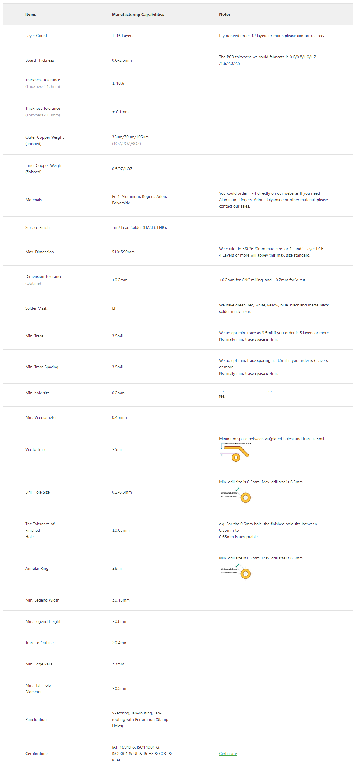
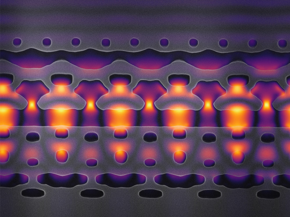
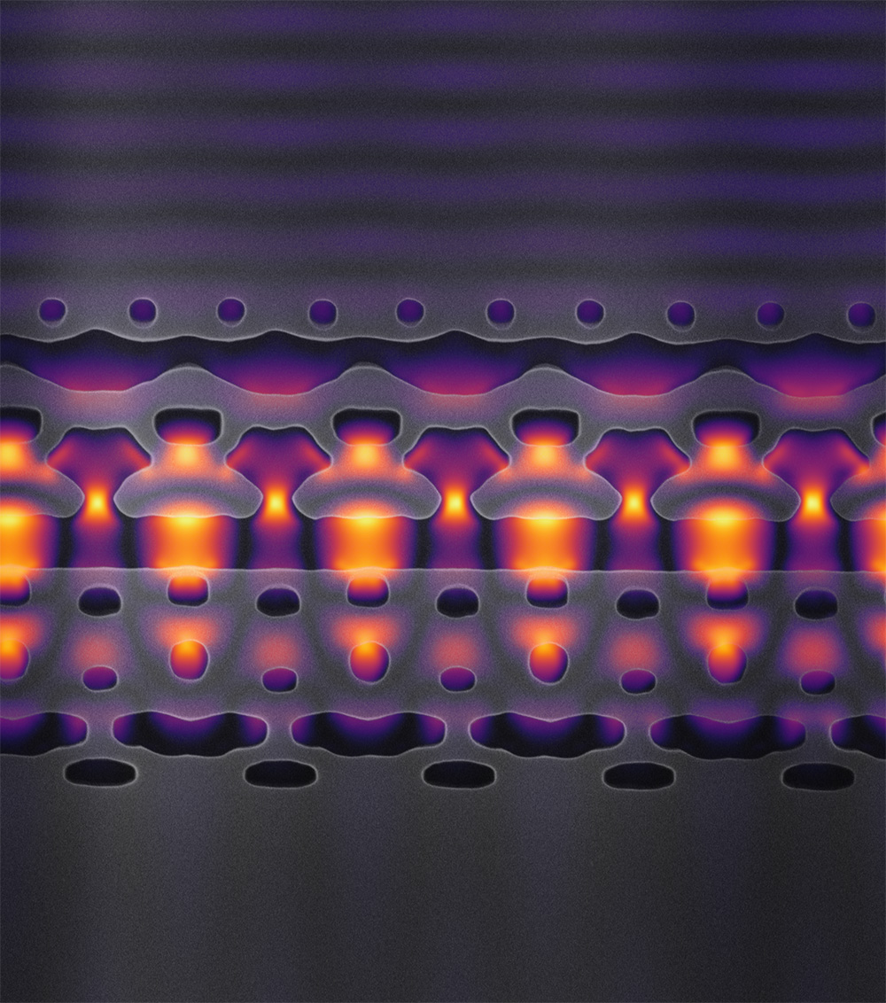
This image, magnified 25,000 times, shows a section of an accelerator-on-a-chip. The gray structures focus infrared laser light (shown in yellow and purple) on electrons flowing through the center channel. By packing 1,000 channels onto an inch-sized chip, Stanford researchers hope to accelerate electrons to 94 percent of the speed of light. (Image credit: Courtesy Neil Sapra)

Now, for the first time, scientists at Stanford and SLAC have created a silicon chip that can accelerate electrons – albeit at a fraction of the velocity of that massive instrument – using an infrared laser to deliver, in less than a hair’s width, the sort of energy boost that takes microwaves many feet.

Writing in the Jan. 3 issue of Science, a team led by electrical engineer Jelena Vuckovic explained how they carved a nanoscale channel out of silicon, sealed it in a vacuum and sent electrons through this cavity while pulses of infrared light – to which silicon is as transparent as glass is to visible light – were transmitted by the channel walls to speed the electrons along.

The accelerator-on-a-chip demonstrated in Science is just a prototype, but Vuckovic said its design and fabrication techniques can be scaled up to deliver particle beams accelerated enough to perform cutting-edge experiments in chemistry, materials science and biological discovery that don’t require the power of a massive accelerator.

“The largest accelerators are like powerful telescopes. There are only a few in the world and scientists must come to places like SLAC to use them,” Vuckovic said. “We want to miniaturize accelerator technology in a way that makes it a more accessible research tool.”

Team members liken their approach to the way that computing evolved from the mainframe to the smaller but still useful PC. Accelerator-on-a-chip technology could also lead to new cancer radiation therapies, said physicist Robert Byer, a co-author of the Science paper. Again, it’s a matter of size. Today, medical X-ray machines fill a room and deliver a beam of radiation that’s tough to focus on tumors, requiring patients to wear lead shields to minimize collateral damage.

“In this paper we begin to show how it might be possible to deliver electron beam radiation directly to a tumor, leaving healthy tissue unaffected,” said Byer, who leads the Accelerator on a Chip International Program, or ACHIP, a broader effort of which this current research is a part.

… continue reading

Remote Mail Notifier (and GPS Tracker)

published another great project. This time it’s a Remote Mail Notifier with GPS functionality. He writes:

At the moment I’m living in a block of flats and my mailbox is in a central lobby area. I’m often receiving small surprise packets from China and never know when the postman has been, usually between 8 and 12, sometimes even twice a day! I also don’t have any road facing windows that I can look out of for the bright red Royal Mail van.

So, I wanted to make something that can notify me of when the postman comes by and pops something into my mailbox. The previous place I lived at had the mailboxes at the far end of a gated car park, not great when it’s cold and wet!

I can’t have any cables going from the mailbox to my flat of course, so a wireless solution is needed. The first choice would have been to use WiFi, but the mailboxes are too far to get a signal to my back to my flat. I could probably use some kind of 433MHz radio module with a receiver in my flat, but I had recently come across A9G GPRS/GPS modules from A.I. Thinker that can have custom firmware loaded onto them. They only cost around £4 each, and it would also mean I don’t have to deal with annoying AT command parsing like with the popular SIM800. In the end I decided to go with the A9G and add secondary functions of being a listening bug and GPS tracker since it also has a built-in GPS receiver!

Remote Mail Notifier (and GPS Tracker) – [Link]

NextPCB.com Service Review

Printed Circuit boards are an important part of the development of any electronic product. They provide easy, neat, and repeatable ways of connecting components together. Thus, ensuring quality from their design to production is so critical that, failure at any point in the process could lead to a lot of money going to waste and delay in the project timeline, as such, the existence of several EDA software ensures the reliable design, the focus should then be on ensuring a manufacturer that is worth his weight in Gold, is selected for the manufacturing of the designs. One such manufacturer with experience and interesting capabilities is NextPCB and for today’s review, we will examine their processes, rates, and why you should probably choose (or not choose) them as PCB manufacturers for your next PCB project.

NextPCB is reputed as one of the most popular PCB manufacturers in China.  Situated at the heart of Shenzhen, NextPCB has been in the PCB manufacturing and assembly industry for over 15 years, providing some of the most innovative printed circuit boards, with assembly technologies of the highest quality standards, the fastest delivery turnaround (as fast as 24 hours), lowest manufacturer direct prices, and support via dedicated customer service professionals.

Using some of the latest machines and equipment, NextPCB provides two major services; PCB Manufacturing and PCB Assembly.

X-ray BGA Checking at NextPCB

Their PCB manufacturing services cover both PCB prototyping and Mass production with lead time as fast as 24hours and costs as low as 0$. They are capable of manufacturing up to 16 layers of PCB with a thickness of up to 2.5mm. All their PCBs are UL and ROHS certified which reduces the number of certifications the product companies need to go through.

A summary of the Key capabilities of NextPCB as regards printed circuit board manufacturing is provided in the table below. They created the table to help customers determine if the capabilities of the equipment being used by NextPCB match the requirements of their design, and to also serve as a tool to help NextPCB’s regular customers design their PCBs to match the capacity of the company.

For PCB Assembly, NextPCB provides a turnkey experience with services like;

  • Components/parts Sourcing
  • PCB Fabrication
  • Pick and Place Machine based board population
  • SMT & Through-hole assembly with wave soldering
  • 100% E-test and functional testing support
  • Worldwide free delivery with up to 30% off on the freight

A summary of some of the capabilities of NextPCB along the lines of PCB Assembly is provided in the table below;

For capabilities not listed in the table above, NextPCB works with the customer to ensure they are delivered.

NextPCB Quote form

To make access to these services easy, NextPCB has an online and instant PCB quote generator to which users can upload their Gerber files, and instantly get an evaluation of the design with a quote for its production. This makes it easy for developers to place orders for their boards from the comfort of their computers, and for situations that involve building a relationship with the company, NextPCB has a dedicated line through which customers can reach the company via their customer service professionals.

Functional Repair

NextPCB works to provide customers with reliable and flexible services, and one of the ways they do that is by providing customers with flexible payment and delivery options. NextPCB allows payment through channels like PayPal, Western Union, and ordinary bank transfer, while shipping and fulfillment are done via international logistics companies like DHL, FedEx, and the Singapore Post amongst others.

With an understanding of the big role the community plays, NextPCB is a big supporter of the open-source EDA community, supporting different community programs, and making donations to different community projects, including the widely popular KiCad for which NextPCB is regarded as one of the Main Sponsors.

NextPCB Drilling

Overall, compared with a number of PCB companies on the internet, the fact that NextPCB actually owns their factory (Not a Broker) and has been in the business for over 15 years means it will definitely be better to have them as partners for your projects, especially when for projects that require some level of experience in its manufacturing. Also, the parts sourcing services they provide help take a lot of burden off product companies as they will definitely have a wider reach and be able to help you get components that may be difficult to come by on the open market.

TPS7A24 – 8V tolerant, 2-µA IQ, 200-mA low-dropout (LDO) linear voltage regulator

The TPS7A24 low-dropout (LDO) linear voltage regulator supports a 2.4-V to 18-V input voltage range with ultra-low quiescent current (IQ). These features help modern appliances meet increasingly stringent energy requirements and help extend battery life in portable-power solutions.

The TPS7A24 is available in both fixed and adjustable versions. The fixed-voltage version eliminates external resistors and minimizes printed circuit board (PCB) area. For more flexibility or higher output voltages, the adjustable version uses feedback resistors to set the output voltage from 1.24 V to 17.75 V. Both versions have 2% output regulation accuracy that provides precision regulation for microcontroller (MCU) references.

TPS7A24 Internal Diagram

Features

  • Ultra-low IQ: 2.0 µA
  • Input voltage: 2.4 V to 18 V
  • Output voltage options available:
    • Fixed: 1.25 V to 5.5 V
    • Adjustable: 1.24 V to 17.75 V
  • 2% accuracy over temperature
  • Low dropout: 250 mV (max) at 200 mA
  • Active overshoot pulldown protection
  • Thermal shutdown and overcurrent protection
  • Operating junction temperature: –40°C to +125°C
  • Stable with 1-µF output capacitors
  • Package: 5-pin SOT-23

The TPS7A24 LDO operates more efficiently than standard linear regulators because the maximum dropout voltage is less than 250 mV at 200 mA of current. This maximum dropout voltage allows for 92.8% efficiency from a 3.55-V input voltage (VIN) to a 3.3-V output voltage (VOUT).

more information: www.ti.com

Google Announces New Coral products for 2020

Being one of the frontrunners in AI development and having an understanding of the potentials and opportunities in Edge Computing and Local AI, Google started its sojourn into the provision of hardware components and companion software tools for the development of Local AI products last year, with the launch of the Coral Platform.

The platform which comprises hardware components like the Coral Dev Board, the Coral USB Accelerator and PCIe accelerators was well received by the community with a diverse range of applications, across a broad set of industries already built on it. However, showing a strong desire to further grow the Coral ecosystem, Google, on Thursday, announced some of the new Coral products that will be released in 2020. The list included; The Coral Accelerator Module, the Coral Dev Board Mini, and a new Coral System-on-Module.

Coral Accelerator Module

The Coral Accelerator Module which was developed in partnership with Murata is an easy to integrate Multi-Chip package, power-efficient, and High-Speed on-board Edge TPU coprocessor, capable of performing 4 trillion operations (tera-operations) per second (TOPS), using 0.5 watts for each TOPS (2 TOPS per watt). The module exposes both PCIe and USB interfaces and can easily integrate into custom PCB designs without causing a significant increase in the board size due to its small form factor. The board supports TensorFlow Lite and AutoML Vision Edge, removing the need to build models from the ground up and facilitating the speedy deployment of high-accuracy custom image classification models.  According to Google, the Coral Accelerator Module will be available in the first half of 2020.

Coral Dev Board Mini

The Second Product billed for a 2020 arrival is the Coral Dev Board Mini, which according to Google will provide a smaller form-factor, lower-power, and lower-cost alternative to the Coral Dev Board. The Mini is said to be a combination of the new Coral Accelerator Module with the MediaTek 8167s SoC resulting in a board that excels at 720P video encoding/decoding and computer vision use cases. According to the announcement, the Coral Dev Board Mini will also be available in the first half of 2020.

Coral System-on-Module

Last but not least on the list is a new Coral System-on-Module. The new module is essentially a variation of the previous version and it comes with 2GB and 4GB LPDDR4 RAM in addition to the original 1GB LPDDR4 configuration. It retains all the other features including easy integration with custom hardware and support for TensorFlow lite and AutoML vision edge among others.

According to Google, all three products (and others under development) will be showcased at the CES 2020 in Las Vegas. The Coral Accelerator Module will be showcased at their booth at the Las Vegas Convention Center, Tech East, Central Plaza, CP-18, while the Coral Dev Mini will be at the MediaTek showcase located in the Venetian, Tech West, Level 3, and the new Coral SOM alongside several other new SOC and MCU explorations will be showcased at the NXP pavilion at the Las Vegas Convention Center, Tech East, Central Plaza, CP-18.

Meet the $795 USB 4.0 Switch for USB4 Product Development

A few months back, the specification for the USB 4.0 was released by the USB implementers forum with a promise of 2x the speed of USB3.2; 40GB/s and while there currently no devices in the market based on it, its features are definitely things device manufacturers will be leveraging on in a few months to increase their competitive advantage. This is why USB Solutions Provider, MCCI, recently announced the launch of their USB4 Switch which is targetted at helping developers and electronics companies fast track the development of their USB4-based devices.

According to MCCI’s product page, the new switch which is called the “3141 USB4™ Switch“, is a computer-controlled programmable 2:1 switch, connecting two USB Type-C™ receptacles to a single Type-C plug. It is compatible with USB4 hosts and devices, as well as older protocols such as Thunderbolt™ 3, USB 3.2, USB 2.0, USB Type-C Alternate Modes, and of course Power Delivery.

The Model 3141 USB4 Switch automates connect/disconnect of one or two devices to a USB Type-C port. It can be used in stress testing, switching between peripherals (for example, a dock and a display), or any automated reconfiguration of a USB Type-C port. It is compatible with the MCCI Model 3101 / Microsoft Type-C ConnEx Connection Exerciser tools and scripts and integrates with the tools in the Windows Hardware Lab Kit(HLK) to support participation in the Windows Hardware Compatibility Program.

Beyond formal compatibility testing of your final products, the Model 3141 has value throughout your product development cycle.  In our experience, long-run randomized switching on a USB Type-C port is highly effective in exposing bugs in the hardware-firmware-software stack on both hosts and devices. Developers can use it with a simple UI on the control computer to connect/reconnect a device under test without physically manipulating cables, reducing wear on fragile prototypes. Continuous integration systems can use it to reproducibly test key scenarios of devices under test with a variety of test setups.

Some of the features of the switch include:

  • Supports USB4, Thunderbolt 3, USB 3.2 gen2 (x2 and x1), gen 1 (x2 and x1), USB 2.0 high speed, full speed, and low speed, USB Power Delivery, VCONN-powered devices (up to 0.5A), and alternate modes like DisplayPort™.
  • A transparent connection between SUT and DUT when in the connected state.
  • Impedance controlled low loss USB data path.
  • USB4/Superspeed signals are switched by Diodes PI3DBS16212 20Gbps 1-Lane, 2:1 Mux switches
  • Uses TI TUSB221 1:2 High-Speed USB Multiplexer/Switch for USB2.0 signals.
  • Uses Maxim Integrated’s MAX14589E analog switches for CC lines and SBU signals
  • Handles up to 20V and 5A on VBUS
  • Includes AVR 32U4 CPU, with open-source Arduino BSP and firmware.>
  • Controlled and powered via USB micro B connector. Standard firmware uses CDC ACM virtual serial port for remote control.
  • Indication lights for connection indication, and for cable orientation on receptacles (normal or flipped).
  • Tiny form-factor (1.6” by 1.6” / 31mm by 31mm), fully enclosed for safe handling.

Limitations

In order to keep the 3141 simple and effective for a variety of applications, a few features were specifically omitted. Contact MCCI if you need more information.

  • The 3141 handles VCONN powered devices drawing up to 0.5 A of power. Higher power devices are not supported.
  • The 3141 does not support automatic Type-C cable flipping.
  • For maximum signal integrity, USB 2.0 lines are available only at A6/A7 pins of the Type-C plug. Some systems connect A6/A7 to B6/B7 as shown in figures 4-3 and 4-4 of the USB Type-C specification, and operate without restriction. Other systems do not connect A6/A7 to B6/B7, and require data orientation to follow CC1 orientation. When working with such systems, you must correctly insert devices into the 3141 Type-C receptacles.  The cables/devices must be plugged in with A6/A7 matching 3141 A6/A7 (not flipped, with A6/A7 matching B6/B7). Indicator lights clearly show the operator when the cables are connected in the direct (not flipped) orientation, and the test control computer can also detect the orientation.

Software requirements

When running Microsoft Windows HLK test scripts, the Model 3141 USB Switch is controlled over the micro-USB port by a test control computer running Windows and the Microsoft MUTT ConnEx-C software package. This software may be obtained from Microsoft via the “Tools in the MUTT Software Package” page.

The Microsoft software package includes utilities to update the firmware, switch between the peripheral ports, and send requests to simulate test cases.

MCCI also supports other test scenarios using a USB test control system, with software available from MCCI, or with customer-written software.

MCCI supplies a full Arduino BSP and can support customer-developed software, or can provide firmware customized to meet customer requirements.

Direct control

It’s easy to use the 3141 to implement custom test scenarios for non-Windows platforms, or to test embedded devices. The control port is a standard CDC ACM device, and so will show up as a virtual COM port on most standard operating systems. Commands are easy-to-remember high-level commands.

Custom Variants

Special variants of the 3141 are available by request. Please write sales@mcci.com with your requirements.

Price and Availability

The Model 3141 is available now. Current pricing may be found on MCCI’s online store, https://mcci.io/buy-USB4Switch. For more information, please contact MCCI at sales@mcci.com, Twitter @MCCIhttps://mcci.com.

Building an extremely high powered 1-12V lab power supply on the cheap

Matthew Millman has published a new project:

For a number of years now I’ve had a couple of high powered switching power supply units made by Power-One. They’re typically found in I.T. equipment and provide a single output rail of either 12 V or 48 V with a very high current rating. The other cool thing is that in the case of the 12 V model – the output voltage can be changed in software from 1 V to 12 V (12.45 V is the max). The 48 V model does not allow configuration of the output voltage frustratingly.

Building an extremely high powered 1-12V lab power supply on the cheap – [Link]

Seeeduino Crypto Board features ATmega4809 & ECC608

As the name indicates, this board is born for encryption. Seeeduino Crypto is based on high-performance ATmega4809 and featured with Microchip ECC608 crypto chip. With the help of the ECC608 crypto chip, you can experience encrypted communication, such as I2C encryption.

Along with the encryption, Seeeduino Crypto is functionally the same as the Seeeduino V4.2 / Arduino Uno Rev3. It has wealth interface resources, including 6 analog input pins, 14 digital I/O – 5 of which can work as PWM output, not to mention, as part of the Seeeduino family Seeeduino Crypto comes with 2 Grove I2C port and 1 Grove UART Port. Now the whole Grove system is yours, you can play with hundreds of sensors and actuators simply by plugging.

The control solution Seeeduino Crypto is the same as ARDUINO UNO WIFI REV2. The difference is that Seeeduino Crypto does not have onboard WIFI. You can add an Arduino wifi module if necessary. Correspondingly, the price of Seeeduino Crypto is less than half of ARDUINO UNO WIFI REV2.

Features

  • High-performance ATmega4809 microcontroller
  • High-securitycryptographic Chip ECC608, supports SHA-256 & HMAC Hash / AES-128
  • 2 Grove I2C + 1 Grove UART, easy to prototype
  • Type C power supply + data transmit

Specifications

The board is on sale on Seeestudio for $19.90 USD from the CN warehouse.

Torex & NGK Partner on Power Module Reference Design for IoT Devices

Torex Semiconductor Co., Ltd. and NGK Corporation will exhibit a compact power module sample that can be processed through high-temperature surface mount with using Torex power management ICs and NGK EnerCera series batteries at CES 2020 (January 7th to 10th, 2020 at Las Vegas in the USA). [via]

By combining the characteristics of NGK EnerCera batteries which include high capacity with low resistance and surface mounting, with high-temperature reflow process and the characteristics of Torex power management IC’s which are ultra-low power consumption and ultra-small and thin packages, the companies realized a very small space for the battery and charging control circuit including the power management ICs.

The resulting reference design is optimal for IoT devices and smart cards. The companies will exhibit this module sample in the Torex and NGK booths at CES 2020.

About EnerCera Li-ion Batteries

EnerCera is a Li-ion secondary battery with NGK’s original Crystal Oriented Ceramic Plate as electrodes. The Crystal Oriented Ceramic Plate is composed of just an active material and it contains no organic binder or conductive material that exists in a Li-ion battery normally but does not contribute to battery capacity.

As a result, EnerCera realizes high energy density and low internal resistance with a small and thin body and is capable of high-temperature installation. The energy density is double and the internal resistance is less than a half compared to commercial secondary batteries of the same size.

Therefore, EnerCera is an ultra-small/ultra-thin onboard-type high-performance battery for operating ICs, sensors and a wireless communication system that needs large current such as several 10mA to several 100 mA.

In addition, CV (Constant Voltage)-charging capability eliminates the need for a charger IC to control the charge current.

more information:NGK Insulators Ltd. , Torex Semiconductor

300W GaN-Based Ultra-High Power Density AC-DC Adapter Reference Design

GaN Systems and ON Semiconductor announced the availability of the NCP13992UHD300WGEVB, the world’s highest power density 300W ac-dc adapter reference design using GaN Systems’ 650V, 15A gallium-nitride (GaN) E-HEMTs and multiple ON Semiconductor controller and driver ICs, including the NCP51820, NCP13992, NCP1616, and NCP4306.

This complete system reference design is a highly versatile and low cost, allowing designers to easily develop and bring to market ultra-high power density (UHPD) ac-dc adapters for various applications in HDTV power supplies, gaming notebook, and console adapters as well as ultra-small power supplies for industrial and medical devices.

This ac-dc adapter reference design is based on a modular concept that brings several advantages including; versatility, the possibility to test own daughter cards, easy design update, the opportunity for checking functionality separated module, and spare room for additional features. These allow the user to enhance experimenting with daughter cards.

This modular construction also helps to reduce PCB area, thus increasing power density and also allowing for a reduced number of PCB layers. All PCBs are designed as 2−layers with 70μm copper plating for better thermal management. Also, the 70μm copper helps to reduce conduction losses especially on the secondary side which carries relatively high output current.

Assembly steps of the modular NCP13992UHD300WGEVB reference design.

Summary of Features

  • GaN HEMT Based Design with Ultra−High Power Density Up to 32 W/inch3
  • Simple Two Layer PCB Design for all Board Modules
  • 300W Maximum Power with Peak Power Up to 340W at Fixed Output Voltage 19V
  • Wide Input Voltage Range 90- to 265-Vrms
  • Synchronous CrM PFC with using GaN HEMT
  • 500kHz LLC Stage Incorporated with 600V HV GaN Driver and High Performance Current Mode LLC Controller
  • Complies with CoC5 Tier2

This reference design/evaluation board demonstrates ON Semiconductor’s high-performance controllers, drivers and discrete semiconductor content capabilities that enable efficient UHPD design implementation. This design includes a synchronous power factor correction boost converter which is operated in the discontinuous conduction or critical conduction mode (DCM/ CrM) depending on loading and LLC power stage, with secondary-side synchronous rectification.

The PFC front stage is driven by NCP1616 controller, which assures unity power factor and low input current THD. Synchronization of the PFC boost SR switch is enabled by the NCP4306 high-performance SR controller.

The LLC stage operates at 500kHz switching frequency while the nominal load is applied. The power stage is managed by the NCP13992 high-performance current mode LLC controller. Thanks to the GaN HEMTs implemented in both power stages at the primary side, the high efficiency is easily maintained despite the fact that the system operates at high frequency. GaN Systems’ GS66504B are incorporated as primary side power switches.

The synchronous rectifier (SR) stage used in the secondary side includes the NCP4306 and two paralleled 60V power MOSFETs for each branch. The synchronous rectification MOSFETs and controllers are implemented on the dedicated daughter card to ease the main power board PCB design and to achieve maximum efficiency.

Ultra-high power density is achieved thanks to the modular design, and the combination of controllers / drivers, GaN HEMTs, and the dedicated power magnetics design. The resulting GaN-based adapter provides a highly cost-effective solution.

“Fast-switching GaN works effectively with our advanced controller and drivers to optimize system designs for high power density, removing design barriers and enabling designers to take advantage of the numerous benefits provided by GaN E-HEMTs,” stated Ryan Zahn, Director of Marketing at ON Semiconductor.

“With rising interest and adoption of GaN, we look forward to continued collaboration with GaN Systems to support and meet the new power requirements taking place across many industries.”

“Our collaboration combines ON Semiconductors’ system applications expertise and industry-leading power IC products with the world’s most advanced 650V GaN E-HEMTs. This reference design developed in collaboration with ON Semiconductor makes it easier and more cost effective to design as GaN gains popularity as a building block in the adapter market,” said Charles Bailley, Senior Director, Worldwide Business Development at GaN Systems. “This release is the first of several systems and integrated packaging innovations in development, which will significantly expand the GaN ecosystem.”

more information: www.onsemi.com

TOP PCB Companies