The i.MX RT Family Makes for Some Feature Filled Feathers!

Thanks to a host of useful feather wings and shields, the Adafruit Feather form factor is becoming a very popular one with a host of other boards now based on it, offering not only the shape and size but also pin compatibility to allow the use feather addons like the FeatherWings and shields. In line with this, Arturo (@Arturo182) recently announced via his twitter handle that he is working on two new Feather form-factor development boards which are based on NXP’s i.MX RT Family of microcontrollers.

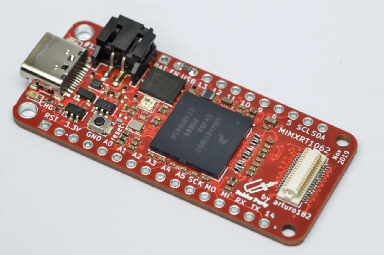
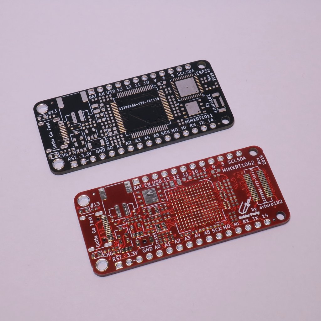
The first board, which is based on the RT1062 MCU is loaded with almost the same functionalities you will find on the Teensy 4.0. It comes with the feather standard arrangement of I/O headers with an extra expansion header that breaks out a suite of pins to allow access to the awesome display interface available on the RT1062. The breakout pin’s to the display interface, which is capable of driving WXGA panels which have a resolution 1366 x 768 pixels and it is also available for use as extra GPIOs when using the board without a display.

Unpopulated Feather Boards

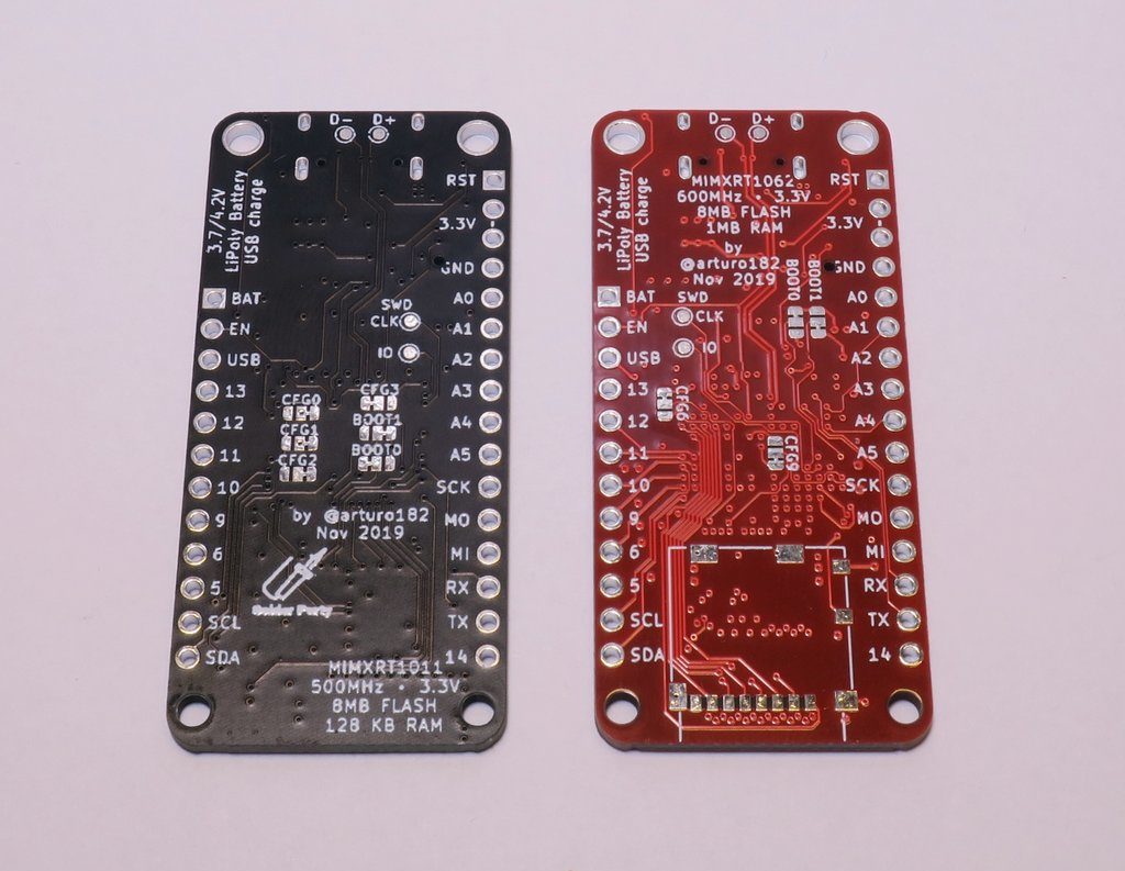
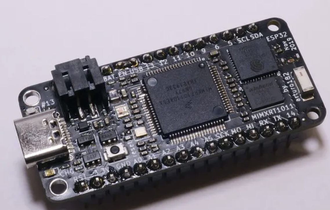
The second board is, quite the kicker as it implements not just the RT1011 microcontroller, but also the popular ESP32 module. Coming in a black PCB color, the board trades in extra I/O pins for a hand-solderable QFP package, with the ESP32, complete with all RF components, connected in place of the display extension header on the RT1062 based board. Rather than using the ESP32 in its full glory, which I am sure the component itself would maybe have preferred, it is being used as a WiFi Co-processor, providing WiFi connectivity features to the board while leaving the more powerful RT1011 to focus on running the Circuitpython stack and other burdens laid on it.

RT1011 + ESP32

Both boards contain pretty tightly packed features but a summary of highlight features, common to both boards, include:

  • Adafruit Feather Form-Factor and Pin Compatibility
  • NXP i.MX RT series processor on both boards
  • USB-C connection (with USB2.0 Specifications) for power and data/programming.
  • Both boards support circuit python
  • Battery charging for Lithium-Ion cells, via an onboard 2.0mm JST connector

While the boards are still under development, following the twitter thread shows that he has overcome some of the major challenges with the boards and should be rounding them up very soon. The thread also shows several ingenious approaches as for instance, both boards Leverage on the recent inclusion of RT MCU series support in tinyUSB to provide REPL access over UART.

Arturo has created some amazing boards like the SAM D21 based board called “Serpentine” in the past and based on his track records, we should be seeing these boards on his Tindie page very soon.

Meet the STM32 “Black Pill” Development Board

After playing second (maybe third?) fiddle for a while to a range of maker-friendly boards from Arduino and others, STMicro finally got it right with the STM32F103C8T6 Arm Cortex-M3 microcontroller-based “BluePill” development board which can be programmed using the Arduino IDE. As all good hardware requires, a new version of the board which is being called the “Blue Pill 2” or “Black Pill” was recently released.

The new board which is already widely available on platforms like Aliexpress, seems to be based on a diverse range of STM32 microcontrollers including the F1 and F3 series. However, the one we found to be most interesting was based on the Arm Cortex-M4 F401 series, which according to one of the Aliexpress vendors, is cheaper than some of the microcontrollers in the F1- Series.

Asides the cost, the F401 series of microcontrollers were also found to be better than the F1 in terms of frequency and also come with a floating-point arithmetic module, and an IO port that contains all the basic functions. In terms of the specific  F4 microcontroller used, most of the boards on sale currently were found to come with the STM32F401CCU6 or the STM32F411CEU6 microcontroller.  The STM32F401CCU6 version of the board clocks in at 84 MHz with a 256 KB  flash, and 64KB of SRAM, while the STM32F411CEU6 clocks in at 100 MHz with a 512KB flash, 128KB of SRAM. The Black Pill also allows you to add additional flash by soldering an SPI Flash to the board.

STM32F401 Development Board

The board also follows the pivot away from micro USB by recent development boards as it comes with a USB-C port through which programming is done. Talking about programming, the board could be programmed using the Arduino-C via the Arduino IDE and Micropython. The Arduino Board support files can be downloaded via the Arduino Board Manager, while the Micropython Firmware for the board can be obtained from the suppliers on Aliexpress.

All-in-All, the Black Pill retains the same form factor as the blue pill with dimensions of 5.3cm x 2.2cm and similar pin-outs for the 2×20 GPIO pins some of which carry I2C, SPI, ADC capabilities.

The board is available from different sellers on Banggood and Aliexpress for a price of around $3 and more information on it can be obtained from their product page.

ATL431LI High-Bandwidth, Low IQ Programmable Shunt Regulator

Texas Instruments’ regulator features active output circuitry making it an excellent Zener diode replacement in many applications.

Texas Instruments’ ATL431LI device is a three-terminal adjustable shunt regulator with specified thermal stability over applicable automotive, commercial, and military temperature ranges. The output voltage can be set to any value between VREF (approximately 2.5 V) and 36 V, with two external resistors. This regulator has a typical output impedance of 0.3 Ω. Active output circuitry provides an ultra-sharp turn-on characteristic, making these devices excellent replacements for Zener diodes in many applications such as onboard regulation, adjustable power supplies, and switching power supplies. This device is a pin-to-pin alternative to the TL431LI and TL432LI, with a lower minimum operating current to help reduce system power consumption. The ATL432LI and the ATL431LI have the same functionality and electrical specifications, except the ATL432LI has a different pinout for the DBZ package. The ATL431LI is offered in a tiny X2SON (1.00 mm x 1.00 mm) package which makes it ideal for space-constraint applications.

The ATL431LI device is offered in B grade and A grade with initial tolerances of 0.5% and 1% (at +25°C), respectively. The low output drift versus temperature ensures good stability over the entire temperature range. The ATL43xLIxQ devices are characterized for the operating temperature range of -40°C to +125°C.

Features

  • Reference voltage tolerance at +25°C:B grade: 0.5%, A grade: 1%
  • Output voltage: 2.5 V (minimum typ.), VREF to 36 V (adjustable)
  • Operating temperature range: -40°C to +125°C (Q temp)
  • Max temperature drift: 17 mV (I temp), 27 mV (Q temp)
  • Output impedance: 0.3 Ω (typ.)
  • Sink-current capability: Imin: 0.08 mA (max.), IKA: 15 mA (max.)
  • Reference input current IREF: 0.4 µA (max.)
  • Deviation of reference input current overtemperature, II(dev): 0.3 µA (max.)
  • Packages: 1 mm x 1 mm X2SON or SOT23-3

more information: www.ti.com

InspectAR constantly improves and recognizes your PCB

Augmented and Virtual Reality rank among the top 10 technologies driving Industry 4.0 and while they are having a huge impact on the development of new devices, it’s interesting to see them also being used as a major ingredient in the technology development process. This was one of the reasons why a while back we took a look at InspectAR which is an augmented reality-based app that is currently disrupting how developers and users interact with printed circuit boards.

In the last article, we mentioned how the InspectAR app uses augmented reality to lay a similitude of your board’s design over a real-time image of the actual physical board. The overlayed similitude is obtained from your PCB’s original Gerber files, so you can toggle which layers are visible at any given time with an additional exploded view feature that allows you view multiple/all layers at once. As you move the board, the overlayed similitude layer automatically moves and changes orientation and view in line with the physical PCB, giving you the ability to inspect the design at any angle. For example, by simply turning on a trace layer, users can see if a pin is properly connected to a component or if you made a mistake during the design phase — or the manufacturer made a mistake during fabrication.

The SuperCon Badge

However, thanks to constant efforts going into the software, the team has made several upgrades since then. Some of those updates were displayed by the team during the last SuperCon Conference by Hackaday. As a way of demonstrating the new features, the InspectAR team preloaded the FPGA based SuperCon badge into InspectAR. This allowed users to get detailed information about the badge’s hardware using the InspectAR App. When users point their cameras to the badge, InspectAR displays overlays on the badge, via the screen. The overlays display information like pin numbers, PCB traces and part numbers of the components on the board. This reduced the need for users to look up the datasheet or Pinout of components every now and then.

The overlays displayed by the App are usually in layers, as such, to ensure things are neat and useful, the app provides a way for users to hide and switch between the layers. Also, the annotations displayed on each component/part of the PCB can also be moved such that it is positioned in a place the user finds comfortable.

While it’s still early days, the amount of work going into InspectAR makes it easy to predict a bright future for the project. There is every chance that InspectAR and other software like Circuit-Tree will grow into becoming tools that define how design is done in the future.

More on how InspectAR works can be found on their website and Blog.

Waveshare releases a Compute Module IO Board with POE Feature

As the Raspberry Pi grew popular, users began to ask for a more flexible form factor which will allow the use of the Raspberry Pi capacities in products, especially those with industrial applications. The response of the Raspberry Pi’s team to these demands was the Raspberry Pi Compute Module which, now is in its third version, carrying the Raspberry Pi’s gut from Processor to RAM. Since the Compute Module was a bare-bones board with none of the IO and Ports that makes prototyping easy with the Pi, the Raspberry Pi Foundation decided to create an accompanying board called the Compute Module IO Board, which is capable of providing the IO, ports and other features that make the compute module easy to use and program like the normal Raspberry Pi. The design of the compute module was made open source and since then, several manufacturers have made their own IO boards with different improvements to make it more useful. One such board is the recently released POE Enabled, Compute Module IO Board by Waveshare.

Compute Module IO
Compute Module IO


The Compute Module PoE Board is a development board that you can plug a Raspberry Pi Compute Module into, and make use of the resources of Pi more flexibly. With the PoE (Power over Ethernet) feature, and versatile onboard peripheral interfaces, it is suitable for evaluating the Raspberry Pi compute module, also is an ideal choice for end products. The board comes with a Camera interface, USB ports, HDMI Ports, and GPIO headers that allows users to connect sensors to the Compute module. Courtesy of the Power Over Ethernet feature of the board, the board can be powered over the ethernet port. This reduces the number of cables needed in case of large deployment as the same ethernet cables used for network connectivity also powers the system.

Some of the features of the board are highlighted below:

  • Raspberry Pi GPIO header, for connecting sorts of Raspberry Pi HATs
  • 10/100M auto-negotiation Ethernet port, with PoE, enabled
  • 4x USB ports allow connecting more USB devices
  • 2x CSI camera interfaces
  • Onboard HDMI / DSI interfaces for connecting displays
  • Onboard USB TO UART, for serial debugging
  • Cooling fan interface, autorun on power-up OR controlled by IO pins
  • Adopts isolated SMPS (Switching Mode Power Supply)
  • Power supply over a micro USB port  or the Ethernet port
  • 37V ~ 57V DC Input power
  • 5V 2.5A DC output Power
  • 802.3af PoE standard
  •  Board dimension 114mm × 84.4mm

Although it’s sold as a separate entity, a plastic enclosure called the CM-IO_POE Box exists for the IO board. The enclosure has a vent, presumably for a Fan, along with other features to support the IO board.

Waveshare created a Wiki page which provides enough information to help first-time users get up and running with the board in a couple of minutes. The board is available on Seeedstudio for $40 and on the Waveshare store page for $38

COM-WHUC6: Industrial Power on Module from AAEON

AAEON, an industry leader in embedded computing, announces the COM-WHUC6 COM Express module. Built to the Compact Type 6 form factor, the COM-WHUC6 is designed to operate in a range of applications from automation to mobile operations.

The COM-WHUC6 is powered by the 8th Generation Intel® Core™ i7/i5/i3 and Celeron® ULT series processors (formerly Whiskey Lake), providing energy efficient performance for a range of industrial and embedded applications. Coupled with two DDR4 slots and up to 64GB of on-board eMMC storage, the COM-WHUC6 is designed to provide optimized processing capabilities.

Built for industrial embedded use, the COM-WHUC6 is designed with several key features to ensure flexibility and ease of maintenance. I/O support for USB 3.2 Gen 2 provides high speed connectivity, and support for VGA, eDP/LVDS, and DDI makes it easy to fit into existing setups. The COM-WHUC6 supports expansion for two SATA III devices and five PCIe devices.

The COM-WHUC6 is backed with AAEON support and can be easily configured to a range of options, including WiTAS 2 compliance for operation in temperatures from -40°C to 85°C. With AAEON manufacturer services and OEM/ODM support, AAEON can easily provide COM carrier boards, custom I/O and PCIe support configurations, and more.

The COM-WHUC6 can support a wide range of embedded applications, from automated inspection to mobile medical devices. The Compact Type 6 form factor means the COM-WHUC6 is easy to install, replace, or even upgrade when the time comes. The COM-WHUC6 also supports applications requiring multi-module configurations.

“The COM-WHUC6 is a highly versatile COM module,” said David Hung, Product Manager with AAEON’s Embedded Computing Division. “With the 8th Generation Intel® Core™ and Celeron® processors along with its wide temperature design, the COM-WHUC6 can be deployed anywhere for any task.”

for more information visit www.aaeon.com

Intel® NUC 8 Rugged PC

Intel® NUC 8 Rugged is a PC kit that’s small on size but not on toughness or reliability. It features a fanless, ventless design to minimize particle intrusion, so it’s built to survive environments most PCs can’t—from a busy factory floor to a dusty warehouse. And even without a fan, it can operate in temperatures from 0-40˚C to thrive in severe in-the-field conditions.

Housed in a small chassis that’s slim enough to fit almost anywhere, the NUC 8 Rugged is also available as a board-only option that can be easily integrated into your own digital solutions. It’s powered by an Intel® Celeron® processor, making it the ideal PC solution to keep edge analytics, digital signage, or surveillance cameras up and running around the clock. And with a 3-year warranty, it’s performance that’s designed to last.

Features

  • Intel® Celeron® processor
  • Fanless and ventless design
  • Minimal dust intrusion
  • Qualified for 24×7 operation
  • Multiple mounting options
  • Dual HDMI*
  • 2 USB 3.0 ports
  • 2 USB 2.0 ports
  • Internal 4-lane eDP connector
  • Intel® Wireless-AC
  • Bluetooth® technology
  • Intel® Gigabit LAN
  • 3-Year limited warranty

-> Product Brief PDF

MLX90374 Position Sensor

Melexis’ MLX90374 monolithic magnetic position processor IC enables the design of non-contacting position sensors in automotive and industrial applications

Melexis’ MLX90374, a Triaxis® family position sensor, offers stray field robustness featuring two output drivers, high operating voltage, and temperature operation.

The MLX90374 is a monolithic magnetic position processor IC. It consists of a Triaxis Hall magnetic front end, an analog-to-digital signal conditioner, a DSP for advanced signal processing, and a dual output stage driver.

The MLX90374 is sensitive to the three components of the magnetic flux density applied to the IC (i.e., Bx, By, and Bz). This allows the MLX90374 with the correct magnetic circuit to decode the absolute position of any moving magnet (e.g., rotary position from 0 to 360° or linear displacement). It enables the design of non-contacting position sensors that are frequently required for both automotive and industrial applications.

The MLX90374 provides either a dual PWM output or a combination of SENT plus a programmable switch function. In dual PWM output mode, the circuit offers a wide panel of configurations from fully redundant signals to individually configurable outputs, including the choice between several error reporting modes. In SENT mode, the circuit delivers enhanced serial messages consisting of error codes and user-defined values.

Features

  • ASIL-C capability (per die) (SEooC)
  • High temperature (-40°C to +160°C)/high operating voltage
  • Two configurable output drivers
  • Stray field immune (up to 4 kA/m) mode of operation
  • In-application programmable
  • Triaxis Hall technology
  • On-chip signal processing for robust absolute position sensing
  • AEC-Q100 qualified
  • Programmable measurement range
  • Programmable linear transfer characteristic (4 or 8 multipoints or 16 or 32 PWL)
  • PWM redundant dual output
  • SENT and programmable switch dual output
  • SAE J2716 APR2016 SENT
  • Enhanced serial data communication
  • 48-bit ID number option
  • Single die – SOIC-8 package (RoHS)
  • PCB-less DMP-4 package (RoHS)
  • Robustness against stray-field

more information: www.melexis.com

New GAP9 IoT offers five times lower power consumption than GAP8

Last year, GreenWaves Technologies launched the GAP8 multi-core RISC-V microcontroller, aimed at artificial intelligence (AI) at the edge at ultra-low power consumption. Results from the GAP8 IoT SoC shows it performs inference at 3.7mA against 60mA for the same workload on STM32F7 Arm Cortex-M7 MCU. As a result of this performance, the company has now expanded its GAP IoT application processor family They launched GAP9, which delivers five times lower power consumption, in comparison to GAP8 microcontroller, and also enabling inference on neural networks 10 times larger. It was launched at the RISC-V summit at San Jose California on December 10-12.

GAP8 Board
GAP8 Board

The Greenwaves GAP9 will enable machine learning and signal processing capabilities for (coin cell) battery operated or energy harvesting devices like IoT sensors in consumer and industrial markets, wearables, smart building, smart farming, etc. The GAP9 functions, by combining architectural enhancements with Global Foundries 22nm FDX process to enable a peak cluster memory bandwidth of 41.6 GB/sec and up to 50 GOPS compute power while consuming just 50mW. Its increased memory bandwidth (20x over GAP8) enables a highly improved detection accuracy while analyzing streams of data from series of different image sensors, microphones, and/or radar chips. The new processor has the same GAP form factor as GAP8, but includes support for 8-/16-/32-bit floating-point arithmetic with support for vectorization, and also support for vectorized 4-bit and 2-bit integer operations.

GAP9 Block Diagram

“GAP9 enables a new level of capabilities for embedding combinations of sophisticated machine learning and signal processing capabilities into consumer, medical and industrial product applications,”

said Loic Lietar, CEO of GreenWaves Technologies.

“The GAP family provides product designers with a powerful, flexible solution for bringing the next generation of intelligent devices to market.”

The GAP9 can be applied to bi-directional multichannel, synchronized digital audio interfaces for wearable audio products, CSI2 and parallel camera interfaces for low resolution, low power cameras used in computer vision, etc. For clarity, the chip is capable of processing MobileNet V1 neural network with 160 x 160 images by means of a channel scaling of 0.25 in just 12ms with a power consumption of 806μW/frame/second. For security features, the chip has a built-in AES128/256 hardware cryptography and a Physically Unclonable Function (PUF) unit for unique and secure per-device identification.

All Software development available on the GAP8 will be made on an enhanced GAP SDK. This includes GAP AutoTiler automatic code generator for neural network graphs and GAPFlow tools for automating the conversion of neural networks from training packages like Google TensorFlow. There will also be out of the box, open-source, network implementations such as a full open-source Face Identification implementation. GreenWaves did not mention any GAP9 evaluation/development board, but we might likely see an update to the GAP8-based GAPuino board later.

GreenWaves has not published a product page for GAP9 yet, but for more information, visit GreenWaves’ website.

TOP PCB Companies