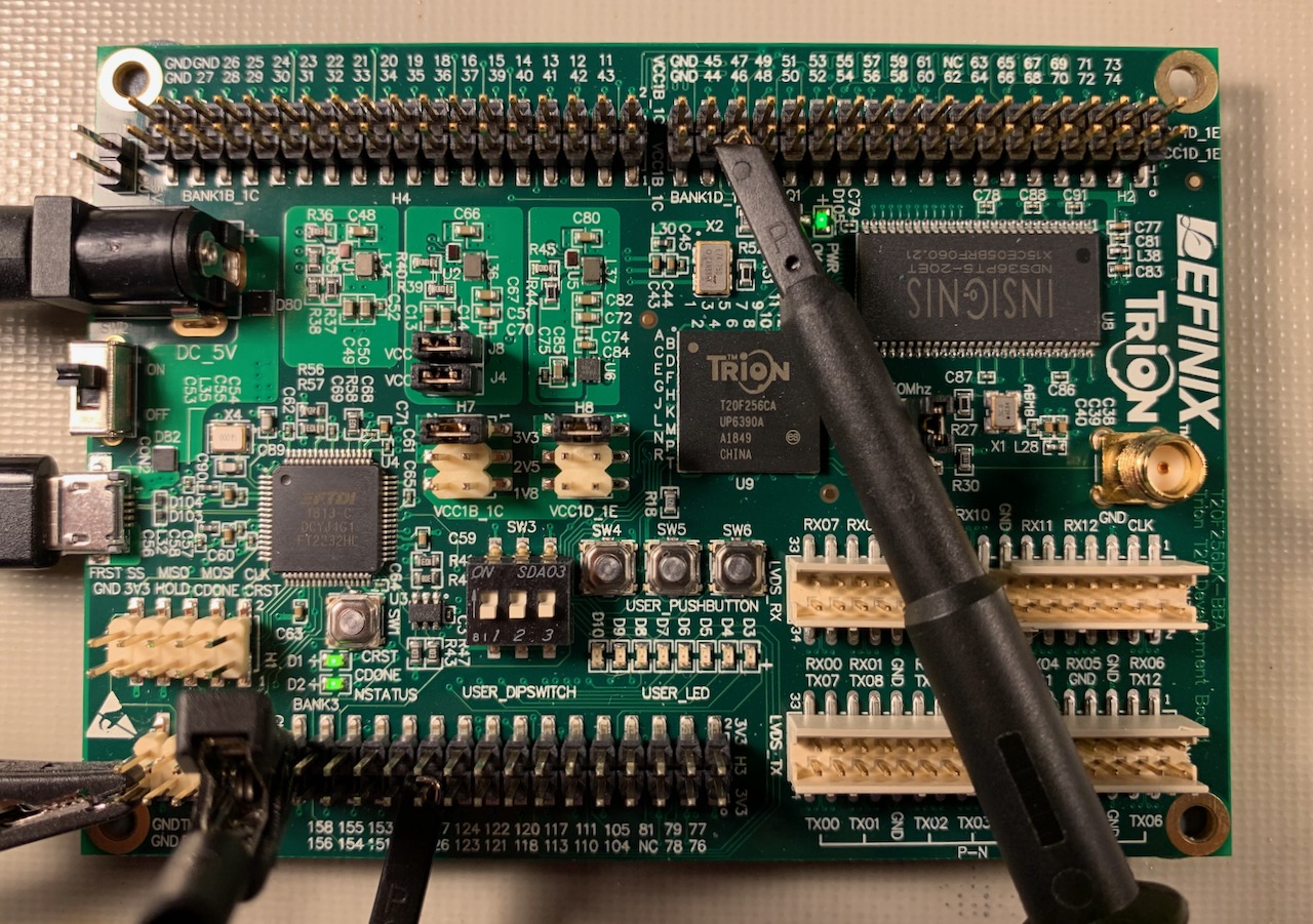
Efinix’s development kit is optimized to explore T20/T13 devices.
The Trion T20 BGA256 development kit from Efinix® is optimized to explore the many features of the easy-to-use, I/O-rich T20/T13 devices. The kit provides many ways to connect to other hardware, enabling the testing of design solutions in Trion FPGAs either by connecting it to another board for full system debug or as a stand-alone debug approach.
With the purchase of the Trion development kit, customers receive a single-seat license for the Efinity® software with one year of software maintenance, including updates and upgrades. The Efinity software provides a complete tool flow from RTL design to bitstream generation, including synthesis, place-and-route, and timing analysis. It has a graphical user interface (GUI) that provides a visual way to set up projects, run the tool flow, and view results. The software also has a command-line flow and Tcl command console. The software-generated bitstream file is used to configure the Trion FPGA on the development board with a custom design.
Features
T20 FPGA in 256-ball FBGA package
Eight user LEDs
Three user pushbutton switches, three user DIP switches
One of the things I love about JavaScritpt is the fact it keeps finding applications in different domains. One such use is in Arduino, with Espruino (open-source JavaScript interpreter for microcontrollers), and an interesting new one is the AVR8js. AVR8js is an open-source Arduino simulator based on JavaScript that can run in the cloud or virtually anywhere javascript runs.
Arduino has become a household name in the makers and hardware industry mostly thanks to it’s low-cost, easy to use the platform and the amazing community it has created over the years. Nevertheless, not everyone can always get access to an Arduino or a sensor, shield, or something to test run an idea, giving rise to the possibility of using simulators.
Arduino simulators haven’t necessarily been a household name, mostly becomes it is super easy to get an Arduino, one is probably lying next to you, and most simulators don’t work as expected as you wish. In the last 10 years, I think I have roughly tried 2 0r 3 simulators in the past: Proteus VSM and Autodesk TinkerCad. One thing familiar with most of those simulator platforms is that they are closed projects, and you are the mercy of the creators, which is something AVR8js is attempting to solve.
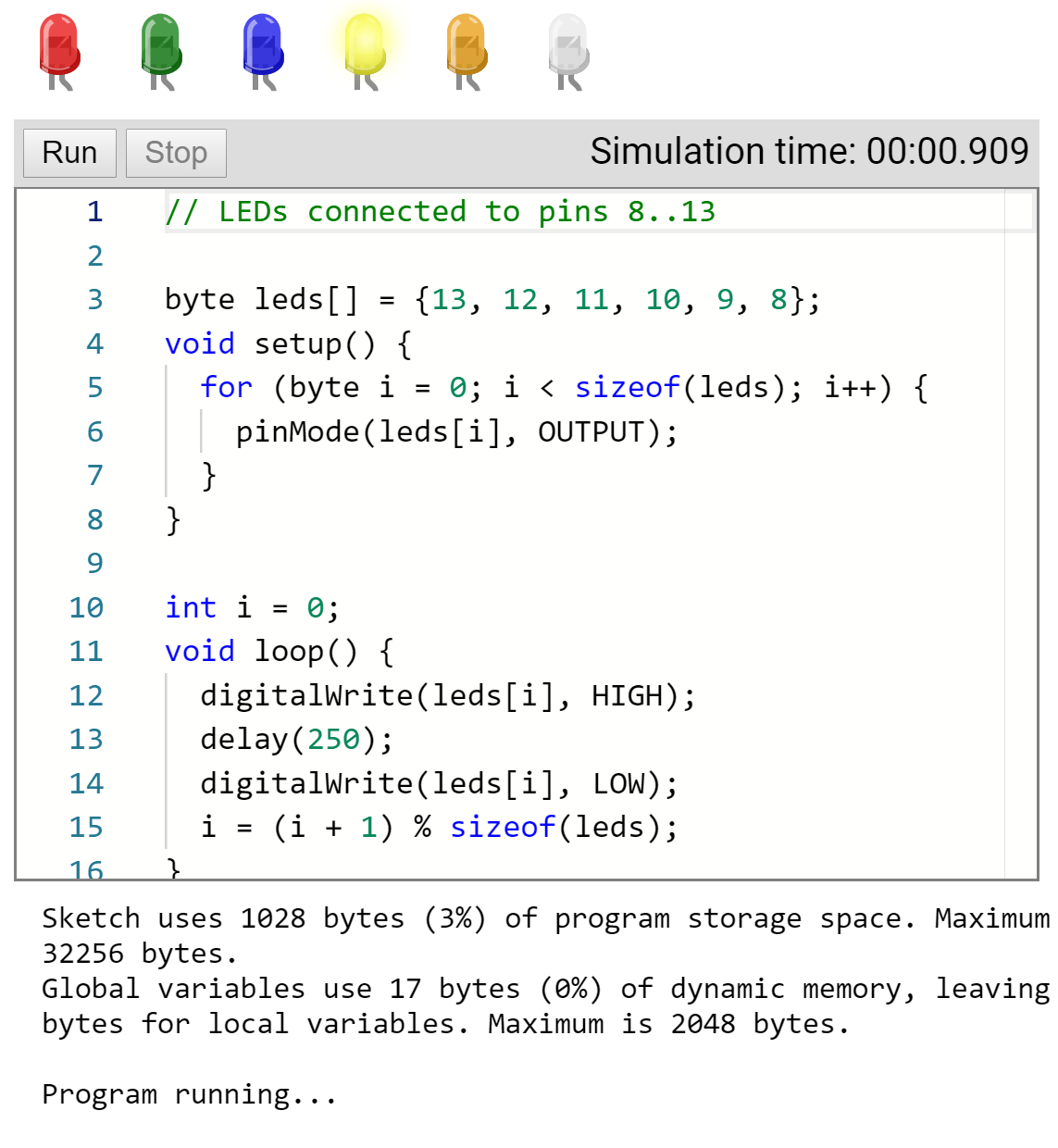
AVR8js is an AVR simulator that allows you to compile and run Arduino code directly in your browser!. AVR8js is open source in nature, and you clone the project and make modifications as you wish. Currently, there are examples of simulating multiple LEDs and even serial output.
When I write about JavaScript or other Web-related topics, I often include code samples that you can run and interact with. This allows the readers to tinker with the code and experiment further, as well as test their understanding of the subject.
I wanted to bring the same experience to my Arduino and electronics blog post. That’s how AVR8js, an open-source AVR simulator that runs inside the browser, was born.
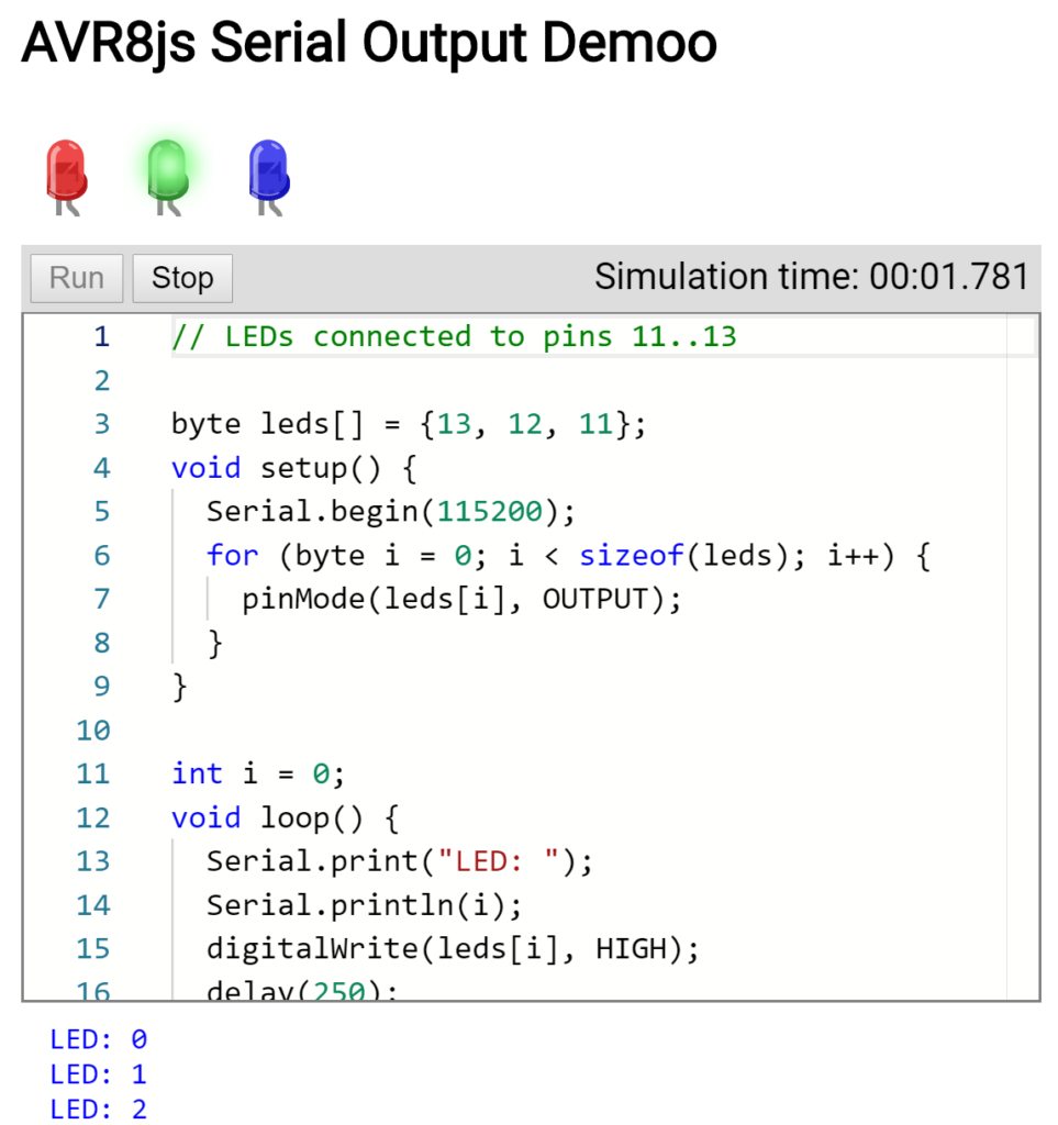
AVR8js Serial Output Demo
The code editor used for AVR8js is based on the modern Monaco Editor, the editor used with Visual Studio and provides support for syntax highlighting, automatic indentation, auto-complete, and many more. The AVR code is compiled to machine code using the Arduino CLI. More information about the AVR8js core is provided in the original post from Uri here.
Although AVR8js is still at its early stages, it has the potential of growing big mostly because of it’s open-source and the fact that it can run anywhere. More information about the project is available on the Github repo.
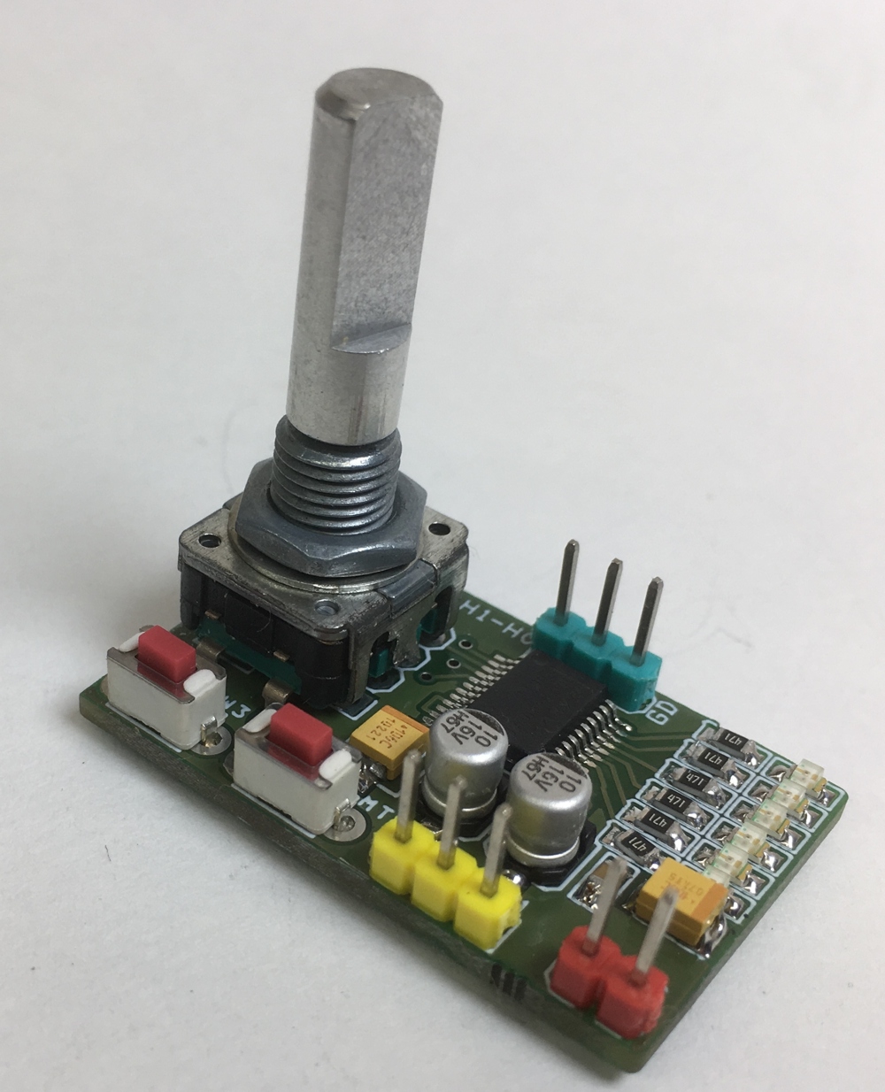
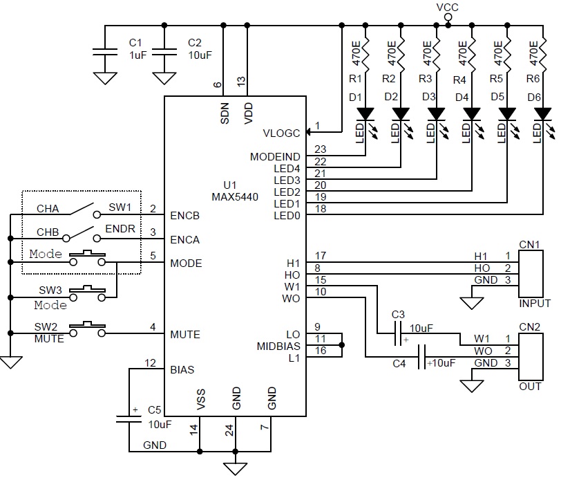
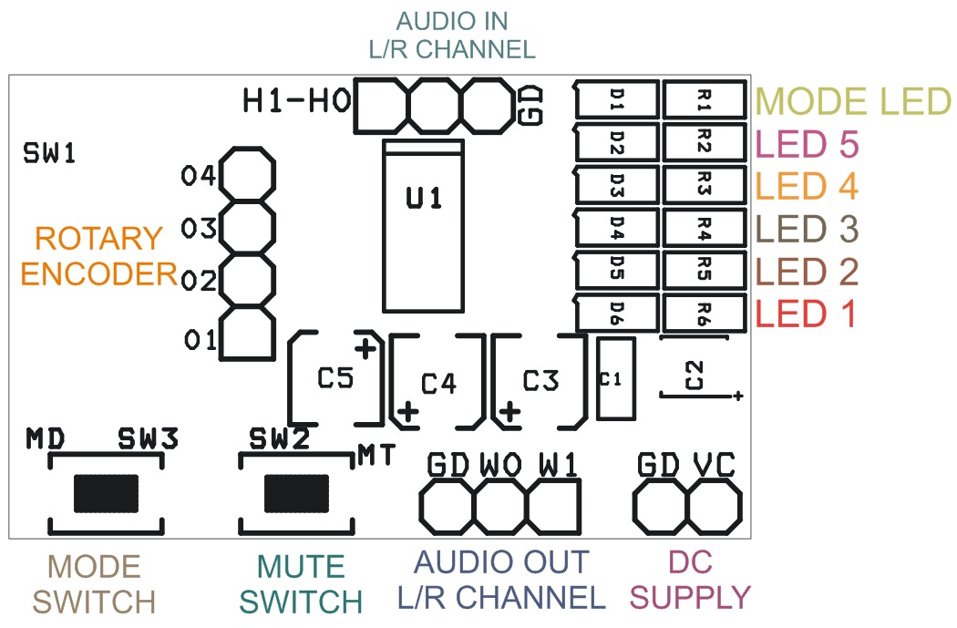
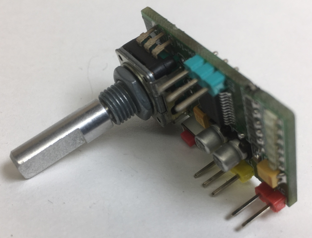
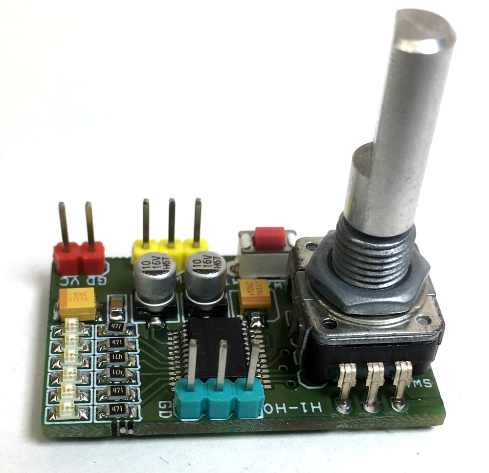
The project described here is a compact stereo volume and balance control with rotary encoder. It provides 32 log potentiometer steps with buffered wiper output. The project can easily replace mechanical potentiometer. 5 LEDs indicate the volume level or balance settings , depending on the status of the mode indicator D1 LED. The MAX5440 includes debounced pushbutton inputs for mute and mode. The mute input allows a single pushbutton to change between volume control and the -90dB (typ) mute setting. The mode input toggles between volume and balance control. A click-and-pop suppression feature minimizes the audible noise generated by wiper transitions.
MAX5440 Description
The MAX5440 dual, 40kΩ logarithmic taper volume control features a debounced up/down interface for use with a simple rotary encoder without using a microcontroller (µC). Each potentiometer has 32 log-spaced tap points with a buffered wiper output and replaces mechanical potentiometers. An integrated bias generator provides the required ((VDD + VSS) / 2) bias voltage, eliminating the need for costly external op-amp circuits in unipolar audio applications. A mode-indicator LED output specifies volume or balance control. Five integrated LED drivers indicate volume level or balance settings, depending on the status of the mode indicator.
Features
Logarithmic Taper Volume Control with (31) 2dB Steps
In the previous tutorial concerning AC resistance, we have seen that the behavior of a resistor is the same in DC or AC regime under normal frequencies. However, other basic electrical components such the inductor, strongly depends on the frequency of the AC signal.
A presentation of the concept of inductance is given in a first section in order to understand the phenomena that dictates how inductor works. A description of inductors is also given later in this same section. We explain as well why certain type of inductors are better suited for high frequency applications.
A second section highlights the dependence with the frequency of the inductance and phase shift observed in them.
Finally, a last section deals with the association of resistor and inductor in order to create filtering circuits.
Presentation
The Inductance
The inductance, is a property of an electrical component that consists of creating an opposition to the variation of the current when an alternating voltage is applied to its terminals. This moderation of the current can be explained by the electromagnetic law of induction that has been detailed in the tutorial about AC resistance.
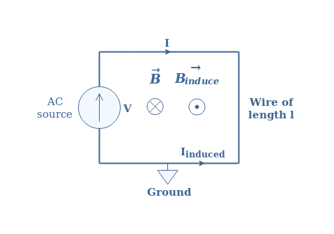
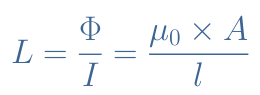
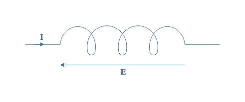
In order to understand this definition better, let’s consider a circuit that consists of an AC source and no other components other than a conductive wire of length l shorting the source as shown in Figure 1 below :
fig 1 : AC source applied to a single-wind wired
The current loop formed by the circuit creates a magnetic field B when a current I, generated by an AC source, flows into it. The circle with a cross denotes that when the current I flows as drawn in Figure 1, the magnetic field is directed downwards.
According to Lenz’s law, if the current is of AC form, B is as well alternating, which creates an induced current Ii, generated by an electromotive force E, in order to moderate the variation of the magnetic field with an induced field Bi. When the current Ii flows as shown in Figure 1, the induced magnetic field is directed upwards, which is specified by the circle with a dot.
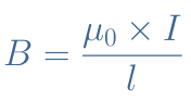
The expression of the magnetic field B is given by the following Equation 1 :
eq 1 : Expression of the magnetic field within a single-wire
Where μ0=4π×10-7 H/m is the magnetic permeability of vacuum. The magnetic flux is therefore given by Φ=B×A with A being the cross-section of the wire loop. Finally, the inductance L is given by the Equation 2 below :
eq 2 : Definition of the inductance of a single-wire
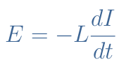
The inductance does therefore only depend on the geometry and not the source (voltage or current) and it is expressed in Henry (H). In order to understand better what this quantity represents, it is worth giving the expression of the electromotive force E in Equation 3 :
eq 3 : Expression of the electromotive force
If we isolate L in this equation, we understand that 1 Henry represents the inductance of a circuit in which an electromotive force of 1 Volt is induced when a current alternating at a rate of 1 Amp per second is flowing into it.
Inductors
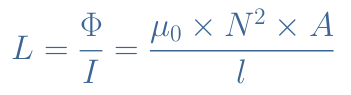
In order to considerably increase the inductance of a wire, it would be very constraining to only work on the geometrical parameters A and l. In practice, inductance components are called inductors which are wires with a certain number of turns around an axis and represented as an electrical component such as shown in Figure 2 :
fig 2 : Representation of an air-core inductor
If we consider a number N of windings, Equation 2 becomes modified to Equation 4 :
eq 4 : Expression of the inductance of an inductor
A winded wire with N turns can therefore see its inductance increased by a factor N2 in comparison with the same wire presented in Figure 1.
There is another modification that can be done with inductors to increase their inductance : add a core. The core represents the central region of the inductor, surrounded by the wire.
It can be made of a non-magnetic material such as plastic, ceramic or even air which is similar to vacuum in terms of magnetic properties. These type of inductors are known as air-core inductors and represented symbolically such as in Figure 2, they have a lower inductance but a better frequency behavior.
The other type are ferromagnetic-core inductors, their core is made from a magnetic material that increases the total magnetic permeability. Ferromagnetic-core inductors have a much higher inductance than air-core inductors because they can concentrate better the magnetic field. However, they are less suited for high frequency applications because of the important presence of Eddy currents in the core when the frequency increases, leading to losses by heat.
Ferromagnetic-core inductors can be represented such as shown below :
fig 3 : Representation of a ferromagnetic-core inductor
Frequency behavior
Reactance
It is quite ambiguous to speak about an “AC inductance” since the concept of inductance is only valid in AC regime. Indeed, considering the Equation 3 and what has been said in the previous section, one can understand that the electromotive force, the induced current and magnetic field are only existing in the presence of an AC source. As a matter of fact, in DC regime, an inductor is simply considered as a simple wire shortening a part of the circuit.
The impedance of an inductor can be defined as the opposition to the current that an inductive component generates. Impedances, such as explained during another tutorial, are complex numbers which have a real part representing a resistance and an imaginary part representing a reactance.
For an inductor, the reactance XL represents the opposition of the component to a change of current. The impedance of an inductor is a pure imaginary number, meaning that no resistance is considered and its reactance is given in the following formula :
eq 5 : Reactance of an inductor
The opposition to an AC current increases therefore linearly with the frequency. At f=0 Hz (DC regime), the inductor as previously said act as a short circuit and when f→+∞, it acts as an open circuit.
Phase shift
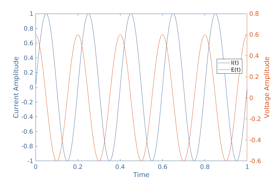
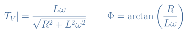
The impedance of the inductor is simply given by ZL=jXL. The phase shift φ between the current across the inductor and the voltage generated at its terminals (electromotive force) is constant and given by Arg(ZL)=arctan(y) with y→+∞, which gives φ=+π/2 rad or 90°.
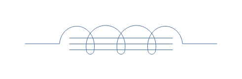
This particular value of phase shift, as emphasized in the tutorial about phase splitters, is called a quadrature phase advance and illustrated in Figure 3 :
fig 3 : Illustration of the quadrature phase shift in an inductor. Plotted with MatLab®
If the amplitude (reference to peak) of the current is given by Imax, the amplitude of the electromotive force is Vmax=Imax×XL.
Induction phenomena
When the AC source frequency increases, similar phenomena that have already been described in detail in the AC resistance tutorial take place inside inductors.
The first one is the skin effect, it is caused by a redistribution of the current near the border of the wire constituting the inductor. This high concentration of the current in a small region increases the resistance of the inductor, which as a consequence, lead to heat losses.
The proximity effect is also very present in inductors. Indeed, each turn of wire induces Eddy currents in the border region of their neighbors wires. Such as for the skin effect, this tends to reduce the effective cross-section for the current which increases the resistance.
RL filters
We have seen with this tutorial that inductors are very sensitive to the frequency but on the other hand, resistors are not. So the natural question that comes is what happens if we combine these components in a same circuit ?
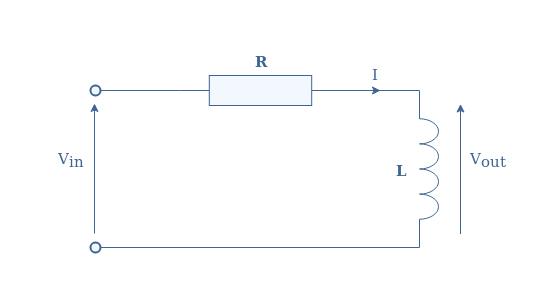
Let’s therefore consider a RL circuit which input voltage is noted Vin and output voltage Vout :
fig 4 : Series RL circuit
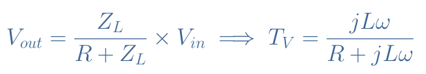
We call TV the transfer function of the circuit which is defined by the ratio Vout/Vin. In order to find the expression of TV, we can simply look at the circuit as a voltage divider. As a consequence, we have :
eq 6 : Expression of the RL circuit transfer function
This function is interesting because it gives us simultaneously the voltage gain and phase shift of the circuit for any frequency.
The gain is given by the module of TV and the phase shift Φ by its argument, both are given in Equation 7 below. We recommend to the reader to refer to the tutorial about complex numbers in order to know how to determine the module and argument of a complex fraction.
eq 7 : Gain and phase shift of a RL circuit
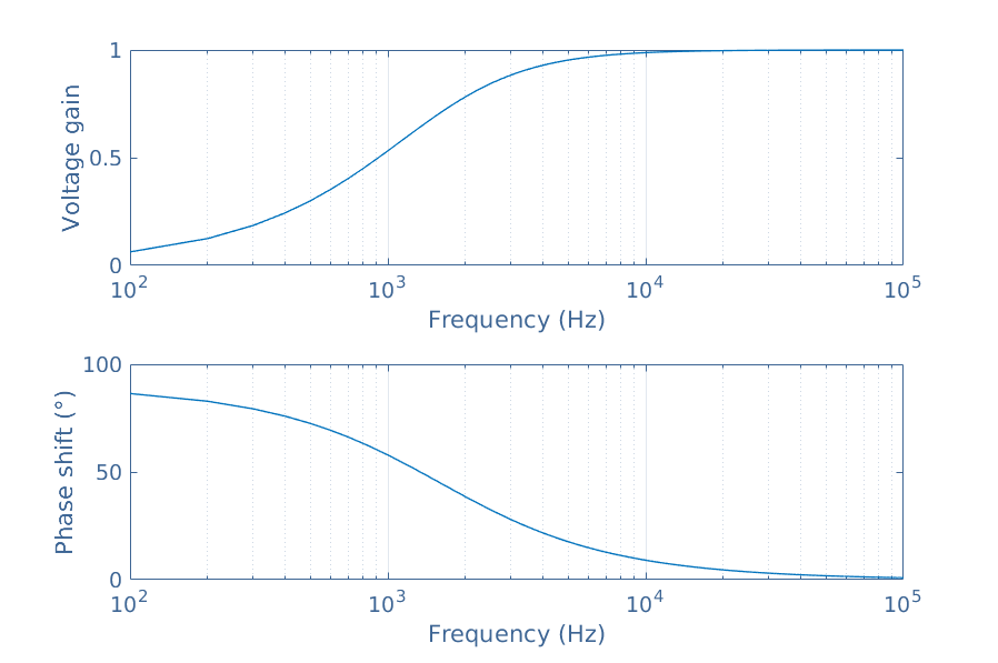
Let’s take R=1 kΩ and L=100 mH and plot the two quantities presented in Equation 7 in logarithmic scale for the frequency. The resulting plot is commonly known as a Bode diagram and shown in Figure 5 :
fig 5 : Bode diagram of the RL circuit
At low frequency (DC regime) the inductance impedance is negligible, therefore the voltage drop is completely absorbed by the resistance and none in the inductance. A quadrature phase shift is observed in DC regime.
At high frequency, the inductance impedance prevails and the voltage drop is therefore absorbed by the inductance which gives a gain that tends to 1. The phase shift tends to zero as the frequency increases.
As a conclusion, we can say that an RL circuit acts as a high pass filter since the low frequencies are not transmitted.
Conclusion
It as been shown during this tutorial that inductors behave differently than resistor with change of frequency.
First of all, a presentation of the concept of inductance has been given. The inductance is an important factor to understand the induction law, it describes how strong a component will react with a change of the current within a circuit. Later, through the presentation of inductors, we have seen that the inductance can be increased with windings and with the presence of a magnetic core.
In a second section, we looked more closely to the frequency behavior of inductors. Their impedance increases linearly with the frequency, in DC regime they behave as short circuits and become open circuits when the frequency is very high.
Combining inductors with resistors has been investigated in a last section. We have shown how to describe the behavior of a RL filter with the concept of transfer function and Bode diagram.
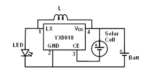
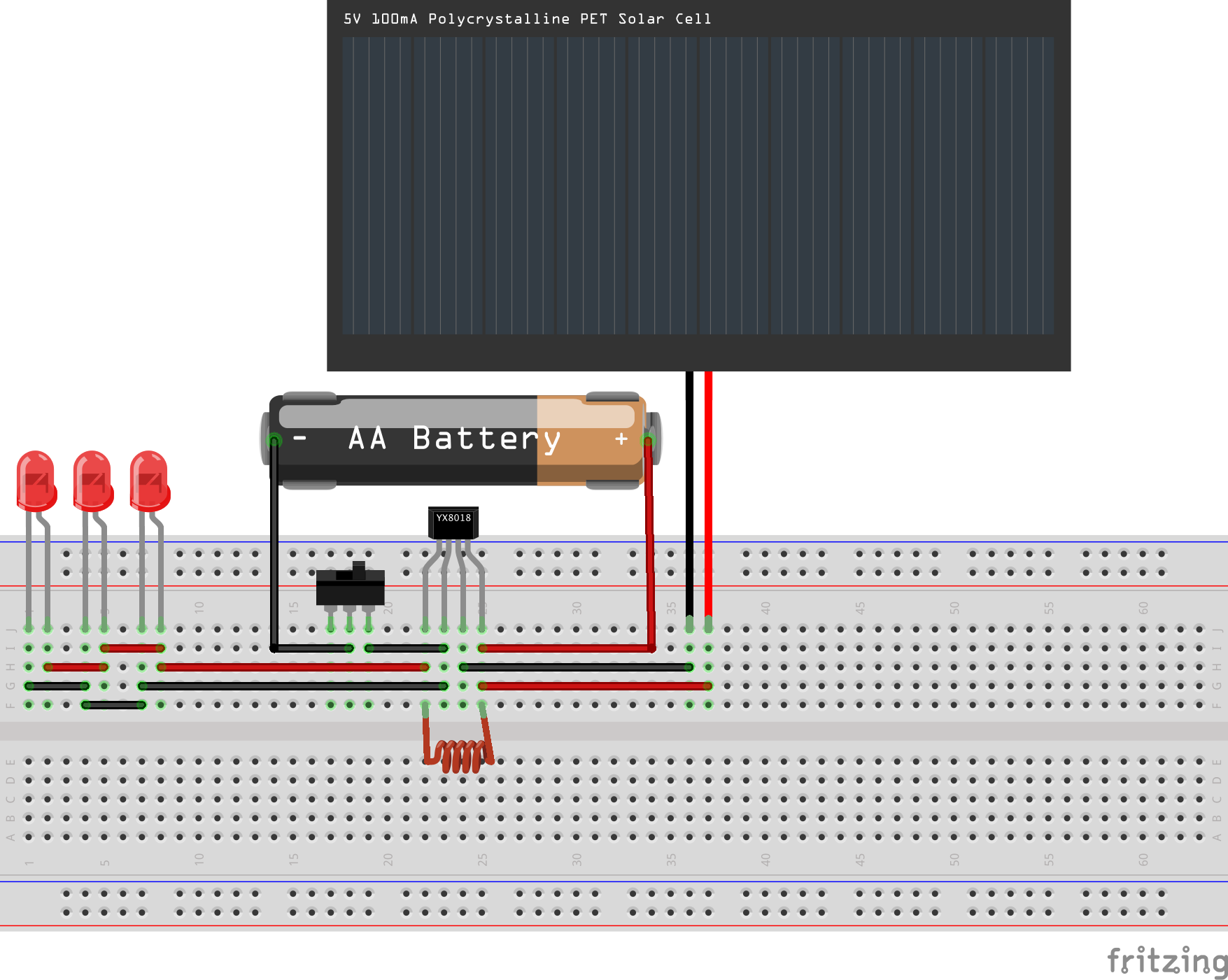
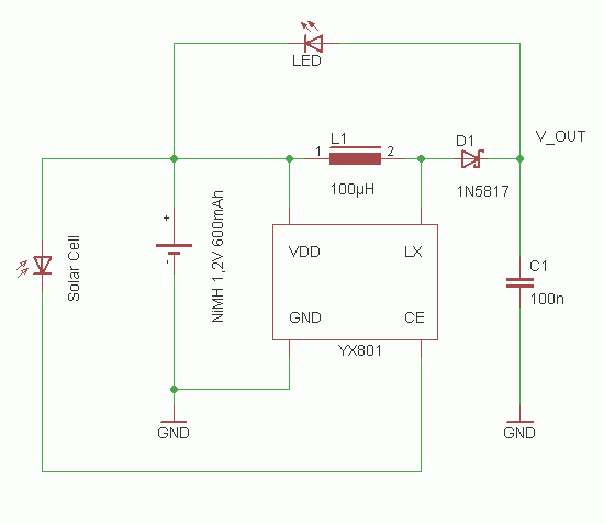
YX8018 is a 4-pin integrated circuit for driving solar powered garden LED lights and is found on many cheap garden lights. You can buy 10x YX8018 ICs on AliExpress for around $1. You will need the following parts to build one on your own:
Parts
i-Cd AA 300mAh 1.2v rechargable battery
YX8018 solar LED driver IC, TO-94 package
Solar panel, 5cm x 5.5cm
3x white LED
100 Microhenrys +/-10% inductor (brown black brown silver)
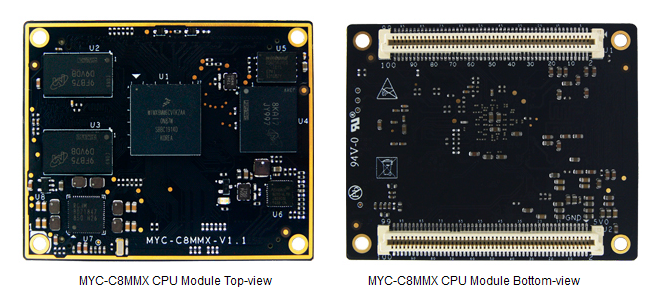
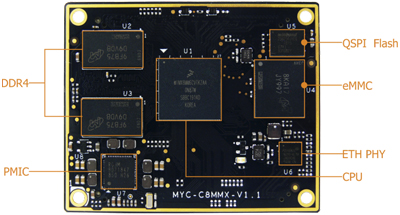
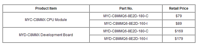
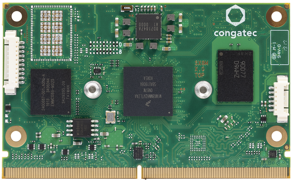
MYIR introduces a high-performance and cost-effective ARM SoM MYC-C8MMX CPU Module powered by i.MX 8M Mini which is NXP’s first embedded multi-core heterogeneous applications processors built using advanced 14LPC FinFET process technology. The processor on this module features up to 1.8GHz quad-core ARM Cortex-A53 plus 400MHz Cortex-M4 processor. The module runs Linux, Android OS and is capable of working in industrial temperature ranging from -40°C to 85°C.
Measuring 60mm by 49mm, the MYC-C8MMX CPU Module provides an outstanding embedded solution for Home and Building Control, IOV, Industrial and Medical Instruments, Human Machine Interface (HMI) and more other general purpose industrial and IoT applications which require optimized power consumption while maintaining high-performance.
The MYC-C8MMX CPU Module is a minimum system integrated with CPU, 2GB DDR4, 8GB eMMC, 32MB QSPI Flash, GigE PHY and PMIC. All controller signals are brought out through two 0.8mm pitch 100-pin Expansion Connectors.
MYC-C8MMX CPU Module
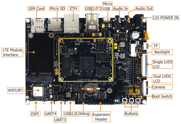
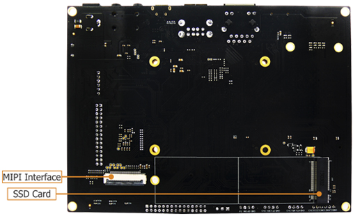
MYIR offers MYD-C8MMX development board for evaluating the MYC-C8MMX CPU Module, the base board has taken great media capabilities of the i.MX 8M Mini processor to provide MIPI-DSI, MIPI-CSI, LVDS interfaces and Audio In/Out ports. It also has strong communication connectivity with 2 x USB 2.0 Host ports and 1 x Micro USB 2.0 Host/Device port, Gigabit Ethernet, MicroSD card slot, USB based Mini PCIe interface for 4G LTE Module, WiFi/Bluetooth and NVMe PCIe M.2 2280 SSD Interface. MYIR can offer design services to help customize the base board according to customers’ requirements.
MYD-C8MMX Development Board Top-view
MYD-C8MMX Development Board Bottom-view
MYIR offers commercial and industrial options for CPU Modules and Development boards. The prices are economic. Discount is said to be offered for volume quantities which can be as low as $49.80.
More information about above new products can be found at:
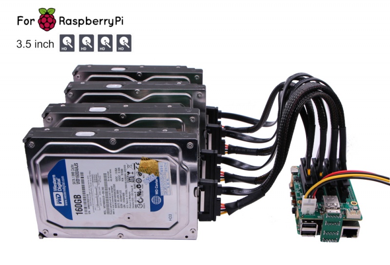
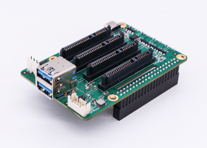
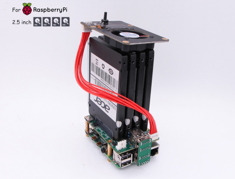
Radxa is very happy to announce the ROCK Pi SATA HAT, a series of SATA expansion targeting at the NAS solution for Raspberry Pi 4 and ROCK Pi 4. The ROCK Pi SATA HATs come in 3 models:
Dual/Quad SATA HAT
Penta SATA HAT
The Dual/Quad SATA HAT is designed for Raspberry Pi 4 as well as ROCK Pi 4, and the Penta SATA HAT is designed for ROCK Pi 4 only.
Dual/Quad SATA HAT
The Dual/Quad SATA HAT utilize the USB3 buses on Raspberry Pi 4 or ROCK Pi 4, it has the following features:
Up to 4x HDD/SSD, support 2.5inch or 3.5inch SSD
Utilize two independent USB3 buses on Raspberry Pi 4
Type C power input with USB PD/QC support for both 2.5inch SSD and Raspberry Pi 4
External standard ATX power supply support for 3.5inch HDD
Fan and heatsink for Raspberry Pi 4 CPU cooling
Support HDD suspend mode
Support UASP
Support software RAID 0/1/5
Optional PWM control fan for HDD heat dispatching
Optional OLED display for IP Address/Storage info
For 3.5 inch HDD, a standard ATX PSU is required to power the HDD and the Raspberry PI itself. With 4 3.5inch HDDs, the PSU should be 60W or more.
For 2.5 inch HDDs, you can just use the USB PD/QC power adapter(30W power adapter is enough) to power the HDD/SSD and the Raspberry Pi 4 itself.
Performance
Quad SATA HAT utilizes two high performance JMS561(one JMS561 for Dual SATA HAT) providing up to 400MB/s reading/writing performance with four disks in RAID0 mode.
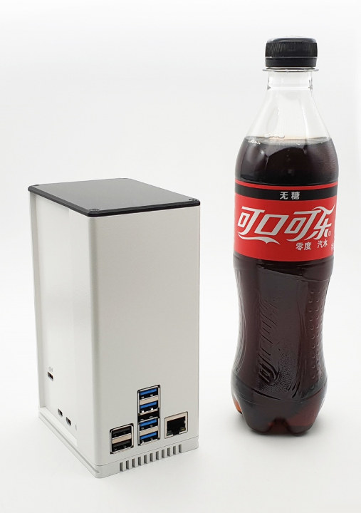
RPi 4 NAS Enclosure
The boards can now be pre-ordered as follows:
$25 Quad SATA HAT for Raspberry Pi 4 / Rock Pi 4
$49 Penta SATA HAT for Rock Pi 4
$8 SATA HAT Top Board
$99 for Quad SATA kit for Raspberry Pi 4 with enclosure. Raspberry Pi 4 not included.
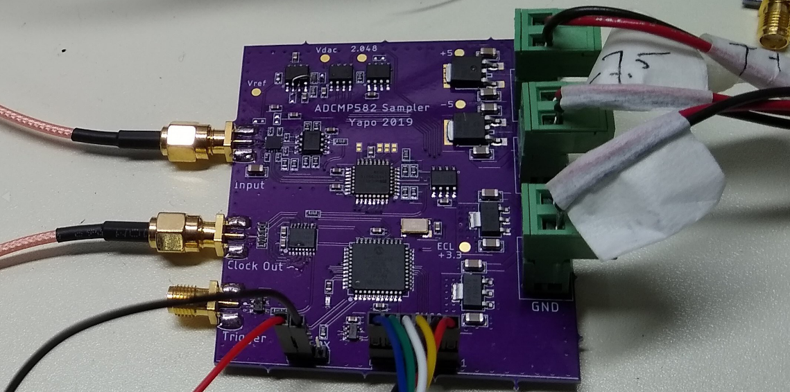
A basic open-source multi-GHz sampling oscilloscope for experimenters on a budget. Still a work-in-progress, with key pieces on separate PCBs, but showing bandwidths in the 7-8 GHz range with >= 100 GSa/s equivalent-time sampling, and around 500 k comparisons/second real time. by Ted Yapo @ hackaday.io
This particular project uses a latched comparator as a voltage sampler, specifically the ADCMP582 from Analog Devices. Built on SiGe, this $20 (single-quantity) comparator has a sampling aperture of 5 ps, and a typical front-end bandwidth of 8 GHz. This ultimately limits the bandwidth of the resulting instrument, but other factors in the current design reduce the system bandwidth into the 6 GHz range. Very preliminary tests estimate the rise time of the scope to between 50 and 70 ps, corresponding to between 7 and 5 GHz bandwidth, respectively. I’m calling it 6 GHz for now, and I expect it can be improved somewhat,
8 GHz Sampling Oscilloscope for experiments – [Link]
Congatec is introducing a new CoM, the Conga-SMX8-Nano that offers up to 4x ARM Cortex-A53 and 1x Cortex-M7 core along with 1,000’s of different possible configurations. This SMARC 2.0 module based on NXP i.MX 8M Nano processor series can meet ultra-low-power requirements with high-level performance while being very cost-effective.
Conga-SMX8-Nano module featuring the i.MX8M Nano offers up to 4x 14nm-fabricated Cortex-A53 cores with a boost clock frequency of 1.5GHz. It also has a Vivante GC7000UL 3D/2D GPU with support for OpenGL, OpenCL, and Vulkan. There’s also a powerful 600MHz Cortex-M7. This new module is also rated for 2W TDP.
The default SKU houses 16GB eMMC 5.1 with support to expand to up to 128GB and 2GB LPDDR4 (3200 MT/s) DRAM. The module has a GbE controller with IEEE 1588 support and an optional WiFi/Bluetooth M.2 card. The Conga-SMX8-Nano supports a dual-channel 24-bit LVDS, or alternatively, an optional eDP 1.4 or 4-lane MIPI-DSI interface. There is a single USB 2.0 host or OTG interface and it also supports up to 4x USB 2.0 ports via a hub. The dimension of the module is 82 x 50mm. The standard module has an operating temperature range of 0 to 60°C while being clocked at 1.5GHz, but industrial models back the clock down to 1.4GHz to support -40 to 85°C range.
Other highlighted specifications are MIPI-CSI x2 and x4, up to 3x UART, multiple GPIOs, 2x I2S, and single SDIO 3.0, I2C, and SPI connections. There are many security features like cryptography, RNG, 32KB secure RAM, and High Assurance Boot. The module has a watchdog, JTAG debug, and optional RTC. The company has assured up to 15 years of lifecycle support for this module.
conga-SMX8-Nano Rear View
Spec List for Conga-SMX8-Nano:
Form factor – SMARC 2.0
CPU – NXP i.MX 8M Nano Quad (4x 1.5GHz ARM Cortex-A53, 1x 750MHz ARM Cortex-M7)
DRAM – Up to 2 GByte onboard LPDDR4 memory (3200 MT/s)
Ethernet – 1x Gigabit Ethernet with IEEE 1588 support
I/O Interfaces –
1x USB 2.0 or 1x USB OTG client
1x SDIO 3.0
I²C bus
SPI up to 3x UART
GPIOs optional M.2 1216 WiFi/BT module
Graphics – Integrated into NXP i.MX 8M Nano Series GC 7000UL 3D GPU
Operating Systems – Linux, Android, Yocto
Operating Temperature Range –
Extended Commercial : Operating: 0 to +60°C Storage: -20 to +70°C
Industrial: Operating: -40 to +85°C Storage: -40 to +85°C
Humidity – Operating: 10 to 90% r. H. non-cond. / Storage 5 to 95% r. H. non-cond.
Video Interfaces – 1x dual-channel 24bit LVDS (default), optional eDP 1.4 or MIPI-DSI 4-lanes (shared with LVDS)
Size – 82 x 50 mm (3,23” x 1,97”)
No pricing or availability information is available yet for the Conga-SMX8-Nano. More information may be found in Congatec’s announcement and product page.
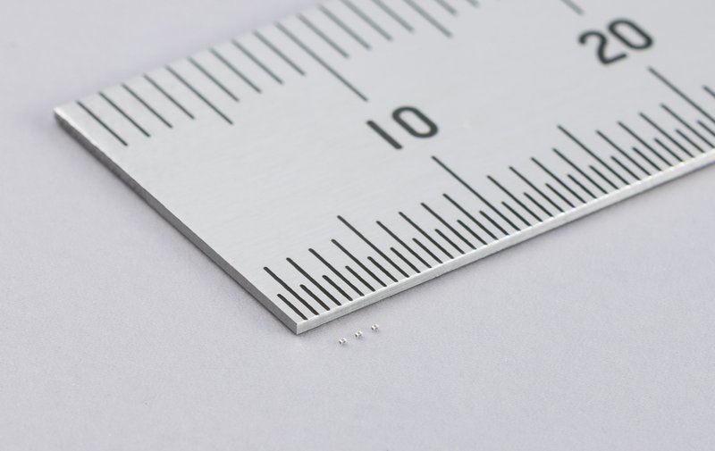
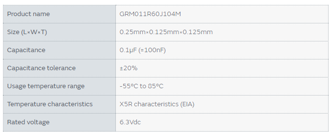
Murata Manufacturing Co., Ltd. has developed the GRM011R60J104M, the world’s first multi-layer ceramic capacitor to feature a maximum capacitance of 0.1µF in 008004 inch size (0.25×0.125mm). Mass production of this new product is scheduled to begin in 2020.
As smartphones supporting 5G become more widespread and devices such as wearable devices become increasingly multifunctional and more compact, the demand for smaller and higher density electronic circuitry is growing. Among the components employed in this circuitry, multi-layer ceramic capacitors are essential for electronic devices and are used for a wide range of applications such as in smartphones and wearable devices. As the high end smartphones are equipped with around 800 to 1,000 capacitors, there is a considerable need for such components to be made even more compact.
By using our original ceramic and electrode material atomization and homogenization technology, Murata has achieved a mounting surface area approximately 50% smaller and a volume approximately 80% smaller than that of our conventional product (01005 inch size) with a capacitance of 0.1µF. Moreover, the new product has a capacity of around 10 times that of the same-sized product (008004 inch size) initially mass-produced by the Company.
Specifications
In future, Murata will continue to conduct research and development into ceramics and high-precision, microscopic layering technology for electrode materials, expand our lineup to meet the needs of the market, and contribute to the further miniaturization and greater functionality of electronic devices.