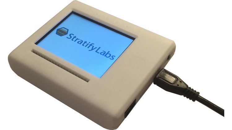
As a hardware developer, I keep a number of tools and gadgets handy such as a USB to UART converter, O-scope, multi-meter, SWD/JTAG programmer, jumper wires as well as a few others depending on the situation. The Stratify Toolbox will replace all of these and more.
Features
The Stratify Toolbox is a Wi-Fi-enabled, all-in-one hardware/firmware development tool. It can
Analyze serial protocols
Log data on it’s SD card (JSON, YAML, TSV)
Display analog/digital waveforms on the built-in IPS display
Program and debug microcontrollers using SWD/JTAG
Generate signals
Execute applications developed by anyone using the SDK
Do all of the above from anywhere in the world using a Wi-Fi connection
Specifications
480 MHz ARM Cortex-M7 processor (STM32H750)
100 KB’s of RAM for user applications
8 MB QSPI flash (for kernel updates, fonts, user data)
MicroSD card slot (supports SDHC with FAT filesystem)
Mixed-mode regulation merges a switch-mode power conversion design with linear final regulation to give excellent noise and transient characteristics resembling linear supply performance but at greatly reduced weight.
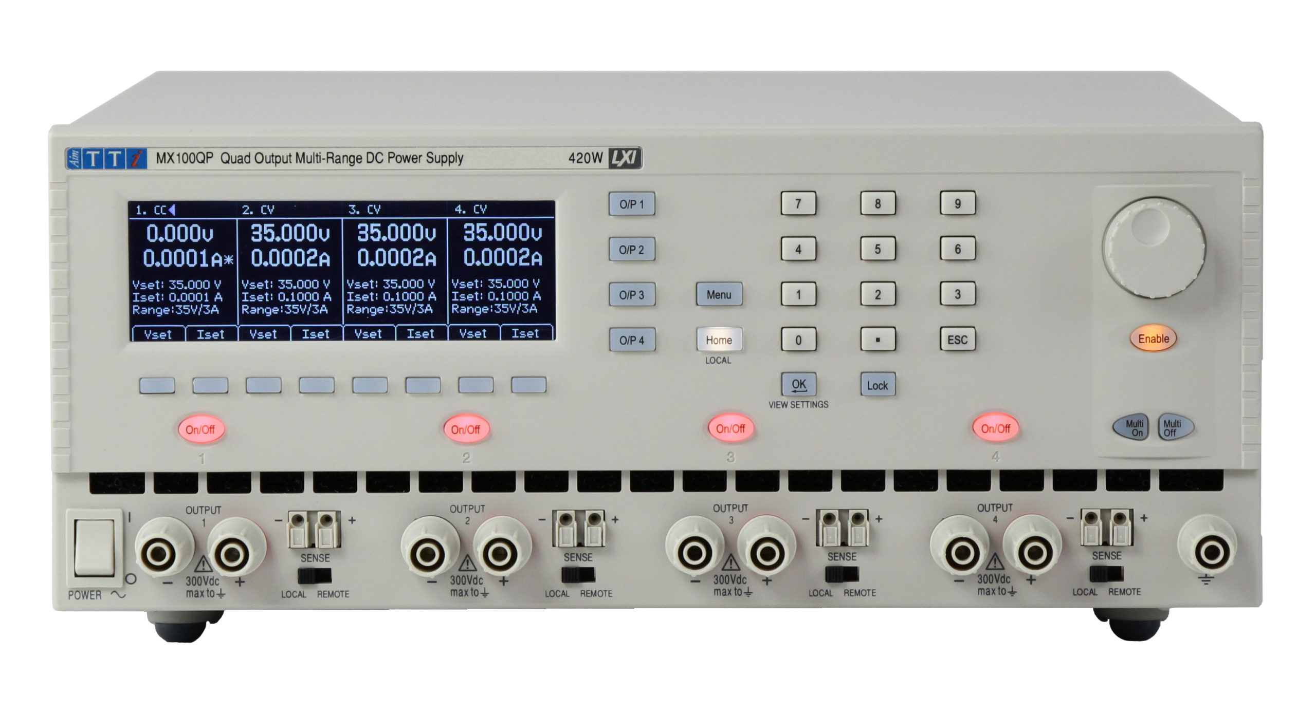
Saelig Company, Inc. has announced the introduction of the AIM-TTi MX100Q Series Power Supplies, versatile 4-output laboratory power sources which use mixed mode regulation to provide up to 210W of power, shared by up to four outputs, in one compact case. Mixed-mode regulation combines switch-mode architecture with linear final stage regulation to give performance characteristics resembling a totally linear design but at greatly reduced weight. Each output can provide 0 to 35 volts at 0 to 3 amps, with output combination abilities that extend output voltages up to 70V and currents up to 6A. The MX100Q series provides fine precision output adjustment with a resolution of 1mV and 0.1mA. All relevant information is displayed on a large backlit graphic LCD, with control is via soft keys, a numeric keypad, and a spin wheel.
More than 50 standard range output combinations are available. Advanced features include 50 memorized settings for each output plus 50 further settings for all four outputs together. Multi-On and Multi-Off keys supplement the individual output On/Off keys. Keys can be programmed to turn the outputs on or off in a timed sequence. The front panel can also be locked to prevent accidental changes to settings.
The MX100Q power supply is housed in a ¾ rack width, 3U high case with front input ventilation. An intelligent fan design minimizes cooling noise. The MX100QP version also adds USB, RS232, GPIB (optional) and LXI compliant LAN interfaces, plus duplicate rear-mounted power and sense terminals.
Key Features of the MX series include:
Four independent and full performance outputs
Simultaneous display of meters and settings for all outputs
Instant access to voltage/current setting for any output
Multiple ranges on each output for wider voltage/current choice
Instant individual on/off control plus sequenceable multi on/off
Up to 250 memory settings for individual or multiple outputs
Typical applications for the MX100Q range include: medium to high power bench-top applications requiring multiple outputs; situations where voltage and current requirements may vary widely between projects; powering rail-sensitive circuits using on/off sequencing; repetitive testing applications requiring memorized multi-output settings memories; high-density system applications requiring multiple outputs with limited rack space; remote power control applications.
Made by Aim-TTi, a leading European test equipment manufacturer, the MX100Q series is available now from Saelig Company, Inc., Fairport, NY.
Thanks to their tiny size and improved capabilities, the ATtiny-0-Series of microcontrollers have been a delight for designers and DIYers looking for a microcontroller with the ease of use associated with the Arduino boards, but with a way smaller form factor associated with ATtiny microcontrollers. Along with the ATtiny-1-series, the ATtiny-0-Series microcontrollers were meant to serve as a modern replacement for other popular ATtiny chips like the ATtiny85 and ATtiny45. While they have been able to do these with incredible features one challenge users have had over time includes; difficulties in programming the chips, as, unlike the previous ATtiny chips, they use a not so popular programming protocol called UPDI in place of the ISP protocol used by the previous series.
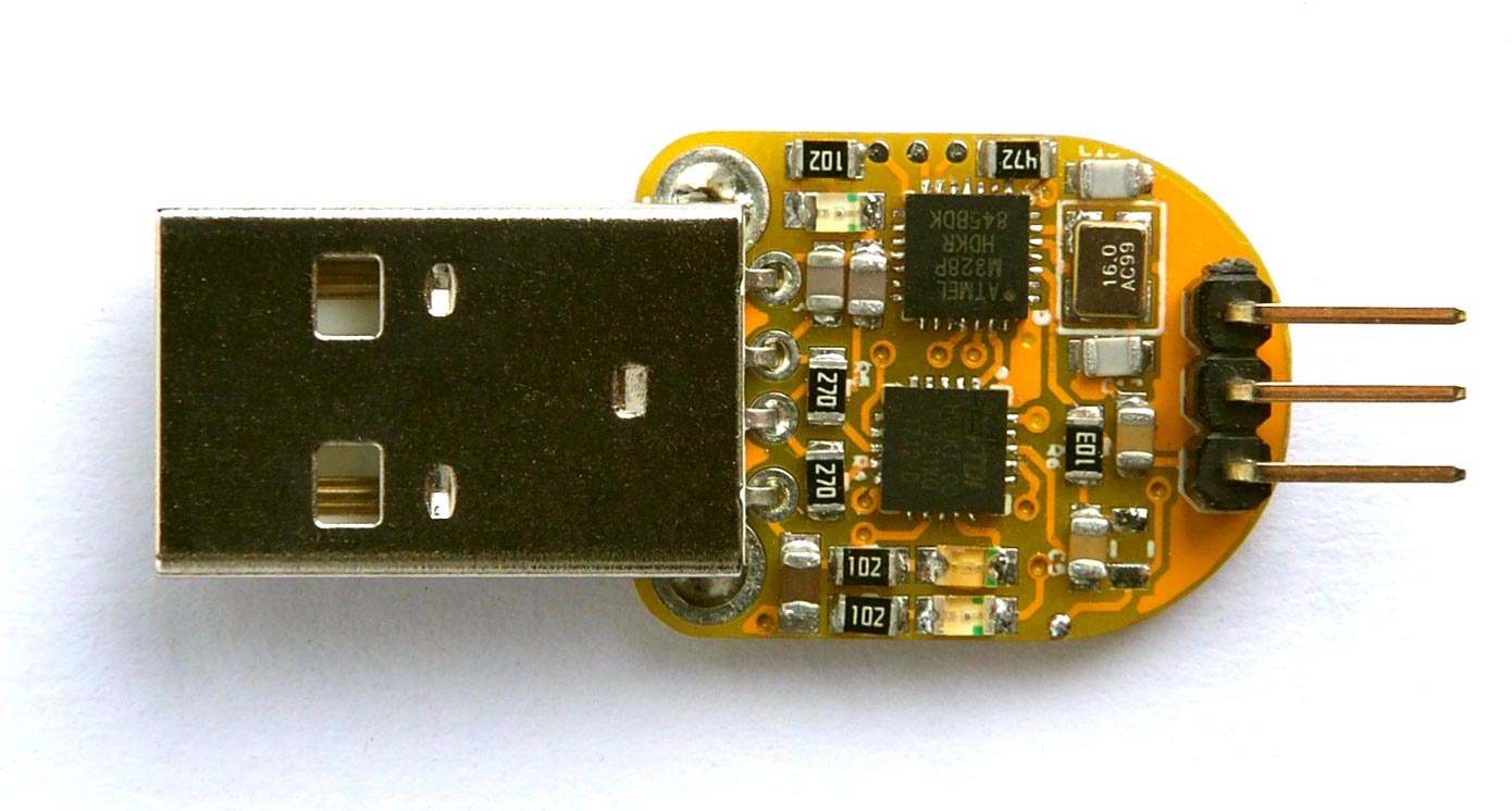
To solve this, several programmers have developed various ways through which the Attiny-0-series can be programmed. One of them was discussed in one of our previous tutorials, but for today’s tutorial, we will look at the most elegant way we have seen so far; the UPDI Programming Stick developed by David Johnson-Davies.
This programmer is based on the Atmega328P and can really be said to be an Arduino Uno on USB. It uses the Atmega328P microcontroller as the UPDI programmer while the FT231 serves as the USB to UART converter facilitating data exchanges between the programmer and the computer. As mentioned above, the device can also be used as a limited Arduino Uno, for the reason that the digital pin 6 of the Atmega328P which is compatible with the pin 6 on an Arduino Uno, is broken out so it can be used for Arduino related acts.
While the programmer can be bought from different electronics component online stores, the maker in us would love to build our own and since the design is open-source we have all we need.
Thus for today’s tutorial, we will examine how you can build your own version of the UPDI Programmer stick.
Program ATtiny 0-Series Chips with a Miniature UPDI Dongle – [Link]
Synchronous DC/DC Buck Regulators Feature Lower Quiescent Current and Proprietary Light Load Mode to Achieve up to 6% Higher Efficiency in Standby Mode
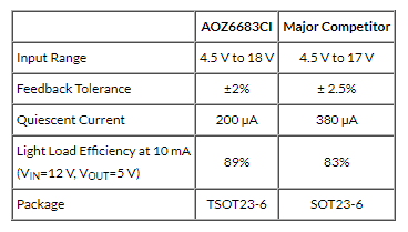
Alpha and Omega Semiconductor (AOS) introduced AOZ6682CI and AOZ6683CI. These devices are high efficiency, simple-to-use synchronous buck regulators. The AOZ6682CI and AOZ6683CI are both available in an ultra-thin, thermally enhanced TSOT23-6 package and deliver 2 A and 3 A output current, respectively. The new devices offer high efficiency over the full load range, allowing greener power conversion for a variety of consumer electronics applications such as LCD TVs, set-top boxes, high definition Blu-Ray™ Disc Players and Networking terminals.
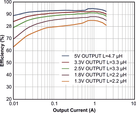
The AOZ6682CI’s Efficiency vs Output Current. VIN = 12 V.
The new devices incorporate a low resistance synchronous buck power stage that enables up to 95% efficiency. Combined with a thermally enhanced package, the AOZ6682CI and AOZ6683CI achieve 10 °C cooler operation at full load compared to similar competing devices. Under heavy load conditions, the devices operate in a fixed frequency continuous-conduction mode (CCM). At light loads or in standby mode, the devices employ a proprietary pulse energy mode (PEM) control scheme. This control scheme and low quiescent current of 200 µA, allows the buck converter design to achieve industry-leading efficiencies of 89% at light loads.
Pricing and Availability
The AOZ6682CI and the AOZ6683CI are immediately available in production quantities with a lead time of 12 weeks. The unit price is $0.42 for the AOZ6682CI and $0.52 for the AOZ6683CI in 1000 pc quantities.
Thanks to their tiny size and improved capabilities, the ATtiny-0-Series of microcontrollers have been a delight for designers and DIYers looking for a microcontroller with the ease of use associated with the Arduino boards, but with a way smaller form factor associated with ATtiny microcontrollers. Along with the ATtiny-1-series, the ATtiny-0-Series microcontrollers were meant to serve as a modern replacement for other popular ATtiny chips like the ATtiny85 and ATtiny45. While they have been able to do these with incredible features one challenge users have had over time includes; difficulties in programming the chips, as, unlike the previous ATtiny chips, they use a not so popular programming protocol called UPDI in place of the ISP protocol used by the previous series.
UPDI Programming Stick
To solve this, several programmers have developed various ways through which the Attiny-0-series can be programmed. One of them was discussed in one of our previous tutorials, but for today’s tutorial, we will look at the most elegant way we have seen so far; the UPDI Programming Stick developed by David Johnson-Davies.
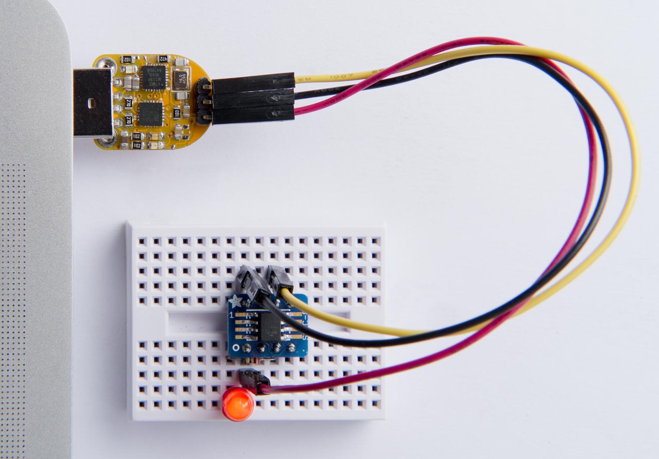
This programmer is based on the Atmega328P and can really be said to be an Arduino Uno on USB. It uses the Atmega328P microcontroller as the UPDI programmer while the FT231 serves as the USB to UART converter facilitating data exchanges between the programmer and the computer. As mentioned above, the device can also be used as a limited Arduino Uno, for the reason that the digital pin 6 of the Atmega328P which is compatible with the pin 6 on an Arduino Uno, is broken out so it can be used for Arduino related acts.
While the programmer can be bought from different electronics component online stores, the maker in us would love to build our own and since the design is open-source we have all we need.
Thus for today’s tutorial, we will examine how you can build your own version of the UPDI Programmer stick.
Required Components
Since the idea behind the project is to make a solid board, the project is implemented on a PCB and to reduce the size, most of the components used were SMD, with the USB Male-type connector being the only through-hole component. The components used are provided in the table below;
The fact that most of the components listed above are SMD, means, to be able to build the project successfully, it is important that you have all you need for SMD Soldering, including the tools (like a reflow oven/Hot air gun), skill and experience, especially when it comes to soldering the QFN package components. For those who do not have access to SMD soldering requirements, the Breadboard version of the project can also be built using a through-hole version of the components.
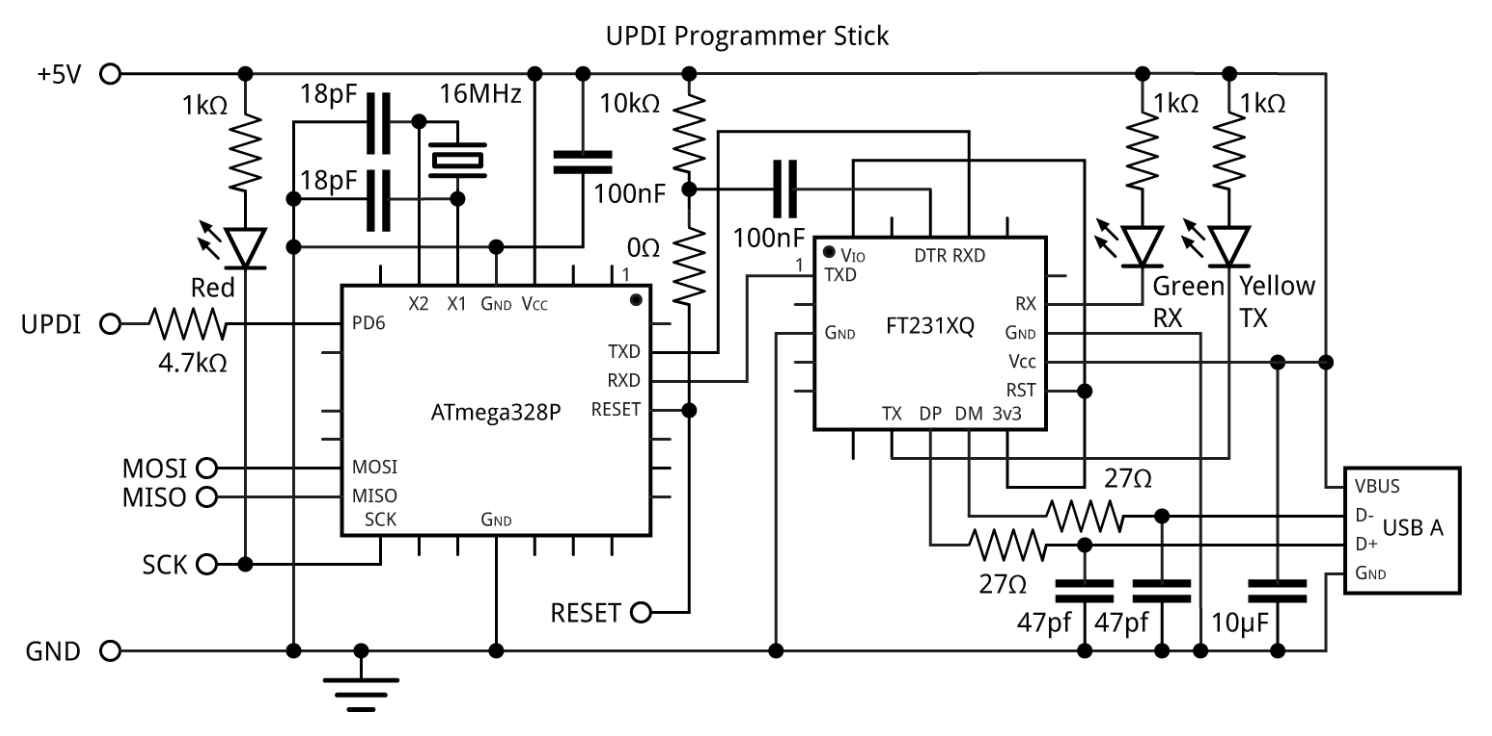
Schematics
The schematic for the project is provided in the image below:
It features two main ICs: the Atmega328p microcontroller and the FT231 USB to UART Converter. The ATmega328p acts as the UPDI programmer and the FT231 FTDI Chip serve as the USB to UART converter, converting the USB signals from the PC to UART for the ATmega328p and vice versa. One of the key design considerations implemented on the board is the creation of three extra pads along with the UPDI Programming pins on the edge of the board. The extra pins provide the user with an ISP port through which users can upload a bootloader to the ATmega328p.
The project files including; schematics, PCB and Gerber files were created using Eagle CAD and all the files for it are attached under the download section.
Assembling Tips
SMD Soldering is a tricky task for both beginners and experts alike and it becomes even more tricky with QFN Package components. To reduce the chances of errors with the QFN Package components, David made suggestions on how to go with the soldering. He described a procedure that involves the use of illuminated magnifying glass. First, put a small blob of solder paste on each pad and then position the components using a pair of tweezers. With that done, the components are heated with a Youyue 858D+ hot air gun at about 250°C until you can see molten solder glistening around the border of the component. Let it cool off and the component should now be firmly attached to the board. The same procedure can be adopted for the other SMD Components while the header pins and USB can be soldered using a normal soldering iron.
The compact nature of the board means the components are quite tight. Ensure they don’t end up a touch after soldering and if necessary, reheat the board and move them apart slightly to ensure no bridge.
Software
While the ATTiny-0-Series programmer can be flashed using several tools like Atmel Studio among others, we understand the average maker wants to be able to write code for them, just like with the Arduino code. As a result of this, we will keep the focus on programming it with the Arduino IDE. Like with every board/microcontroller, programming with the Arduino IDE requires an Arduino Core. This requirement has been sorted for the ATtiny-0-series with the new Arduino core for the new ATtiny chips, developed by Spence Konde and his collaborators, called megaTinyCore.
Setting up the megaTinyCore on the Arduino IDE is described in our previous tutorial where we also described how you can create a makeshift UPDI programmer by running ELTangas’s jtag2updi code on an Arduino Uno or Due. This same Jtag2updi code is the same code that we will upload to our build via ISP to transform it into a UPDI programmer as it also runs the ATmeg328p microcontroller, the same as the Arduino Uno. However, before the software can be uploaded, we need to install a bootloader on our board so it can be programmed with the Arduino IDE. Follow the steps below to install the bootloader.
Installing the Bootloader
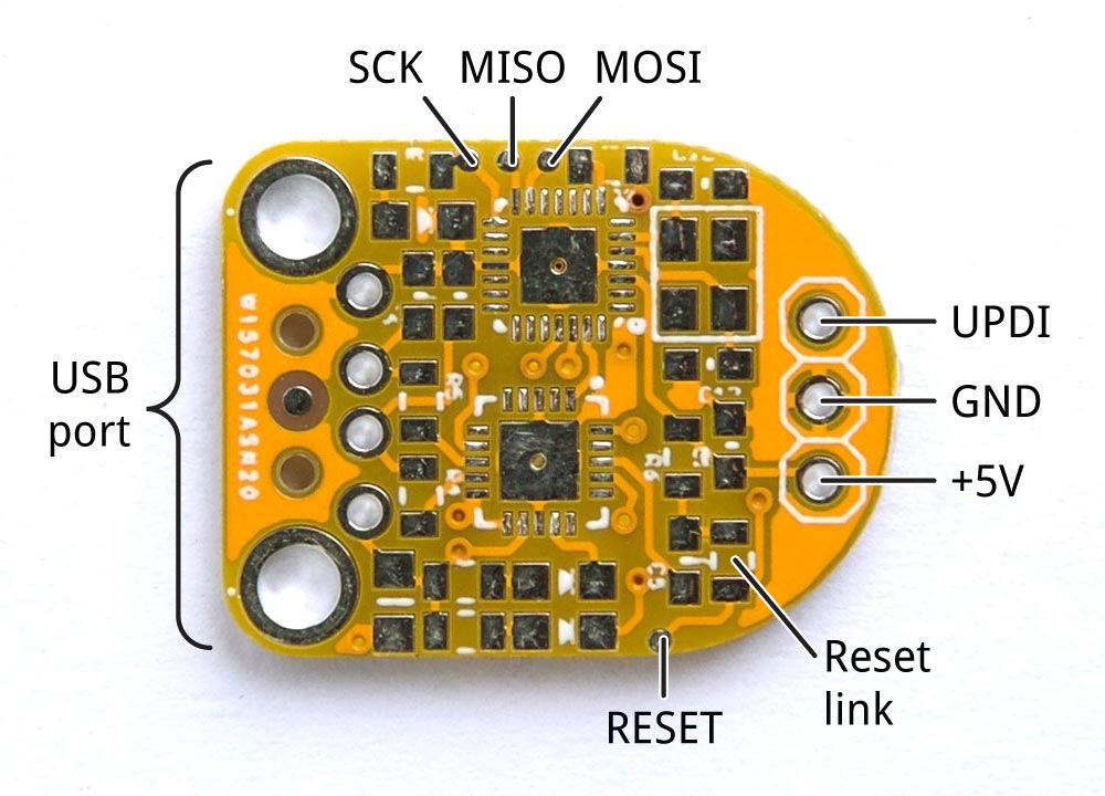
1. Solder a wire link in the position of the 0Ω resistor on the board. This connects the reset line to the microcontroller.
2. Solder wires to the MOSI, MISO, SCK, and RESET pads on the board, and connect these to header sockets that you can connect leads to. I recommend using very fine wires for the connections, so you don’t inadvertently lift the pads off the PCB. The other option is to solder header pins directly to the board.
3. Connect a 3-pin header to the three terminals at the top of the UPDI programmer PCB so you can use this to connect GND and 5V to the board.
4. Connect an ISP programmer to the board via the six wires you have provided. Do note that this could be an Arduino board like the UNO.
5. In the Arduino IDE choose Arduino/Genuino Uno from the Arduino AVR Boards section on the Boards menu, and set the Programmer to ArduinoISP if using the Arduino UNO or to the corresponding programmer name if using any other programmer.
6. Select the Port to which the Programmer is connected and Choose Burn Bootloader to upload the bootloader to the board.
Test the bootloader
With this successfully finished, you should now have the bootloader installed on the UPDI Programmer. You can test the success of the bootloader flashing process by uploading the Arduino Blink example to the UPDI Programmer via the USB port. Launch the example by going to File -> Examples -> Basic -> Blink. Select the board type, along with the port to which the board is connected. Hit the upload button and if all is well the red LED should flash on the UPDI Programmer Stick. If this fails, make sure you’ve uploaded a bootloader as described in the previous steps.
With the bootloader tested, the next task is to upload the jtag2updi code to the board.
Upload the UPDI Programmer Sketch(jtag2updi)
Follow the steps below to upload the jtag2updi programmer sketch to the UPDI Programmer stick.
Extract the zip file and open the jtag2updi folder.
Open the jtag2updi.ino sketch with the Arduino IDE, connect the UPDI Programmer stick to your computer via USB and upload the code just like you did for the blink sketch above.
Remove the wire you fitted earlier in the 0Ω resistor position on the UPDI Programmer board
That’s it, the board is now ready to be used as a UPDI Programmer but we have one more step to take. The UPDI is a protocol that is not part of the list of the programmer protocols that were shipped with the Arduino IDE. As such, for the Arduino IDE to recognize the board as a programmer, the megaTinyCore needs to be installed in the IDE. Steps to installing the megaTinyCore have already been covered in our last tutorial, in which we examined how you can turn an Arduino nano into a UPDI Programmer. You can follow those steps to install the megaTinyCore on the Arduino IDE.
Programming the Chips with the UPDI Programmer
The UPDI Programmer stick is ready and the Arduino IDE is ready for UPDI Programming. Follow the steps below to program your ATtiny-0-series microcontroller.
1. Connect the ATtiny to the UPDI Programmer stick as shown in the image below:
The connection is quite straightforward but the pin-pin connection between the Programmer and the Attiny is illustrated below to prevent mistakes:
2. With the microcontroller connected to your Arduino UPDI programmer, we are now ready to upload code to the ATtiny.
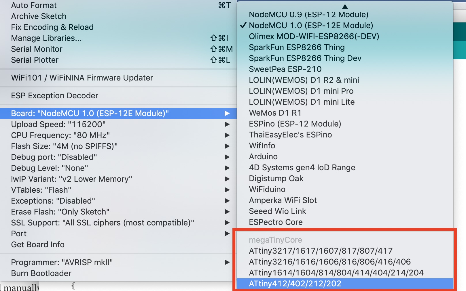
3. Open or write the code you would like to upload. Verify the code to ensure that there is no error, then go to Tools -> Board, and scroll down till you see the ATtiny you are working with on the list and select it. The ATtiny boards will be automatically installed after you install the megaTinyCore.
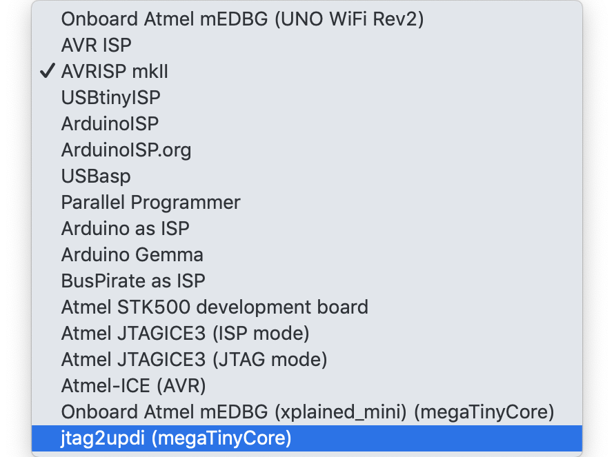
4. This should update the parameters being displayed when you click tools. Now we need to tell the Arduino IDE to use our programmer. To do this, go to Tools->Programmers (towards the end). Scroll down on the pane and select jtag2updi (megaTinycore) as your programmer.
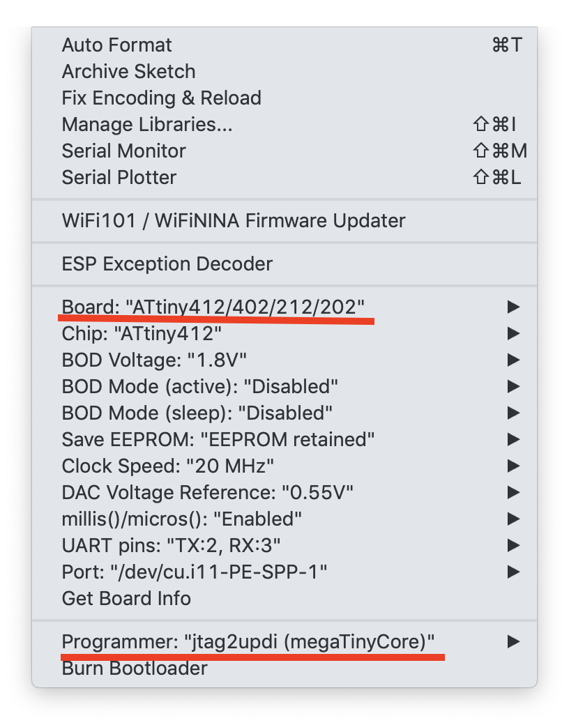
5. With that done, your screen should now look like the image below when you click on tools;
6. This means all lights are green. Now select the port to which the Programmer Stick is connected and hit the upload button on the IDE. You should immediately see the upload process and when complete, the microcontroller should perform as programmed.
There you go! Compared to the former ATtiny microcontrollers, these new series of MCUs come with higher amount of flash memories, cost a whole lot less and are all-around more efficient compared to the previous set as such they should probably be considered when next you are making the choice of a tiny low-cost, low-power microcontroller for your project and thanks to today’s project, you have a permanent programmer to sort their needs.
The capabilities of sensors and sensing systems have grown considerably in recent years, making data acquisition (DAQ) systems increasingly complex as the amount of data flowing and the processing required in these systems multiplies. FPGA devices are perfectly suited to high performance DAQ because of their flexibility, configurability, performance, and parallel processing capabilities. Data ingress and pre-processing with FPGAs is unmatched with any other technology.
From custom machine vision cameras to extremely sophisticated research-grade metrology and cutting-edge LIDAR systems, Opal Kelly modules and the FrontPanel SDK allow our customers to focus on their core competency to leap ahead of the competition and stay on the bleeding edge. Engineers leverage FrontPanel, relying on a proven system for professional-grade USB connectivity.
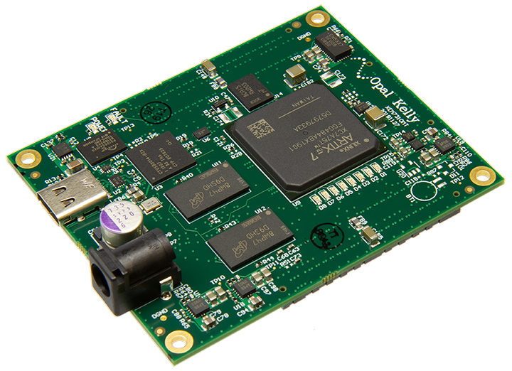
The XEM7310MT Artix-7 based FPGA module offers a turnkey SuperSpeed USB 3.0 host interface using Opal Kelly’s FrontPanel SDK. System designers can build fully-operational prototype and production designs quickly by integrating this device into their product. From multi-sensor aggregators to high-speed JESD-204B data acquisition and software-defined radio, the XEM7310MT provides multiple interfaces to manage data ingress and egress with the flexible and efficient power of FPGA processing to offload host processors.
Visit opalkelly.com to see our full line of FPGA modules for data acquisition and other FPGA applications.
XEM7310MT Product Features:
Xilinx Artix-7 XC7A75T or XC7A200T
SuperSpeed USB 3.0 interface (Cypress FX3) for configuration and data transfer
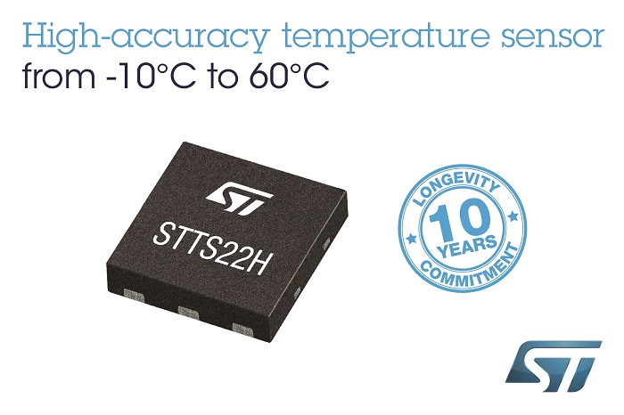
The STTS22H temperature sensor from STMicroelectronics offers high accuracy with low operating and standby current and flexible operating modes. By Gina Roos @ electronicproducts.com
STMicroelectronics has launched its STTS22H temperature sensor with typical temperature-reading accuracy of 0.25°C and low operating and standby current. The device enhances temperature and heat-flow monitoring in asset trackers, shipping-container loggers, HVAC systems, air humidifiers, refrigerators, building-automation systems, and smart consumer devices.
The STTS22H is I2C and SMBus 3.0 compliant, and supports flexible operating modes including configurable output data rate (ODR) down to 1 Hz, a power-saving one-shot mode, and an interrupt pin that supports SMBus alert response address (ARA). This allows the sensor, as an SMBus slave, to signal the application if a user-programmed upper or lower temperature threshold is exceeded, said STMicroelectronics. Programmable I²C/SMBus slave addresses allow up to two STTS22H sensors to share the same bus.
The device offers very low power consumption. It draws only 2.0 µA at 1 Hz ODR and 1.75 µA during periodic one-shot measurements, which extends the runtime of battery-powered devices. In standby mode with the serial port inactive, the STTS22H draws only 0.5 µA (typical). In addition, the 1.5-V to 3.6-V operating-voltage range allows use with various power sources such as a small lithium cell.
The fast-acting sensor offers a conversion time of 5 ms, and provides 16-bit temperature data. Devices come factory-calibrated and maintain the 0.25°C typical accuracy over the temperature range of -10°C to 60°C, eliminating any need for user calibration, according to the company.
The STTS22H, packaged in a 2.0 x 2.0 x 0.5 6-lead UDFN, is priced at $0.49 for orders of 1000 units.
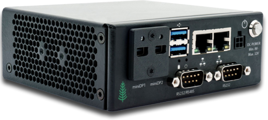
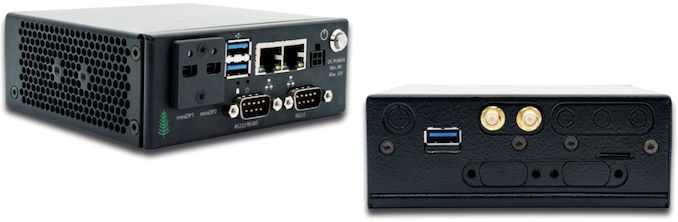
Simply NUC, the company behind several Intel NUC based SBCs like the Apollo Lake based NUC 8 Rugged, recently announced the launch of a new mini-computers codenamed; “Sequoia”.
The Sequoia
The Sequoia is Simply NUC’s first AMD-powered mini computer and it is aimed at applications around AI, Edge Analytics, robotics, POS, digital signage and industrial IoT or computing, thanks to it’s rugged and robust build.
The Sequoia is built around AMD® Ryzen™ processors, which gives it the ability to run most of the popular operating systems including; Windows 10 and several Linux distros, giving developers the flexibility to develop the exact solution they require without compromises.
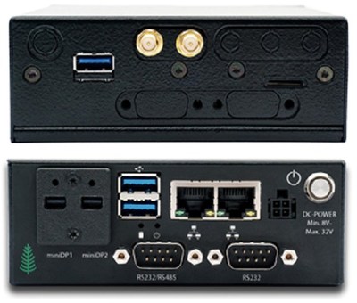
In terms of features, in order to accommodate the requirements for the plethora of applications for which the Sequoia can serve, and keep the Simply NUC’s tradition of providing all their Mini PCs with very extensive connectivity features, the Sequoia comes with two serial ports, two gigabit Ethernet ports (controlled using Intel’s i210-LM), two locking Mini Display Ports, Serial RS-232/Serial RS-485 video outputs, Wi-Fi 5 and Bluetooth 5, optional microSD card reader, and several USB 3.1 Gen 2 port. To give users additional connectivity options, the Mini PC also comes with three(3) M.2 slots through which things like a wireless-AC card, an LTE Modem and (or), an SSD storage device can be connected to the sequoia. To provide multiple mounting options, the chassis of the mini PC is designed to support DIN rail and VESA mounting plate, giving users a choice on how the device is installed.
The Sequoia was designed for reliable and long-lasting use in rugged environments, typical of industrial settings. It supports an automotive-grade power supply range (8 to 32Vdc) with a locking connector and is able to withstand a maximum relative humidity of 95% @ 40C and a wide operational temperature range of 0 to 60C. To enhance maintenance, the Sequoia also features a built-in health monitoring system which includes; a controllable fan, hardware monitoring and a watchdog timer.
To give users some level of options, Simply NUC two versions of the Sequoia exist; The Sequoia V8 and the Sequoia V6.
Simply NUC – Sequioa Mini Computer
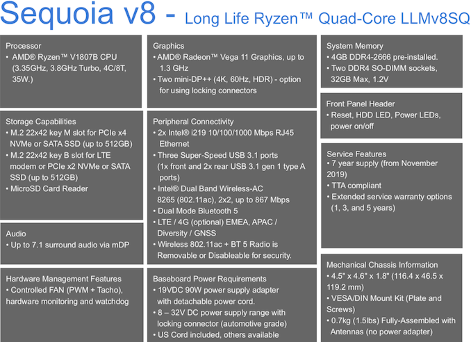
The Sequoia V8, also called the LLMv8SQ, is based on the AMD Ryzen V1807B Quad-Core Processor with 3.8GHZ turbo speed. It runs an AMD Radeon VEGA 11 graphic card at up to 1.3GHz speed. A breakdown of the features of the V8 is provided in the image below.
Sequoia V8
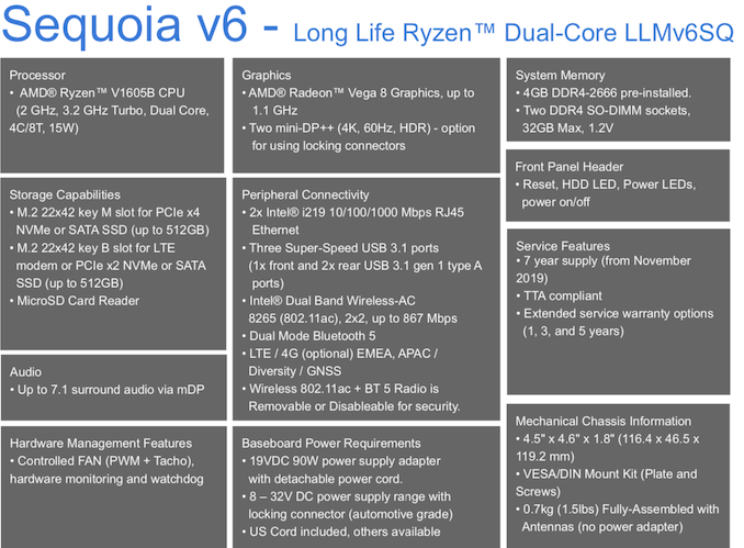
The Sequoia V6, on the other hand, is based on the AMD Ryzen V1605B Dual Core processor with 2GHz and 3.2GHz turbo speed. The Sequoia V6 runs the AMD Radeon VEGA 8 Graphics card. Some of the features of the V6 are highlighted in the image below.
Sequoia V6
Comparing the features, it is clear that the most important difference between these two models is the difference in the type of processor and graphics card used. This may be significant when you have to select between the two versions, especially if the use case is one with computational complexities.
According to Simply NUC’s product page for each of the MiniComputers, when ordering with default configurations, the Sequoia v6 will cost $689 while the Sequoia V8 will cost as much as $849 however, the product page allows users to select different add-ons and modification which could take the cost of each of the models way beyond these estimates.
Simply NUC’s is promising users a 7 years of support for the boards which is a huge relief, as one of the biggest challenges users have is manufacturers terminating support for a project just a year after developing it.
Boardcon‘s new EM-IMX8M-MINI is based on NXP’s energy-efficient i.MX8M Mini ARM Cortex A53 processor. The iMX8M SBC has 2GB LPDDR4 and 8GB of eMMC flash with 2x USB 2.0, GbE. Display output is via MIPI LCD, PCIe. There is also optional support for SSD/4G. It runs Linux 4.14.98 and QT 5.0.
EM-IMX8M-MINI SBC and its SOM-IMX8M-MINI module is Boardcon’s first i.MX8 family of boards. NXP’s i.MX8M Mini SOC, which is built into the separately available SODIMM-style SOM-IMX8M-MINI module that powers the new EM-IMX8M-MINI SBC. This SOC has appeared on various compute modules, many of which like Ibase’s recent RM-N8MMI SMARC module, are available with a carrier board.
Although the SOM-IMX8M-MINI module is available with any of the 1.8GHz Cortex-A53 i.MX8M Mini models, the EM-IMX8M-MINI board is only available with the quad-core model at this moment. The Mini SoC stocks a 400MHz Cortex-M4 MCU as well as GCNanoUltra and Vivante GC320 graphics processors.
SOM-IMX8M-MINI module
The 67.6 x 34.3mm SOM-IMX8M-MINI module comes with 2GB LPDDR4, 8GB eMMC. And for wireless connectivity is has the module 802.11b/g/n and Bluetooth 4.0. The 5V module has a PMIC and it runs Linux 4.14.98 with Qt 5.10.
And for EM-IMX8M-MINI board(118.6 x 102.3mm), it has a MicroSD slot along with MIPI-DSI and CSI connectors, and analog and digital audio interfaces, including a Wolfson codec. There are 2x USB host ports, single micro-USB OTG port, single Nano-SIM, Ethernet, and UART RS-232 ports. There are also other I/O options like UART, I2C, RS485, CAN, GPIO, SPI, and JTAG. An M.2 slot supports an optional 4G module or SSD.
EM-IMX8M-MINI detailed view
Specification Summary of the Boardcon EM-IMX8M-MINI:-
Processor: NXP i.MX8M Mini Quad (4x Cortex-A53 @ up to 1.8GHz);
GPU: GCNanoUltra for 3D, GC320 for 2D GPUs; Cortex-M4F @ 400MHz
Memory: 2GB LPDDR4 RAM; 8GB eMMC 5.1; QSPI NOR flash
Networking/wireless:
10/100/1000 Ethernet port (Realtek RTL8211E)
802.11n and Bluetooth 4.0 (via SOM-IMX8M-MINI and Ampak AP6236 modules)
4G available on M.2 slot
Media I/O Options:
MIPI-DSI (4-lane) for up to 1920 x 1080p 60fps
MIPI-CSI (4-lane)
3.5mm audio jack
Speaker header
Wolfson WM8960 audio codec
5x SAI digital audio interfaces (8-bit RX and TX)
Other I/O:
2x USB 2.0 host ports
Micro-USB OTG port
RS-232 DB9 port
3x UARTs
RS-485
CAN
26-pin header with 2x I2C, 6x GPIO, SPI
JTAG debug; separate debug for Cortex-M4
Expansion: M.2 E-key (PCIe 2.1) slot for 4G or SSD; nano-SIM slot, MicroSD slot
Power: 5V/3A DC input jack; ROHM BD71847 PMIC; power, power key, and reset switches
Operating System: Linux 4.14.98 BSP with Qt 5.0
Further information
The EM-IMX8M-MINI SBC and SOM-IMX8M-MINI module are available now on the product pages of Boardcon’s EM-IMX8M-MINI and SOM-IMX8M-MINI.
The startup Print2Taste has kept its promise also in its second Kickstarter campaign. Several backers already received their 3D Choco printer. According to Print2Taste the project team did a great job – the shipment started even ahead of schedule.
mycusini is the first consumer 3D Choco printer which came up successfully on Kickstarter.
In terms of production quality and speed there is no difference to professional 3D food printers for 2.000 € and more. It is now regularly available at www.mycusini.com for 298 € only. Print2Taste guarantees delivery before Christmas.
The mycusini is reduced to the max, with only 19 x 19,5 x 27 cm it is smaller than most coffee machines and fits into every kitchen. It is powered by special 3D Choco refills provided by Print2Taste – success guaranteed.
Easy-to-make Choco text messages, more than 200 creative objects already on board and easy operation will ensure a maximum fun factor.
With its much higher printing speed than plastic, mycusini also brings benefits to schools and educational institutions.