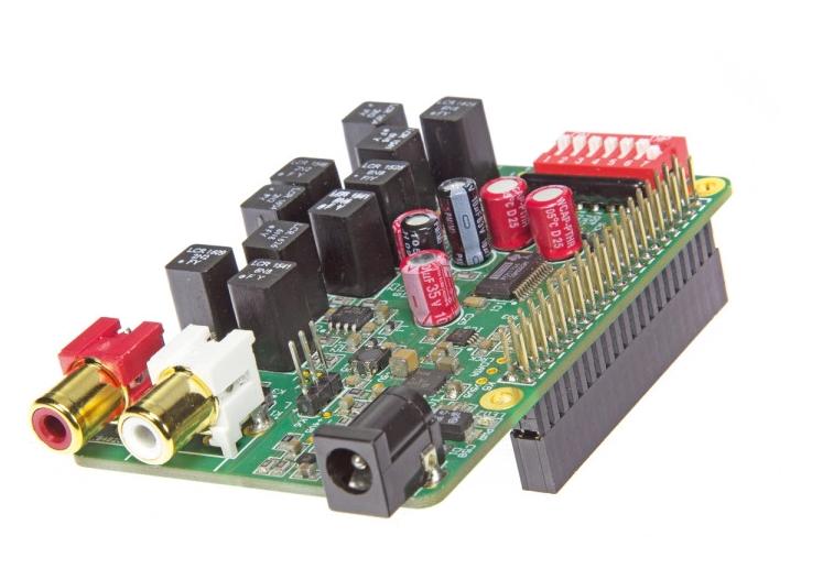
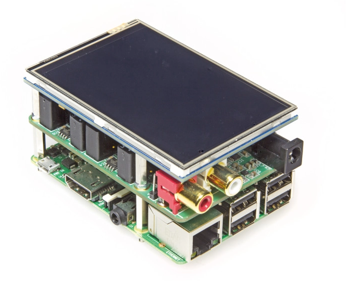
Small single-board computers like the Raspberry Pi are ideal for use as small stand-alone network audio players. With Volumio and other specialized Linux distributions, putting together an audio player is remarkably easy. And as Elektor staff member Ton Giesberts shows in the referred article, you can also use this approach to build a high-end audio player.
Note: Since its publication of the project in 2017, components, software elements, webpages and other elements mentioned in the article may be subject to updating to the present day.
Original publication: Elektor magazine 5/2017.
Author: Ton Giesberts (Elektor Labs).
Free download expires: Friday 1 November, 2019.
Go to the article page and download a pdf copy of the magazine article. Downloading is free until Friday 1 November, 2019.
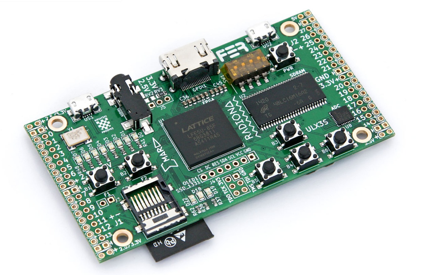
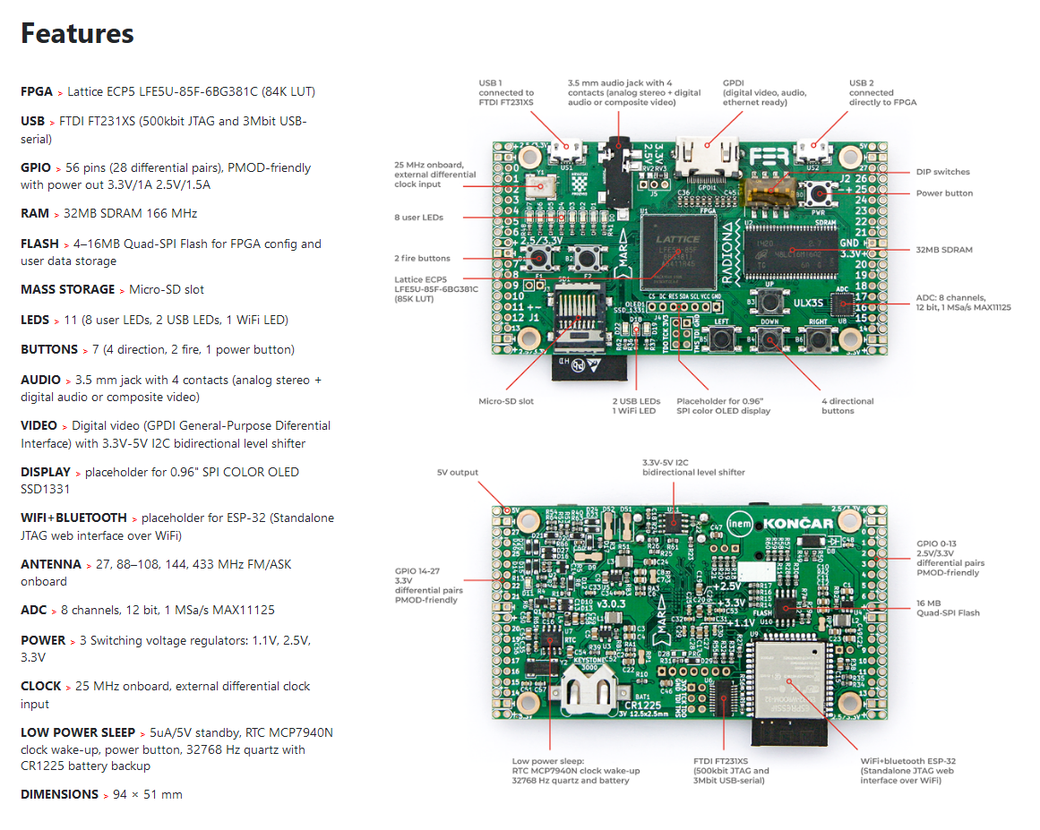
ULX3S is a fully open source, compact, robust, and affordable FPGA dev board equipped with a balanced selection of additional components and expansions. Although it was designed primarily as a teaching tool for mastering the principles of digital circuit design, ULX3S incorporates a wide array of features and interfaces that allow it to serve as a broadly useful module for installation in complex devices.
Built around a powerful Lattice Semiconductor ECP5-series FPGA chip and supported by the latest open-source toolchains, ULX3S is one of the most powerful and desirable platforms available for FPGA enthusiasts. It comes equipped with onboard Wi-Fi, display, buttons, LEDs, and storage. Flash it with an over-the-air (OTA) update using the Wi-Fi connection or take advantage of the onboard OLED display and buttons to browse the contents of an SD card and select a bitstream. Due to its battery-backed RTC, ULX3S can power down completely and wake up only in response to certain events. This feature makes it perfect for use in low-power applications such as battery-powered remote sensor nodes.
And if you’re not the low-power type, onboard peripherals like SDRAM, USB, digital video out, onboard FM/ASK antenna, ADC, and DAC make it an audio/video powerhouse for signal processing and synthesis, motor control, and SDR use cases. It can emulate arcade machines and retro computers like the Minimig (Amiga) or modern systems like the F32C (MIPS/RISCV). It has 56 GPIO pins, all routed as differential pairs, and a PMOD compatible pinout, which opens it up to a wide range of expansion options. And if you are just starting out FPGAs, you can use the Arduino IDE to program ULX3S in seconds.
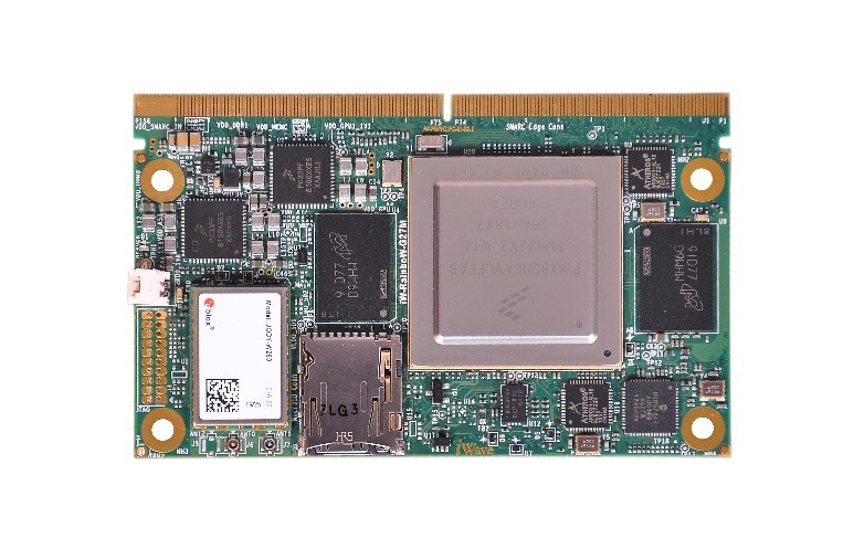
iWave systems recently launched a new SMARC System on Module (SOM) based on the powerful NXP® i.MX 8QuadMax applications processors. This high performance SOM features an intelligent blend of MPUs+MCU power in a single device and integrates heterogeneous multicore 64 bit ARM® processors (Dual Cortex® A72@ 1.8 GHz + Quad Cortex® A53 @ 1.2 GHz and Dual Cortex® -M4F @ 266 MHz), targeted for applications that demand advanced real-time processing, multi-media performance as well as in applications that requires simultaneous multi-OS operations.
The Cortex® M4F microcontroller plays an integral part in realizing various real-time operations of the SOM module. It is a powerful energy-efficient microcontroller core with floating-point arithmetic functionality that offers a low-latency execution environment with real-time and low-power processing capability running bare-metal code or a real-time operating system like FreeRTOS.
The Cortex® ‑M4F microcontroller incorporates the following key features:
A processor core.
A Nested Vectored Interrupt Controllerfor low-latency interrupt processing.
Multiple high-performance bus interfaces.
Memory Protection Unit(MPU) & Floating Point Unit (FPU).
LPIT (Low-power Periodic Interrupt Timer) for periodic timer services
TPM (Timer PWM Module) for timer and PWM services
RGPIO (Rapid General-Purpose Input/Output) for the fast pin I/O capability
MU (Messaging Unit) for interprocessor communication
INT MUX (Interrupt Mux) to select local interrupts routed outside of the subsystem
SEMA42 (hardware semaphore) for HMP synchronization to shared resources
LPI2C (Low-Power I2C) for serial communication
LPUART (Low-Power UART) for serial communication and debug
Optimized performance and efficiency for real-time processing:
To optimize performance and increase system efficiency it is always effective to separate computation tasks between various Cortex® cores. The Cortex® A cores runs high-level OS
(Linux /Android) and can be used to drive applications that demand compute-intensive graphics (2D/3D), 4K video, high speed data processing etc., while real-time applications such as sensor monitoring, data acquisition, motor control, etc., requires high degree of determinism and DSP capability which can be handled very efficiently by the RTOS running on the Cortex® M4F cores. In addition, the SOM supports simultaneous operation of multiple OS platforms that enables the cores to drive totally independent applications, for e.g. When the Cortex® A cores handle a system for HMI or an instrument cluster, the Cortex® M4F can drive the circuitry for sensor control while utilizing RPC for interprocessor communications.
High-speed data acquisition:
On applications that make use of high-speed RF synthesis (ADC conversion), the Cortex® -M4F core can be employed to acquire analog inputs at a high sample rate and offload the Cortex® A cores for instantaneous processing of the acquired data. For instance, in the case of industrial automation, where devices are often deployed in remote locations, the Cortex® -M4F core continuously monitors various sensor operations and can instantly detect any signal variations and communicates it with Cortex® A cores for instantaneous processing of the acquired data.
Intelligent power management:
In applications where the Cortex® A cores waits for communication from the Cortex® M4F cores, the system can take control of the situation and power gate the Cortex® A cores. The Cortex® A cores can go to sleep mode and can be activated either using predefined wake-up time or when there is a user-defined interrupt generated by Cortex® M4F core. While the Cortex® A core is shut down, the Cortex® M4F continues to monitor the system in low power, thereby optimizing the power intakes.
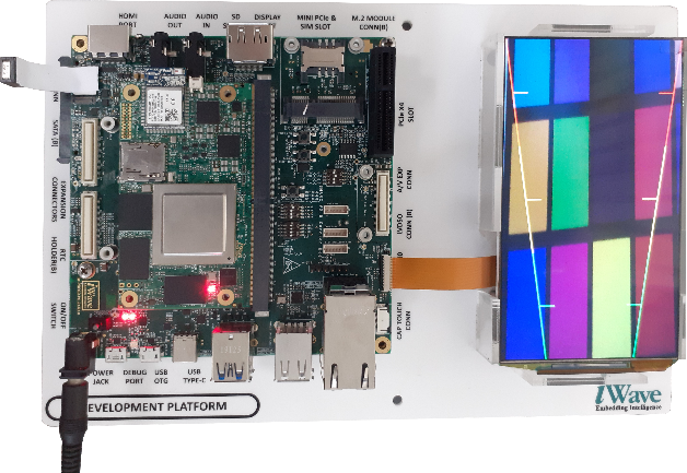
Rear-view camera application using the Cortex®M4F of i.MX8QM SMARC SOM
iWave Systems have validated the real-time performance of i.MX8QM SOM by demonstrating an application for the rear-view camera using only the Cortex® M4F of the SOM. The application demonstrates the fast boot capability of the Cortex® M4F which is interfaced with the camera sensors mounted at the rear of the vehicle. After powering on the board in just 3 secs camera application starts to run. Cortex® M4F acquires data from the camera sensors and displays the image/video on the rear-view mirror thereby aiding the users to reverse park their vehicles with ease.
Likewise, several industrial applications ranging from Automation, Drones, HMI, and High-End signage, both real-time and non-real time can be easily enabled using iWave’s powerful i.MX8QM SMARC SOM platform.
With 10+ years longevity, custom SOM configuration and dedicated technical support including carrier board review, software support, etc., designers and OEMs can be assured of iWave’s unwavering quality and long-term service. Our support resources include detailed hardware and software user manual, carrier board schematics, BSP package with toolchain support, reference designs, etc.,
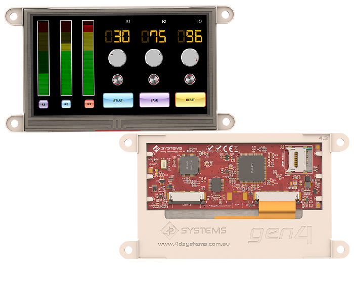
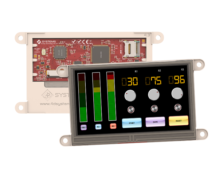
The gen4 4.3” Diablo16 Integrated Display Modules are part of the latest gen4 series of modules Designed and Manufactured by 4D Systems.
The gen4 series was designed specifically for ease of integration and use, with careful consideration for space requirements and functionality.
These specific gen4 modules feature a 4.3” colour TFT LCD display, and come with options for Cover Lens Bezel (CLB), Resistive Touch and Capacitive Touch. They is powered by the well-known 4D Systems Diablo16 Graphics Processor, which offers an array of functionality and options for any Designer / Integrator / User.
The 4.3” Diablo16 Integrated Display Module features a TFT LCD Display, is capable of Touch Detection, microSD memory Storage, GPIO and Communications, along with multiple millisecond resolution timers, and Audio Generation.
The gen4 Series is 100% compatible with the Workshop4 IDE and its 4 different development environments, providing the user with a wealth of options for programming and controlling their system.
The gen4 series of Integrated Display Modules feature a 30 pin ZIF socket, designed for a 30 pin FFC cable, for easy and simple connection to an application or mother board, or for connecting to accessory boards for a range of functionality advancements.
The gen4 series of modules have been designed to minimise the impact of display related circuitry, and provide a platform suitable for integration into a product. Application boards can sit flush on the back of the gen4 display module if required, as the display related electronics sit inside the plastic mounting base, leaving the application board surface clear for User circuitry.
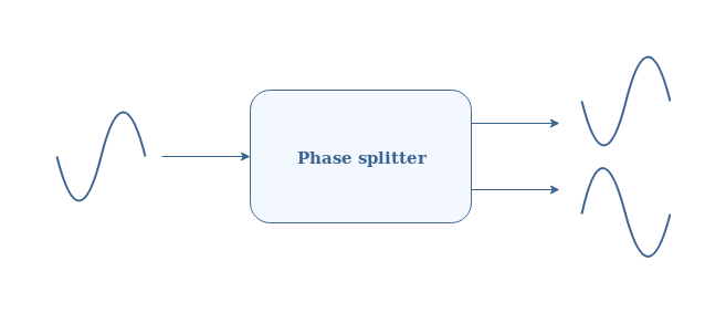
Often, not only the amplitude of the signal is interesting to transform, such as amplifiers do, but also its phase. Bipolar transistors can indeed be used in the design of a device called a phase splitter.
fig 1 : Flow chart of a phase splitter
In the very first section, general notions about the phase and the properties of a phase splitter are given, so we understand the context. The second section will present the architecture of a phase inverter based on the design of a common emitter and common collector amplifiers.
Not only BJT transistors can be used to make phase splitters, but we will see in a third section that a more interesting phase splitter can be designed with operational amplifiers (OA). Moreover, we detail a particular case of OA-based phase splitter in a next section that can be used to make a phase modulator.
General concepts and presentation of the phase splitter
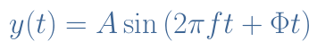
Any periodic signal has three important parameters that fully define it : the amplitude A, the frequency f and the phase Φ. A sinusoidal signal y(t) can for example be written such as shown in Equation 1 :
eq 1 : Formula of a sine signal
The value of the phase dictates the value of y(t=0). Actually, the value of the phase of a signal is not important and does not have any impact on the signal itself. As an example, if you listen to an audio signal, you will never distinguish the difference between a 0° or 90° phase signal.
Moreover, without having access to initial conditions or a reference, it can not be measured : the same thing happens with the electric potentials. However, such as for electric potentials, a phase shift or phase difference can be measured between two signals and this value is useful.
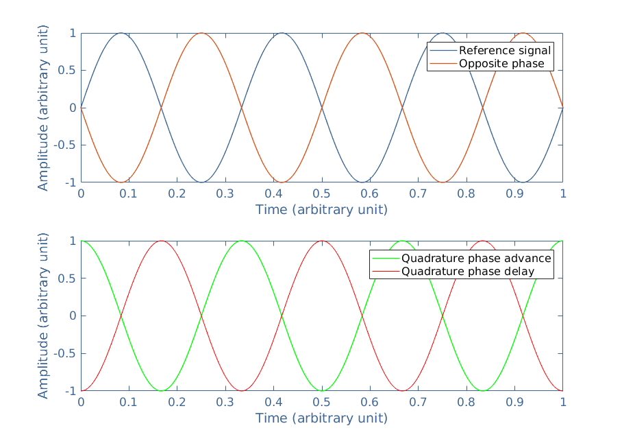
Let’s consider two sine signals that have the same frequency but different phases Φ1 and Φ2. The phase shift φ is a constant value and it is simply defined by φ=Φ1-Φ2. If we consider a reference signal of phase Φr=0°, three notable phase shifts can be highlighted as shown in Figure 1 :
fig 2 : Definition of phase opposition and quadrature. Plotted with MatLab®
An opposition phase is shifted of 180° or π rad with respect to the reference signal. Quadrature phases are shifted of +90° or +π/2 rad for the phase advance and –90° or -π/2 rad for the phase delay.
Most of the time, the goal of phase splitters is to generate two outputs : one reference and an opposition or quadrature phase shifted signal. During this operation, no amplification of the signal is necessary and phase splitters usually have a unit gain to only modify the phase.
BJT-based phase splitter
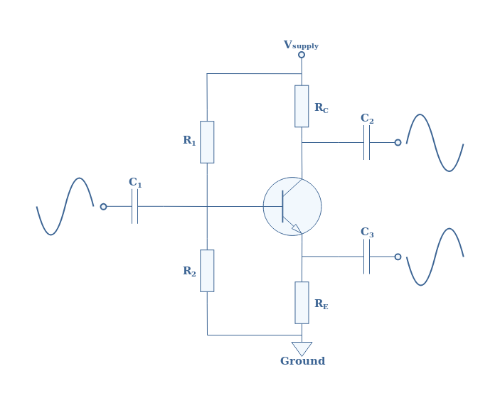
A phase inverter, that is to say a phase splitter that shifts the signals of 180° can be built with combining a common emitter and a common collector amplifiers. The architecture of the BJT-based phase splitter is shown in the Figure 3 :
fig 3 : BJT-based phase splitter
We recognize in this figure the emitter-follower structure wired to the emitter branch and the common emitter structure wired to the collector branch. Let’s analyze separately how these two architecture works, the reader should not hesitate to refer to the Common Emitter and Common Collector (emitter-follower) tutorials for the following.
Concerning the common emitter part of this design (RC and C2), the voltage gain is equal to -RC/RE. By setting RC=RE, the voltage gain becomes -1 so that the first output signal conserve the same amplitude as the input but with its phase inverted. This signal is commonly known as the inverting output.
For the emitter-follow part (RE and C3), the voltage gain is intrinsically equal to +1. The output is therefore conserving the same amplitude and phase as the input. This signal is known as the non-inverting output.
Operational amplifier-based phase splitter
A phase splitter can also be designed with an operational amplifier (OA) and a potentiometer. The advantage of this configuration is that, unlike the BJT-based phase splitter where the phase is only inverted, it can here vary from 0° to almost 360°.
We distinguish two setups for an OA-based phase splitter : the delay and advance phase splitters. In Figure 4 below, the architecture of a delay phase splitter is presented :
fig 4 : Delay OA-based phase splitter
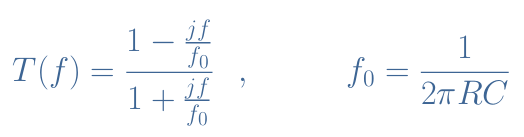
By applying Millman’s theorem, we can show that the transfer function T(f) of this circuit is given by the following formula :
eq 2 : Transfer function of the delay phase splitter
The delay phase splitter respects that the gain of the signal is equal to 1. Indeed we can note that the numerator of T(f) is a complex number and its denominator is the conjugate complex of the numerator. Since the module of the complex conjugate is equal to the module of the same complex number, the module of T(f) is equal to 1.
Moreover, the evolution of the phase Φ(f) with the frequency is given by Arg(T(f)) which is the argument of the transfer function. It can be shown that Φ(f,RP)=-2Arctan(2πRPCf), the phase is therefore directly influenced by the value of the potentiometer RP. We can note that in the case of the delay phase splitter, the phase shift is negative and for a potentiometer that can vary such as shown in Figure 4, the value is between -160° and 0°.
Positive phase shifts can be accessed with an advance phase splitter, its architecture shown in Figure 5 is slightly different :
fig 5 : Advance OA-based phase splitter
In this case, the phase shift is expressed just as for the delay phase splitter but with an opposite sign : Φ(f,RP)=+2Arctan(2πRPCf).
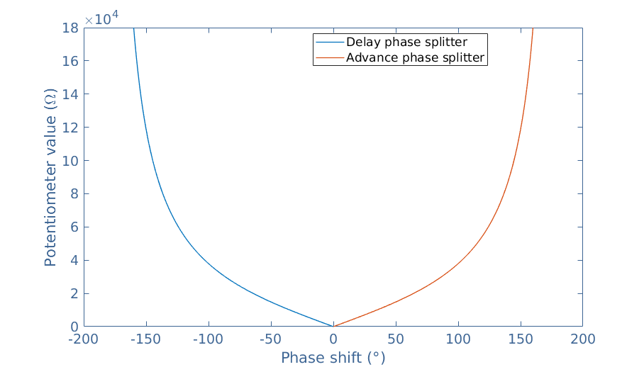
When combining the circuits of Figure 4 and 5 in cascade (in serie), a large range of phase shifts can be accessed as shown in the following graph :
fig 6 : Possible phase shift for a delay and advance phase splitter cascade. Plotted with MatLab®
Phase modulator
Having understood how an OA-based phase splitter works, we can now design a very useful device called a phase modulator performing phase modulation (PM). A PM consists of transforming the phase of a carrier signal in order to be able to transmit information.
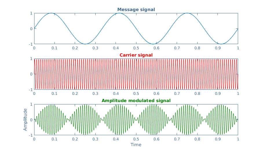
The most visual modulation technique is the amplitude modulation (AM) and represented in Figure 7. It consists in multiplying the message signal (low frequency) with a carrier signal (high frequency fc). The message is contained in the envelope of the modulated signal and can be recovered by using low-pass filters.
fig 7 : Amplitude modulation technique. Plotted with MatLab®
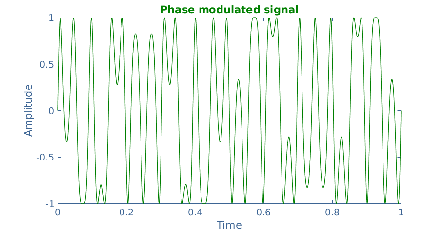
In PM technique, instead of modulating the amplitude, we modulate the phase. Unlike for the AM technique, it is not very visual and easy to estimate how the original message signal looks like by only observing the phase modulated signal :
fig 8 : Phase modulated signal. Plotted with MatLab®
A phase modulator can be built by modifying the OA-based phase splitter. The capacitor is replaced by a field effect transistor (MOSFET) which gate is controlled by the carrier signal such as shown in Figure 9.
fig 9 : Architecture of a phase modulator
Mathematically, originally the message signal is of the form such as shown in Equation 1. The phase modulator circuit of Figure 9 transforms the signal such as the phase modulated signal pm(t) contains a function phase Φ(t) instead of a constant phase and is of the form presented in Equation 3 :
eq 3 : Expression of the phase modulated signal
Conclusion
Phase transformation is another great function that BJT and OA-based amplifiers can perform. Phase shifting has many applications among which phase modulation and balanced topology drivers (driving push-pull configurations for example) are the most known.
In the first section of this tutorial, we have clearly defined what are the phase and the phase shift. This last one is an important property that gives the temporal spacing between two signals. A phase shift can be from -180° to +180° which represents the point where the two signal are in opposition. The -90° and +90° values are called quadrature shifts and it is important to know how to shift two signals from such values since some important applications (wireless LAN for example) use this property.
The first circuit we have presented, is capable of performing phase splitting, and is a combination of common emitter and common collector amplifiers. We have seen that this configuration can provide two outputs : one identical to the input and one phase inverted signal. It is a simple design and the phase shift is constant and cannot be modified by an external command.
In the next section, we have presented an operational amplifier (OA) based phase splitter that can overcome the constant phase shift problem of the BJT-based phase splitter. We have indeed seen that depending on the position of the capacitor in the circuit, an advance or delay phase splitter can be made by combining the use of a variable resistance. This circuit enables to obtain a the full range of phase shifting possible between -180° and +180° if the variable resistance can reach a high enough value.
Finally, in the last section we have proposed a modified version of the OA-based phase splitter in order to design a phase modulator. This architecture includes a MOSFET connected to the non-inverting terminal of the OA that is controlled by a carrier signal. This phase modulator performs a phase modulation which is one of the techniques along with the amplitude (AM) and frequency modulation (FM) that are used in telecommunications.
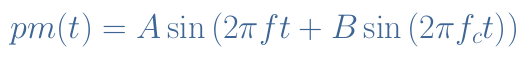
OriginGPS has announced its first dual-frequency GNSS module, the ORG4600-B01, which will enable customers to build systems with sub-1m accuracy without implementing external components. by Jean-Pierre Joosting @ www.mwee.com
Measuring just 10- x 10-mm, the ORG4600-B01 module supports L1 + L5 GNSS reception with one RF port, enabling the use of a low-cost, dual-band antenna delivering sub-1m accuracy performance in real-world operating conditions. An alternate build option allows for separate L1/L5 RF outputs when dual antennas are required. The module is ideally suited for systems requiring ultra-accurate positioning, such as telematics, IoT and OBD applications.
OriginGPS collaborated with Broadcom to create a new miniature module with L1 + L5 support provided by the BCM47758 chip, enabling ultra-accurate GNSS positioning. The module was developed for solutions requiring super-precision GNSS and a dual frequency combination.
“This year has seen several satellites launched into orbit every month, most of them fitted with L5/E5 capabilities, and the Chinese and European Union governments plan to have their satellite constellations fully operational by 2020. Developing the ORG4600-B01 module with the BCM47758 GNSS receiver chip by Broadcom was the fastest and surest way to add a high quality dual frequency module to our portfolio and meet our customers’ increasing requirements for ultra-accurate GNSS modules,” said Haim Goldberger, CEO of OriginGPS.
“Size is a crucial parameter in GNSS dual frequency solutions,” said Prasan Pai, product marketing director for the Wireless Communications and Connectivity Division at Broadcom. “The collaboration with OriginGPS has created the industry’s smallest dual-frequency module with ‘no compromise’ quality. The collaboration enables Broadcom to reach new markets, such as precision agriculture, security, children tracking and fleet management.”
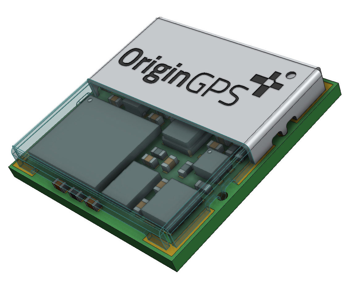
Kontron, a leading global provider of IoT/Embedded Computing Technology (ECT), introduces motherboards “Designed by Fujitsu” including the form factors (Thin) Mini-ITX, µATX, Mini-STX, and ATX based on the latest Intel® platforms. As a result of the acquisition of Fujitsu’s products, production facilities and engineering in Augsburg, Germany, Kontron has expanded its embedded motherboard product portfolio.
The new Kontron motherboards are based on the Intel® Coffee-Lake platform and, with an extensive BIOS update, enable the use of the new 9th generation Intel® processors based on the proven Fujitsu design. This gives customers who are already using the boards the advantage of deploying the latest processors directly and without any hardware replacements. The refresh with the first eight-core processor in the LGA1151 socket means an increase in performance through an optimization of the processor technology and allows up to 5GHz clock frequency in the top model with Intel® Core™ i9-9900K processor. For Kontron, the new motherboards are part of the first new product introductions from the Fujitsu product range previously taken over. Kontron continues to develop, produce and certify the boards in Germany, from where technical support is also provided.
The current industrial motherboards “Designed by Fujitsu” support processors up to 98W. The Mini-ITX motherboards D3633-S and D3634-S are equipped with a chipset of the Intel®-300 series and offer extensive graphic interfaces such as DVI-D, DP, LVDS and eDP despite their small form factor. The D3641-S µATX and the D3646-S ATX, on the other hand, feature an extremely powerful Intel® C246 chipset including Intel® iAMT and Intel® Xeon™ support. All motherboards offer a variety of interfaces such as SATA, USB 3.1 and various COM ports.
The latest extended lifecycle motherboards are especially designed for semi-industrial applications. The portfolio includes the formats Mini-STX, Thin Mini-ITX, µATX as well as various interfaces state of the art connectivity such as Display Port, HDMI and USB 3.1.
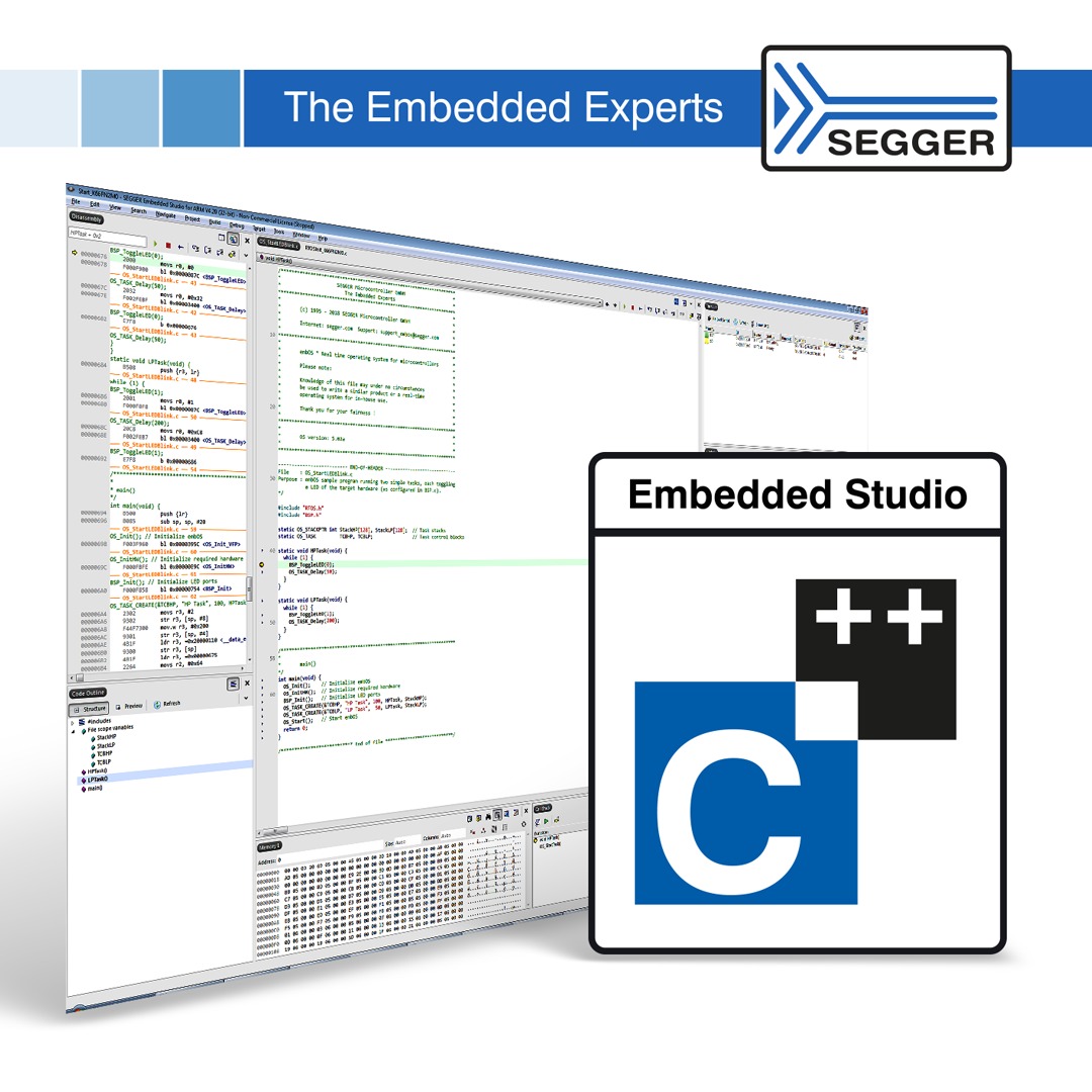
The latest release of Embedded Studio, SEGGER’s cross-platform IDE, can now debug software on evaluation boards equipped with a DAP-Link (CMSIS-DAP) debug interface. This new feature is included in the ARM and Cortex-M editions on all supported host platforms: Windows and Linux 64- and 32-bit, as well as macOS (including Catalina). The software to access the DAP-Link is based on the proven J-Link software. It can download directly into flash memory, and is optimized for both stability and performance.
While an on-board J-Link delivers superior features and performance, DAP-Link is used on a number of low-cost evaluation boards. Embedded Studio now makes using these boards easy. It simply works, out of the box, hassle-free. One download and install is all it takes.
“Knowing boards with DAP-Link are commonly used by hobbyists and students, we are excited to give them access to our professional IDE and software libraries,” says Johannes Lask, Product Manager for Embedded Studio at SEGGER. “This also enables SEGGER and others to create evaluation software projects for Embedded Studio and these boards, in line with our ‘It simply works!’ philosophy. I believe that Embedded Studio, due to its ease of use and easy licensing, is the best choice for silicon vendors to make reference projects and SDKs available.”
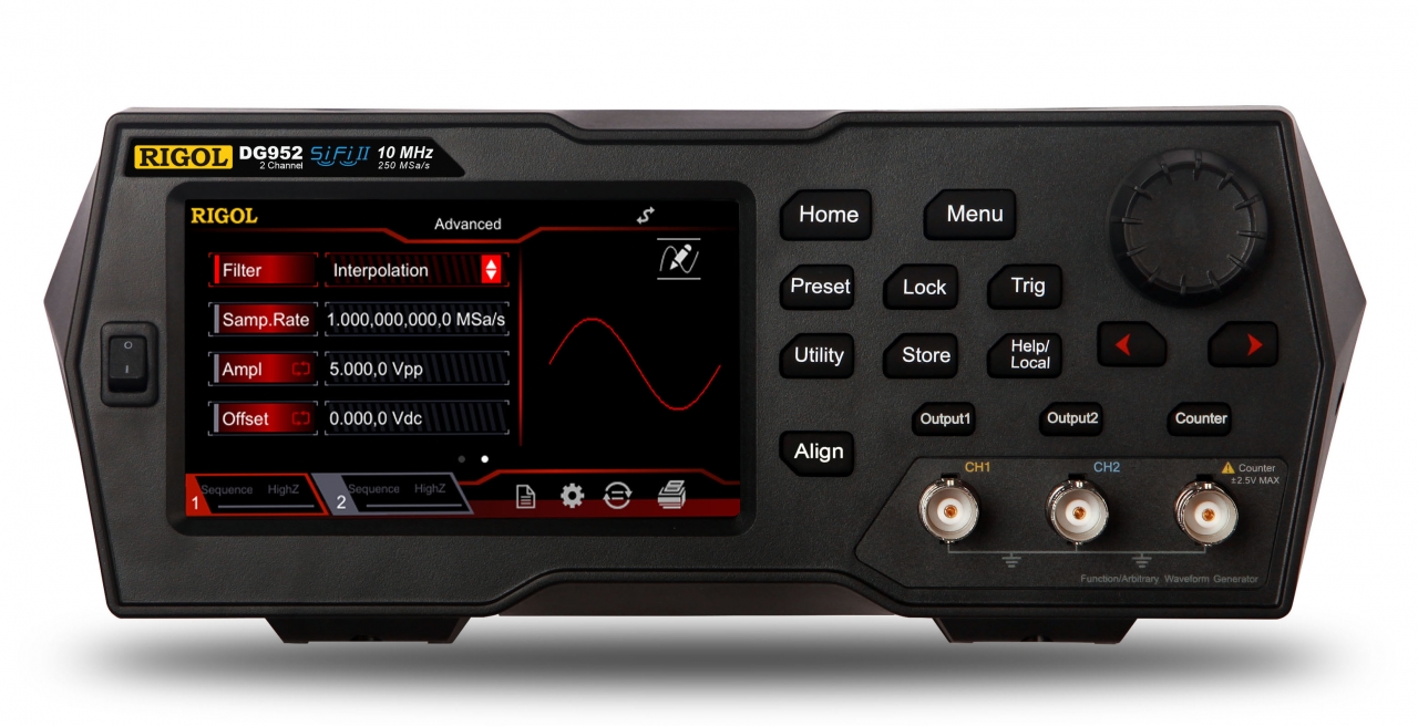
The Rigol DG952 50MHz Dual Channel Function Generator, although value-priced, provides highly-accurate 16-bit standard and arbitrary waveforms point by point from its huge 16Mpt memory. Most other AWGs are only 14-bit or less. With a sampling rate of 250MSa/sec, this versatile signal source produces precise, very low jitter waveforms (High frequency stability: ±1 ppm; low phase noise: -105 dBc/Hz). A 4.3” Touch Display provides exceptional control and waveform viewing. The Touch-enabled user-interface design provides a brand new operation experience, even supporting tap and drag operations. You can also use the keyboard to complete the parameter settings.
No cooling fan is required due to very clever ergonomic and functional case design, so audible noise is non-existent! The unit can output 1.0mVpp to 10Vpp into 50ohm to 10MHz, to 5Vpp at 25MHz, and up to +/- 2.5Vpp at 50MHz. Analog and digital modulation functions include: AM, FM, PM, ASK, FSK, PSK, and PWM. Arbitrary waveform sequence and waveforms also can be generated or edited through the available PC software. Also included is a built-in 7 digit 240MHz bandwidth full-featured frequency counter. Up to 160 built-in arbitrary waveforms cover the common signals in most engineering applications, medical electronics, auto electronics, math processing, and other fields.
Features:
Unique SiFi II (Signal Fidelity II) technology: generate the arbitrary waveforms point by point; recover the signal without distortion; sample rate accurate and adjustable; jitter of all the output waveforms (including Sine, Pulse, etc.) as low as 200 ps
6 Mpts memory depth per channel for arbitrary waveforms
Standard dual-channel with the same performance, equivalent to two independent signal sources
High frequency stability: ±1 ppm; low phase noise: -105 dBc/Hz
Built-in high-order harmonic generator (at most 8-order harmonics)
Built-in 7 digits/s, 240 MHz bandwidth full featured frequency counter
Up to 160 built-in arbitrary waveforms, covering the common signals in engineering application, medical electronics, auto electronics, math processing, and other various fields
Sample rate up to 250 MSa/s, vertical resolution 16 bits
Arbitrary waveform sequence editing function available; arbitrary waveforms also can be generated through the PC software
Various analog and digital modulation functions: AM, FM, PM, ASK, FSK, PSK, and PWM.
Standard waveform combine function, capable of outputting specified waveforms combined with the basic waveforms
Standard channel tracking function, when enabled, all the parameters of both channels are updated based on users’ configurations
USB Host&Device interface (standard); USB-GPIB function supported
4.3” TFT color touch screen
RS232, PRBS, and Dualtone outputs supported
The DG952 is an excellent, versatile 16-bit dual-channel 50MHz signal generator with a performance and feature set normally reserved for much more expensive instruments.
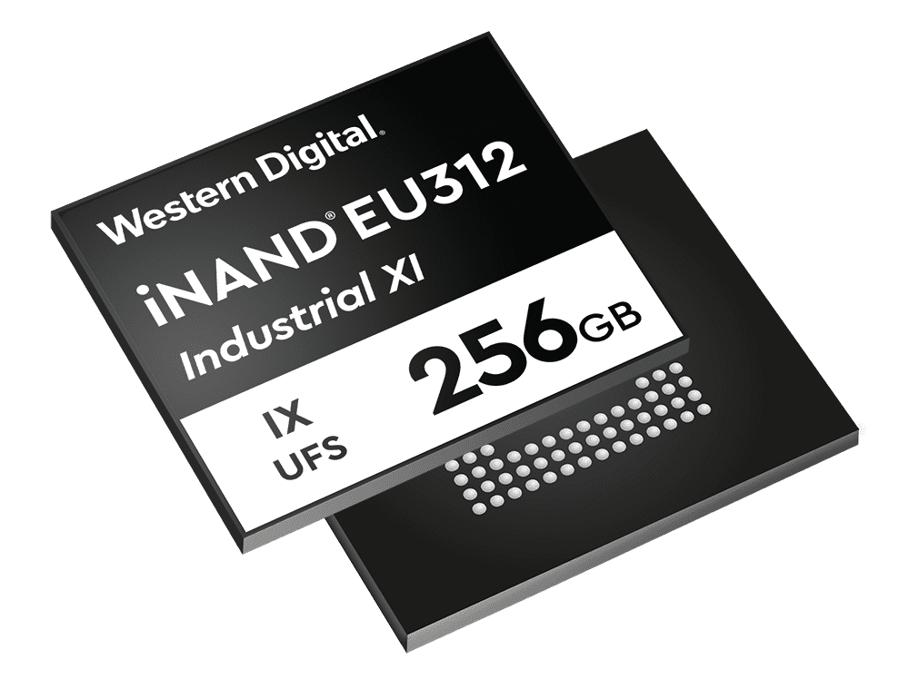
iNand IX EM132 – Industrial Embedded Flash Device.
The Industrial iNAND IX EM132 Embedded Flash Drive (EFD) is Western Digital’s most advanced e.MMC flash storage solution for industrial applications, with high reliability and endurance across a wide range of operational requirements.
Designed and tested to withstand demanding environmental conditions, this industrial- grade flash device features advanced flash memory management firmware to provide enhanced power immunity, ECC, wear leveling, and bad block management. Data intensive applications can rely on the EM132 to capture every critical moment, log each event, and to ensure quality-of-service to end-users.
The Smart Partitioning feature in the iNAND IX EM132 EFD Industrial flash devices allows Boot partitions, RPMB, multiple General-Purpose Partitions, User Data Area and Enhanced User Data Area, providing OEMs the flexibility to choose different attributes on a single device depending on storage requirements.
In addition, the optimized 3D NAND memory offers significant advantages over that of standard X2 MLC memory in the previous eMMC generation.
Product Highlights
Operating Temp Range: –40°C to 85°C on Industrial Extended Temperature SKUs; –25°C to 85°Con Commercial and Industrial SKUs
Broad portfolio: 8GB to 64GB
Extended product life cycle for industrial grade
Advanced controller built for endurance and reliability
High endurance: up to 3K P/E cycles in MLC
Smart Partitioning, Advanced Health Report and Manual Refresh (Industrial Grade)